Table of Contents
Advertisement
Quick Links
Advertisement
Table of Contents

Subscribe to Our Youtube Channel
Related Manuals for Prestigio T200C


Summary of Contents for Prestigio T200C
- Page 3 Preface TabletNote Computer T200C/T210C T200V/T210V Service Manual...
- Page 4 Preface Notice The company reserves the right to revise this publication or to change its contents without notice. Information contained herein is for reference only and does not constitute a commitment on the part of the manufacturer or any subsequent ven- dor.
-
Page 5: About This Manual
Preface About this Manual This manual is intended for service personnel who have completed sufficient training to undertake the maintenance and inspection of personal computers. It is organized to allow you to look up basic information for servicing and/or upgrading components of the computer. The following information is included: Chapter 1, Introduction, provides general information about the location of system elements and their specifications. -
Page 6: Related Documents
Preface Related Documents You may also need to consult the following manual for additional information: User’s Manual on CD This describes the computer’s features and the procedures for operating the computer and its ROM-based setup program. It also describes the installation and operation of the utility programs provided with the computer. -
Page 7: Table Of Contents
Model Differences ................1-2 Bottom (T200C) ................A-3 System Specifications T200C/T210C ..........1-3 14.1" LCD (T200C) ............... A-4 System Specifications T200D/T210D ..........1-5 Hard Disk Drive (T200C) .............. A-5 System Specifications T200V/T210V ..........1-7 Top (T210C) .................. A-6 System Specifications T200H/T210H ..........1-9 Bottom (T210C) ................A-7 External Locator - Top View with LCD Open ......1-11... - Page 8 Preface Clock Generator ................B-11 LVDS Transmitter, Panel I/F ............C-10 ICH4-1 ..................B-12 Clock (W311 + W256) ..............C-11 ICH4-2 ..................B-13 VT2835 (1 of 3) ................C-12 ICH4-3, HDD ................B-14 VT2835 (2 of 3) ................C-13 USB2.0 Port ................. B-15 VT2835 (3 of 3) ................
-
Page 9: Introduction
1: Introduction Overview This manual covers the information you need to service or upgrade the T200C/T210C/T200D/T210D/T200V/T210V/ T200H/T210H TabletNote computer. Information about operating the computer (e.g. getting started, and the Setup util- ity) is in the User’s Manual. Information about drivers (e.g. VGA & audio) is also found in User’s Manual. That manual is shipped with the computer. -
Page 10: Model Differences
Introduction Model Differences The differences between the model types are indicated in the table and pictures below. Specifications Table 1 - 1 T200C T200D T200V T200H Feature/Model Model T210C T210D T210V T210H Specifications Processor Type Intel Pentium® M Intel Pentium® M... -
Page 11: System Specifications T200C/T210C
Winkey Keyboard 4 Hardware Buttons: Pointing Device & Built-In TouchPad “Q” for screen rotation/power Buttons Escape Scroll Up/Scroll Down/Enter Indicators 7 LED Indicators (Power/Suspend, Battery, HDD, Caps Lock, Scroll Lock, Num Lock, Wireless LAN) System Specifications T200C/T210C 1 - 3... - Page 12 Standard - 1800mAH x 6 cells (40W) Optional - 1800mAH x 8 cells (53W) CD-ROM DVD-ROM Handwriting Recognition Utility CD-RW Car Adapter Combo MDC Module (factory option) DVD-RW Intel Pro 2100 (802.11b) Mini PCI Wireless LAN Module DVD+RW 1 - 4 System Specifications T200C/T210C...
-
Page 13: System Specifications T200D/T210D
Introduction System Specifications T200D/T210D Table 1 - 3 T200D/T210D Feature Specification T200D & T210D System µ Processor Types Intel Pentium® M Processor (478-pin) Micro-FCPGA 0.13) 0.13 Micron Process Technology, 1MB On-Die L2 Specifications Package Cache & 400MHz Front Side Bus - 1.3/ 1.4/ 1.5/ 1.6/ 1.7 Core Logic Intel®... - Page 14 Introduction Feature Specification T200D & T210D Interface & Two USB 2.0/1.1 Ports One RJ-45 Jack for 100M (Max) Fast Ethernet Communication One Type-II PCMCIA 3.3V/5V Socket Intel Pro 2100 (802.11b) Mini PCI Wireless LAN Module One Stereo Headphone-Out Jack One External (VGA) Monitor Port One Monaural Microphone-In Jack One DC-in Jack One RJ-11 (V.90 K56flex™) Jack for Fax/Modem...
-
Page 15: System Specifications T200V/T210V
Introduction System Specifications T200V/T210V Table 1 - 4 T200V/T210V Feature Specification T200V & T210V System Processor Types VIA Antaur 1.0 GHz Specifications Core Logic CLE266CE Security Security (Kensington® Type) Lock Slot BIOS Password Memory Two 200 Pin DDR SODIMM Sockets Supporting 256/512MB DDR RAM Modules Supporting DDR 266 MHz Modules Expandable up to 1024 MB... - Page 16 Introduction Feature Specification T200V & T210V Power Supports ACPI v1.0b Supports Resume From Modem Ring Management Supports Hibernate Mode Supports Resume From LAN Supports Standby Mode Close Cover Switch Supports Battery Low Sleep Power Full Range AC adapter One Primary Smart Lithium-Ion (1800mAH x 6 cells) AC Input 100~240V, 50~60Hz Battery Pack with Gas Gauge DC Output 20V, 2.5A, 50W...
-
Page 17: System Specifications T200H/T210H
Introduction System Specifications T200H/T210H Table 1 - 5 T200H/T210H Feature Specification T200H & T210H System Processor Types VIA Antaur 1.0 GHz Specifications Core Logic CLE266CE Security Security (Kensington® Type) Lock Slot BIOS Password Memory Two 200 Pin DDR SODIMM Sockets Supporting 256/512MB DDR RAM Modules Supporting DDR 266 MHz Modules Expandable up to 1024 MB... - Page 18 Introduction Feature Specification T200H & T210H Power Supports ACPI v1.0b Supports Resume From Modem Ring Management Supports Hibernate Mode Supports Resume From LAN Supports Standby Mode Close Cover Switch Supports Battery Low Sleep Power Full Range AC adapter One Primary Smart Lithium-Ion (1800mAH x 6 cells) AC Input 100~240V, 50~60Hz Battery Pack with Gas Gauge DC Output 20V, 2.5A, 50W...
-
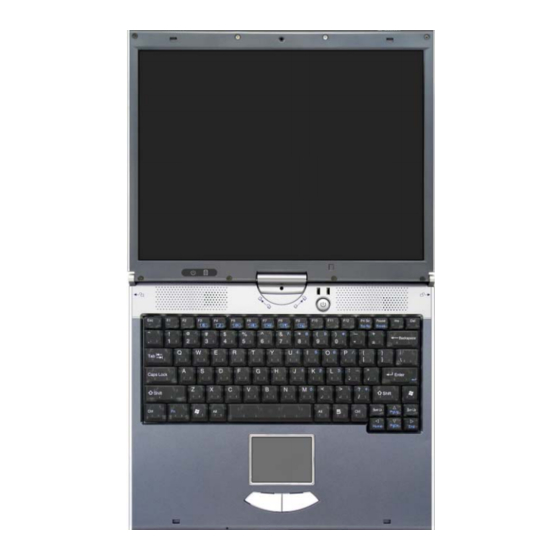
Page 19: External Locator - Top View With Lcd Open
External Locator - Top View with LCD Open Figure 1 - 2 Top View with LCD Panel Open Built-In PC Camera (Optional) LCD Swivel Screen LED Power Indicators Cover Sensors T200C/T200V T210C/T210V LCD Swivel Hinge T200D/T200H T210D/T210H LCD Side Hinges Power Button Speakers Keyboard 10. TouchPad and Buttons 11. -
Page 20: Rotating The Lcd Swivel Screen
Introduction Rotating the LCD Swivel Screen Figure 1 - 3 Rotating the LCD Swivel Screen Lid Button recommended that the lid (left LCD cover sensor) power button to should be set to “Do nothing” in the Power Options control panel. This will prevent acci- dentally triggering a power saving mode... - Page 21 Introduction Touch Panel Warning Touch Panel Input Device Users should be very careful not to press too hard with the stylus pen when using it as the input device. Only the approved stylus pen provided should be used as the input device. Users should avoid sliding the stylus pen (or any object) in the area around the edge of the Do not use any sharp screen (between the LCD and the frame) when writing on the screen, or pointed objects as...
-
Page 22: External Location - Front & Rear Views
Introduction External Location - Front & Rear Views Figure 1 - 5 Front View LCD Latches Microphone-In Jack Headphone-Out Jack Infrared Transceiver Scroll/Enter Wheel LED Status Indicators 3 * Hot-Key Buttons (Esc, Tab, & “Q” Rotate) Figure 1 - 6 Rear View 8. -
Page 23: External Locator - Left & Right Views
Introduction External Locator - Left & Right Views Figure 1 - 7 Left View Security Lock Slot Vent Stylus Pen Holder Figure 1 - 8 Right View 4. 4-in-1 Flash Card Reader 2 * USB 2.0 Ports PC Card Slot External Locator - Left &... -
Page 24: External Locator - Bottom View
Introduction External Locator - Bottom View Figure 1 - 9 Bottom View Stylus Pen Holder Battery Intel WLAN Module Cover Modem & Wireless LAN Module Cover Hard Disk Cover T20XC/T2X0D Series RAM Cover CPU Cover Fan Intake Wireless Device Operation Aboard Aircraft The use of any porta- ble electronic trans-... -
Page 25: T2X0C/T2X0D Mainboard Overview - Top
Introduction T2X0C/T2X0D Mainboard Overview - Top Figure 1 - 10 T2X0C/T2X0D Key Parts Mainboard Overview - Top Key Parts 1. Intel ICH4 421 2. CardBus ENE CB710 3. LAN Controller RTL8100BL 4. Hitachi H8 5. NS 87393 6. Clock Generator T2X0C/T2X0D Mainboard Overview - Top 1 - 17... -
Page 26: T2X0C/T2X0D Mainboard Overview - Bottom
Introduction T2X0C/T2X0D Mainboard Overview - Bottom Figure 1 - 11 T2X0C/T2X0D Key Parts Mainboard Overview - Bottom Key Parts 1. CPU Socket (no CPU installed) 2. Memory Sockets 3. WLAN Module Socket 4. PCMCIA Socket 5. Intel 855GM(E) 732 Micro FCBGA 6. -
Page 27: T2X0C/T2X0D Mainboard Overview - Top
Introduction T2X0C/T2X0D Mainboard Overview - Top Figure 1 - 12 T2X0C/T2X0D Cable Connectors Mainboard Top Cable Connectors 1. Speakers (CN4/ CN5) 2. Keyboard (CN10) 3. Buttons (CN12) 4. Microphone (CN13) 5. LED Board (CN3) 6. Inverter (CN6) 7. LCD (CN9) T2X0C/T2X0D Mainboard Overview - Top 1 - 19... -
Page 28: T2X0C/T2X0D Mainboard Overview - Bottom
Introduction T2X0C/T2X0D Mainboard Overview - Bottom Figure 1 - 13 T2X0C/T2X0D Cable Connectors Mainboard Bottom Cable Connectors 1. Hard Disk (CN25) 2. CMOS Battery (CN31) 3. Hot_Key Board(CN27) 4. CPU Fan (CN18) 5. Battery (CN24) 1 - 20 T2X0C/T2X0D Mainboard Overview - Bottom... -
Page 29: T2X0V/T2X0H Mainboard Overview - Top
Introduction T2X0V/T2X0H Mainboard Overview - Top Figure 1 - 14 T2X0V/T2X0H Key Parts Mainboard Overview - Top Key Parts 1. South Bridge VT-8235 2. Super I/O VT1211 3. PCMCIA ENE CB710/BGA 4. LAN/PHY VT6103 5. Micro-P H8/2140 6. LVDS VT1631 Transmitter, Panel I/F T2X0V/T2X0H Mainboard Overview - Top 1 - 21... -
Page 30: T2X0V/T2X0H Mainboard Overview - Bottom
Introduction T2X0V/T2X0H Mainboard Overview - Bottom Figure 1 - 15 T2X0V/T2X0H Key Parts Mainboard Overview - Bottom Key Parts 1. VIA-C3 Processor (surface mounted) 2. Memory Sockets 3. PCMCIA Module Slot 4. North Bridge VT-8623 5. Flash ROM BIOS 6. 4-in-1 Card Reader Module Socket 7. -
Page 31: T2X0V/T2X0H Mainboard Overview - Top
Introduction T2X0V/T2X0H Mainboard Overview - Top Figure 1 - 16 T2X0V/T2X0H Cable Connectors Mainboard Top Cable Connectors 1. Speakers (CN4/ CN5) 2. Inverter Board (CN3) 3. LED Board (CN6) 4. Keyboard (CN10) 5. LCD (CN9) 6. TouchPad(CN12) 7. Microphone (CN13) T2X0V/T2X0H Mainboard Overview - Top 1 - 23... -
Page 32: T2X0V/T2X0H Mainboard Overview - Bottom
Introduction T2X0V/T2X0H Mainboard Overview - Bottom Figure 1 - 17 T2X0V/T2X0H Cable Connectors Mainboard Bottom Cable Connectors 1. Hot-Key Board (CN27) 2. Wireless LAN(CN26) 3. Modem (CN23) 4. CMOS Battery(CN31) 5. Hard Disk (CN25) 6. Battery (CN24) 7. CPU Fan (CN18) 8. -
Page 33: Disassembly
The model types differ very slightly in appearance (when viewed from the bottom), however the disassembly pro- cedures are identical with the exception of the Wireless LAN and modem modules. The pictures used throughout the disassembly procedures are of the T200C model. Overview 2 - 1... -
Page 34: Maintenance Tools
Disassembly NOTE: All disassembly procedures assume that the system is turned OFF, and disconnected from any power supply, and that all peripheral cables are disconnected (including telephone lines and network cables). Maintenance Tools The following tools are recommended when working on the computer: •... -
Page 35: Maintenance Precautions
Disassembly Maintenance Precautions The following precautions are a reminder. To avoid personal injury or damage to the computer while performing a re- moval and/or replacement job, take the following precautions: Power Safety Warning 1. Don't drop it. Perform your repairs and/or upgrades on a stable surface. If the computer falls, the case and other components could be damaged. -
Page 36: Disassembly Steps
Disassembly Disassembly Steps The following lists the disassembly steps, and on which page to find the related information. PLEASE PERFORM THE DISASSEMBLY STEPS IN THE ORDER INDICATED. To remove the battery: 1. Remove the battery page 2 - 5 To remove the hard disk drive: 1. -
Page 37: Removing The Battery
Disassembly Removing the Battery Figure 2 - 1 Battery Removal 1. Turn the computer off, and turn it over. Sequence 2. Locate the battery bay as highlighted in Figure 2 - 3. Slide the battery lock in the direction of the arrow a. -
Page 38: Removing The Hard Disk
Disassembly Removing the Hard Disk Figure 2 - 2 Hard Disk Removal 1. Turn the computer off, and turn it over and remove the battery (page 2 - Sequence 2. Remove screw from the hard disk cover. 3. Slide the hard disk assembly in the direction of the arrow a. -
Page 39: Removing The System Memory (Ram)
Disassembly Removing the System Memory (RAM) Figure 2 - 3 RAM Removal 1. Turn the computer off, and remove the battery (page 2 - Sequence 2. Remove screws from the memory socket cover , and remove the cover. 3. Gently pull the two release latches on the sides of the memory socket in the direction of the arrows ( &... -
Page 40: Removing The Intel Wlan Module (T2X0C/T2X0D Only)
Disassembly Removing the Intel WLAN Module (T2X0C/T2X0D Only) Figure 2 - 4 T2X0C/T2X0D Intel 1. Turn the computer off, and remove the battery (page 2 - WLAN Module 2. Remove screw from the WLAN module cover, and remove the cover Removal Sequence 3. -
Page 41: Removing The Processor (T2X0C/T2X0D Only)
Disassembly Removing the Processor (T2X0C/T2X0D Only) Figure 2 - 5 T2X0C/T2X0D You can only upgrade the T2X0C/T2X0D model’s processor (the T2X0V/T2X0H model’s processor is surface mounted Processor Removal and cannot be removed). Sequence 1. Turn the computer off, and remove the battery (page 2 - 2. - Page 42 Disassembly 2 - 10...
-
Page 43: Part Lists
Over the product life, some parts may be improved or re-configured, resulting in new part numbers. Part List Illustration Location The following table indicates where to find the appropriate part list illustration. Table A- 1 Part T200C T210C T200V T210V Part Lists... -
Page 44: Top (T200C
Part Lists Top (T200C) Figure A-1 (T200C) 鋁箔 A - 2 Top (T200C) -
Page 45: Bottom (T200C
Part Lists Bottom (T200C) Figure A - 2 Bottom (T200C) Bottom (T200C) A - 3... -
Page 46: Lcd (T200C
Part Lists 14.1" LCD (T200C) Figure A - 3 14.1" LCD (T200C) A - 4 14.1" LCD (T200C) -
Page 47: Hard Disk Drive (T200C
Part Lists Hard Disk Drive (T200C) Figure A-4 Hard Disk Drive (T200C) Hard Disk Drive (T200C) A - 5... -
Page 48: Top (T210C
Part Lists Top (T210C) Figure A-5 (T210C) 鋁箔 A - 6 Top (T210C) -
Page 49: Bottom (T210C
Part Lists Bottom (T210C) Figure A-6 Bottom (T210C) Bottom (T210C) A - 7... -
Page 50: Lcd (T210C
Part Lists 14.1" LCD (T210C) Figure A-7 14.1" LCD (T210C) A - 8 14.1" LCD (T210C) -
Page 51: Hard Disk Drive (T210C
Part Lists Hard Disk Drive (T210C) Figure A-8 Hard Disk Drive (T210C) Hard Disk Drive (T210C) A - 9... -
Page 52: Top (T200V
Part Lists Top (T200V) Figure A-9 (T200V) 鋁箔 A - 10 Top (T200V) -
Page 53: Bottom (T200V
Part Lists Bottom (T200V) Figure A-10 Bottom (T200V) Bottom (T200V) A - 11... -
Page 54: Lcd (T200V
Part Lists 14.1" LCD (T200V) Figure A-11 14.1" LCD (T200V) A - 12... -
Page 55: Hard Disk Drive (T200V
Part Lists Hard Disk Drive (T200V) Figure A-12 Hard Disk Drive (T200V) Hard Disk Drive (T200V) A - 13... -
Page 56: Top (T210V
Part Lists Top (T210V) Figure A-13 (T210V) 鋁箔 A - 14 Top (T210V) -
Page 57: Bottom (T210V
Part Lists Bottom (T210V) Figure A-14 Bottom (T210V) Bottom (T210V) A - 15... -
Page 58: Lcd (T210V
Part Lists 14.1" LCD (T210V) Figure A-15 14.1" LCD (T210V) A - 16 14.1" LCD (T210V) -
Page 59: Hard Disk Drive (T210V
Part Lists Hard Disk Drive (T210V) Figure A-16 Hard Disk Drive (T210V) Hard Disk Drive (T210V) A - 17... - Page 60 Part Lists A - 18...
-
Page 61: T200C/T210C Schematic Diagrams
Schematic Diagrams Appendix B: T200C/T210C Schematic Diagrams This appendix has circuit diagrams of the T200C/T210C computers PCB’s: Table B - 1 Diagram - Page Diagram - Page Schematic Diagram System Block Diagram - Page B - 2 PCMCIA ENE CB710 - Page B - 18... -
Page 62: System Block Diagram
Schematic Diagrams System Block Diagram Sheet 1 of 30 System Block CLOCK GEN. ICS950810 Diagram CPU PSB_CLK(100MHz) Intel ADAPTER MCH PSB_CLK(100MHz) 100~240V AC/DC ITP PSB_CLK(100MHz) Pentium-M PCI LAN_CLK(33MHz) 128/256/512MB DDR SDRAM 1.3~1.8GHz PCI PCM_CLK(33MHz) V_CORE LPC SIO_CLK(33MHz) DDR SO-DIMM 1 +VCCP LPC H8_CLK(33MHz) +VDD3... -
Page 63: Pentium
Schematic Diagrams Pentium-M-1 Sheet 2 of 31 Pentium-M-1 H_REQ#[4:0] U40A H_D#[0:63] U40B H_D#[0:63] [5] H_D#0 H_D#32 A20M# H_A20M# [11] D32# H_REQ#0 H_FERR# H_D#1 AA24 H_D#33 REQ0# FERR# H_FERR# [11] D33# H_REQ#1 H_D#2 H_D#34 REQ1# IGNNE# H_IGNNE# [11] D34# H_REQ#2 H_D#3 H_D#35 REQ2# STPCLK#... -
Page 64: Pentium-M-2
Schematic Diagrams Pentium-M-2 Sheet 3 of 31 Pentium-M-2 +1.8VS_PROC 1.7GHz & 1.468V = 24.5W U40D V_CORE 1.6GHz & 1.468V = 24.5W VSS0 VSS96 R461 0_0805 +1.8VS VSS1 VSS97 1.5GHz & 1.468V = 24.5W VSS2 VSS98 +1.8VS FOR BANIAS CPU VSS3 VSS99 C541 C540... -
Page 65: 855Gm-1
Schematic Diagrams 855GM-1 Sheet 4 of 31 855GM-1 C817 *33P U39E C818 *33P M_DATA[63:0] M_DQS[8:0] [8] U39B M_DATA0 M_DQS0 C819 *33P SDQ0 SDQS0 Z0402 M_DATA1 M_DQS1 SDQ1 SDQS1 T129 DVOBD0 BLUE DAC_BLUE [9] M_DATA2 M_DQS2 Z0403 T127 SDQ2 SDQS2 DVOBD1 BLUE# M_DATA3 AE12... -
Page 66: 855Gm-2
Schematic Diagrams 855GM-2 Sheet 5 of 31 855GM-2 U39A H_A#[31:3] H_D#[63:0] [2] H_A#3 H_D#0 GMCH Strapping Options HA3# HD0# H_A#4 H_D#1 HA4# HD1# H_A#5 H_D#2 HA5# HD2# External Thermal Sensor Header H_A#6 H_D#3 HA6# HD3# H_A#7 H_D#4 HA7# HD4# H_A#8 H_D#5 FUNCTION Board Default... -
Page 67: 855Gm-3
Schematic Diagrams 855GM-3 Sheet 6 of 31 855GM-3 For 855GME, +1.2VS -> +1.35VS +1.2VS U39C C104 C533 VSS0 VSS84 AA16 U39D VSS1 VSS85 AE16 0.1U_X7R 0.1U_X7R 0.1U_X7R 0.1U_X7R 0.1U_X7R 150U/6.3V_D VSS2 VSS86 VCC0 VTTLF0 +VCCP 150U/6.3V_D VSS3 VSS87 VCC1 VTTLF1 C547 VSS4 VSS88... -
Page 68: Ddr Sodimm
Schematic Diagrams DDR SODIMM Sheet 7 of 31 DDR SODIMM M_DATA_R_[63:0] +2.5V M_DATA_R_[63:0] [8] +2.5V CN17 CN21 DDR_SO-DIMM1_R DDR_SO-DIMM2_S PCB Footprint = SODIMM-DDR_200P_R PCB Footprint = SODIMM-DDR_200P M_AA0 M_AA_FR_0 [4,8] M_AA0 M_AA_FR_0 [8] M_AB1 M_DATA_R_0 M_AA1 M_AB2 M_DATA_R_1 M_AA2 [4,8] M_AB[2:1] M_AA[2:1] [4,8] M_DATA_R_2... -
Page 69: Ddr Termination
Schematic Diagrams DDR Termination Sheet 8 of 31 +1.25VS DDR Termination +1.25VS +1.25VS C639 0.1U_X7R C339 0.1U_X7R M_CB_R3 RN23 8P4RX22 M_CB3 M_AA12 M_AA_FR_12 M_AA9 M_AA_FR_9 RN33 8P4RX56 RN10 8P4RX56 C635 0.1U_X7R C342 0.1U_X7R M_AA7 M_AA_FR_7 M_CB_R4 M_AA2 [4,7] M_AA2 M_DATA7 RN47 8P4RX22 M_DATA_R_7... -
Page 70: Lvds, Crt
Schematic Diagrams LVDS, CRT Sheet 9 of 31 LVDS, CRT +5VS +3VS R348 4.7K Z0906 +5VS R347 +5VS +5VS +5VS SCS751V 4.7K +5VS R645 4.7K DAC_DDCADATA [4] 2N7002 +3VS Z0920 C798 BAV99 BAV99 BAV99 SCS751V 0.1U R346 4.7K VGA DSUB Z0907 R345 +5VS... -
Page 71: Clock Generator
Schematic Diagrams Clock Generator Sheet 10 of 31 Clock Generator FREQUENCY SETUP TABLE (FS2) (FS1) (FS0) 3V66 66MHz OUT HCB2012K-121T30 VDD48 +3VS (MHz) (MHz) (MHz) (MHz) C351 C663 66.66 66.66 66.66 33.33 66.66 66.66 33.33 10U_0805 0.1U 66.66 66.66 33.33 66.66 66.66 33.33... -
Page 72: Ich4-1
Schematic Diagrams ICH4-1 Sheet 11 of 31 ICH4-1 +VCCRTC R188 R470 +3V_ALWAYS 100K U24A SMB_CLK R244 2.2K PCIRST# [15,16,17] PRST# ICH4-M PART A Z1104 SMB_DATA R472 2.2K [15,16,17] PCI_AD[31:0] SM_INTRUDER# PCI_AD0 BSS138 PCI_AD0 SMLINK0 PCI_AD1 System Manamement I/F PCI_AD1 SMLINK1 PCI_AD2 SMB_CLK PCI_AD2... -
Page 73: Ich4-2
Schematic Diagrams ICH4-2 Sheet 12 of 31 ICH4-2 SUSA# R462 SMI# [21] SCS751V C213 0.1U_X7R R197 R200 R194 SCI# [21] AGP_BUSY# U24B SLP_S1#_D SCS751V Z1252 R155 R167 AGP_BUSY# [10,22] SUSA# +3VS PM_AGPBUSY#/GPIO6 GPIO_7 LPC_PME# [19,21] Z1217 ICH_SUSB# R166 PM_SYSRST# +3V_ALWAYS PM_SYSRST# GPIO_8 SWI#... -
Page 74: Ich4-3, Hdd
Schematic Diagrams ICH4-3, HDD Sheet 13 of 31 ICH4-3, HDD +5VS +1.5V_ALWAYS 67.5mA U24D U24C C606 +3VS C618 C598 C617 528mA VSS0 VSS52 SCS751V +3VS VCCSUS1.5_0 VCC3.3_0 VSS1 VSS53 10U_0805 0.1U_X7R 0.1U_X7R 0.1U_X7R VCCSUS1.5_1 VCC3.3_1 VSS2 VSS54 Z1315 C225 C593 C613 C597 C601... -
Page 75: Usb2.0 Port
Schematic Diagrams USB2.0 Port Sheet 14 of 31 USB2.0 Port *FUJ2E 3A Z1402 R632 *560K OPEN_10mil IC Power trace >= 60mil R633 *470K [12] USB_OC1# +5VS +3VS POWER SWITCH C230 *1.1A R157 R137 R136 USB Power trace >= 30mil VCCUSB1 0_1206 +5VS 0.1U... -
Page 76: Mdc, Mini Pci
Schematic Diagrams MDC, Mini PCI Sheet 15 of 31 MDC, Mini PCI +3VS CN23 Z1501 Z1506 R493 MONO_OUT AUDIO_PD MONO_PHONE MODEM_SPK [23] Z1502 Z1556 AUXR T301 Z1503 AUXL Z1507 CDGND Z1504 Z1557 T302 CD_R Z1505 Z1558 T303 CD_L Z1508 P_DN Z1509 R496 3.3V... -
Page 77: Lan Rtl8100Bl
Schematic Diagrams LAN RTL8100BL Sheet 16 of 31 LAN RTL8100BL +A3V_LAN +A2.5V_LAN C100 0.1U 0.1U +2.5V 10U_0805 0.1U 0.1U C101 C105 C160 0.1U 1000P 0.1U 10U_0805 C166 C194 C152 C151 0.1U 0.1U 0.1U 1000P Place close to RTL8100BL Z1603 MODEM PCB Footprint = 85204-0200 CN15 [11,15,17]... -
Page 78: Pcmcia Ene Cb710
Schematic Diagrams PCMCIA ENE CB710 Sheet 17 of 31 PCMCIA ENE CB710 [18] A_CCD2# A_CGNT# [18] [18] A_CCD1# A_CREQ# [18] [18] A_CVS2 A_CFRAME# [18] [18] A_CVS1 A_CIRDY# [18] [18] A_CRST# A_CDEVSEL# [18] [18] A_CCLKRUN# A_CTRDY# [18] CB_RST# [4,5,11,13,15,16,19,20,21] PCIRST# [18] A_CCLK A_CSTOP# [18] [18]... -
Page 79: Pcm Socket, 4 In 1 Socket
Schematic Diagrams PCM Socket, 4 IN 1 Socket Sheet 18 of 31 [17] A_CAD[31:0] CN16 PCM Socket, 4 IN 1 A_CAD31 CAD31/D10 CCBE0#/CE1# A_CCBE0# [17] A_CAD30 A_CCBE1# [17] CAD30/D9 CCBE1#/A8 A_CAD29 R100 R444 A_CCBE2# [17] CAD29/D1 CCBE2#/A12 Socket A_CAD28 CAD28/D8 CCBE3#/REG# A_CCBE3# [17] *47K... -
Page 80: Sio, Bios
Schematic Diagrams SIO, BIOS Sheet 19 of 31 SIO, BIOS +3VS +3VS LPC_AD[3:0] +3VS [12,21] LPC_AD[3:0] LPC_AD0 Z1904 LAD0 DR0# Z1905 LPC_AD1 MEMR# R272 LAD1 MTR0# Z1906 R281 LPC_AD2 LAD2 DIR# Z1907 LPC_AD3 LAD3 SETP# Z1908 BIOSCS# R221 WDATA# PM_CLKRUN# Z1909 [12,15,21] PM_CLKRUN#... -
Page 81: Touch Panel
Schematic Diagrams Touch Panel Sheet 20 of 31 Touch Panel TPVCC DTA114EUA R124 Z2010 TPVCC DTA114EUA U20A Fujitsu-V032 QFP64 [22] Z2001 Z2019 R182 [22] PSW0* PnPINT0 RTS1# [19] [22] PnPINT1 Z2002 [22] PSW1* TPVCC DTC114EUA EEPROMCLK U20B +5VS Z2003 EEPROMCLK EEPROMDO Fujitsu-V032 +5VS... -
Page 82: Hitachi H8S
Schematic Diagrams Hitachi H8S Sheet 21 of 31 Hitachi H8S +3VS +5VH8 +3VH8 +3VH8 +3VH8 20mil R138 0_0805 P80_CLK WLAN_DET# R641 WEB2# 40mil 40mil C129 C123 RI_WKUP# R642 WEB1# Z2112 HIRQ12 R647 *10K WEB0# H8_PME# [12,19] LPC_PME# HCB2012K-121T30 0.1U 4.7U_0805 HIRQ12 R643 C185... -
Page 83: Led B'd, Hot Key B'd, Fan, K/B
Schematic Diagrams LED B’d, HOT KEY B’d, FAN, K/B Sheet 22 of 31 LED B’d, HOT KEY +3VH8 HOT KEY B'd +3VS B’d, FAN, K/B JAG_SW1# HCB1608K-121T25 C788 JAG_SW2# +3VH8 JAG_SW3# 0.1U CN27 EXT_GPI [21] TAB_SW# Z2201 T122 ESC_SW# JAG_SW1# Z2204 JAG_SW2# RN40... -
Page 84: Codec, Amp
Schematic Diagrams CODEC, AMP Sheet 23 of 31 CODEC, AMP PLEASE PLACE CLOSE THE POWER INPUT PINS AUD_VDD PLEASE PLACE CLOSE CODEC & EAPD_MUTE R571 AMP THE POWER INPUT PINS Z2301 +3VS +5VS HCB3216K-800T30 AUDG C747 C412 C418 C420 C414 C415 C423 C419... -
Page 85: 3Vs, +5Vs
Schematic Diagrams +3VS, +5VS Sheet 24 of 31 +3VS, +5VS +3VS RSS090N03 +VDD5 +3VH8 +3VH8 R565 330K C388 R270 Z2401 Z2409 +12V C241 10U_0805 100K C223 C214 C207 R283 10U_0805 SI9183-3.3 R271 C697 0.1U 10U_0805 10U_0805 SUSB Z2410 Z2411 0.1U_X7R [3,12,13,16,25,26] SUSB# 74AHC1G14... -
Page 86: V, +1.25V, 1.5V
Schematic Diagrams +2.5V, +1.25V, 1.5V Sheet 25 of 31 +2.5V, +1.25V, 1.5V R309 VDDP R308 C453 R310 +VDD5 C439 Z2513 C757 C751 SR140 VIN1 C752 10U/25V_1210 SR140 0.1U 10U/25V_1210 C440 1000P PGOOD1 PGOOD2 Z2501 C451 1000P VCCA1 VDDP1 VCCA2 C446 C756 Q75A Z2502... -
Page 87: V_Core/ +Vccp/ +1.2Vs
Schematic Diagrams V_CORE/ +VCCP/ +1.2VS Sheet 26 of 31 +3VS V_CORE/ VCCP/ CPU_VCORE R340 V_CORE +1.2VS MCH_PG *10K R337 R339 C570 C546 C557 C535 C526 C563 C528 VCORE_PWGD +5VS 0.1U_X7R 0.1U_X7R 0.1U_X7R 0.1U_X7R Z2601 R338 2.2K 0.1U_X7R 0.1U_X7R 0.1U_X7R C814 C815 C457 C456... -
Page 88: 3.3V, +1.2, 1.5V
Schematic Diagrams 5V, 3.3V, +1.2, 1.5V Sheet 27 of 31 5V, 3.3V, +1.2V, 1.5V OPEN_10mil DTA114EUA 2SC4672 0.1A 0.1A Z2736 Z2734 Z2733 R562 0 Z2725 VIN1 +12V R558 OPEN C730 11.5K_1% Z2732 R570 R567 1K 11FS2 10U/25V_1210 Z2726 C709 Z2735 C411 DTC114EUA 10U/25V_1210... -
Page 89: Charger
Schematic Diagrams Charger Sheet 28 of 31 Charger SI4835 R317 2.5A 2.5A 100m_2512 Z2803 Z2804 Z2805 Z2808 47uH_BCRH124 SM340B C762 C767 C768 C435 C753 C758 0.1U 0.1U 0.1U C413 C402 C417 C710 R293 2K_0805 SM340B 10U/25V_1210 10U/25V_1210 *10U/25V_1210 0.1U 10U/25V_1210 10U/25V_1210 *10U/25V_1210 R575... -
Page 90: Hot Key
Schematic Diagrams Hot Key Sheet 29 of 31 Hot Key Z2901 KHDD_LED# KSW4 K+3VS KTAB_SW# HDD LED Z2903 Z2904 SW 2P SCROLL LED KSW1 Z2902 KSCROLL_LED KGND KGND KJAG_SW1# MMBT3904 KJAG_SW2# KSW3 KESC_SW# KJAG_SW3# KGND Z2905 Z2906 NUM LED SW 2P JAG DIAL KNUM_LED Z2911... -
Page 91: Inverter
Schematic Diagrams Inverter Sheet 30 of 31 Inverter VAGND VISFB VAGND VGND ZD36V Z3006 100K ZD36V VVREF VR10 1K(0805) VVREF VComp VR26 1uF/X7R/1206/16V VC33 Z3017 VComp VCN1 Z3007 Z3009 Z3010 220P - 680P VR11 VR12 VR27 0.1uF/X7R Z3018 MP1015 Z3008 2N3906 23:1900 VC10... -
Page 92: Lcd Led Board
Schematic Diagrams LCD LED Board Sheet 31 of 31 LCD LED Board COMPONENT SIDE SIGNAL BAT FULL BAT FAIL BAT LOW CHARGING Z3105 Z3109 W+3VH8 Z3110 BAT_FULL WR12 LED-OG 0.5Sec-HI WSUS_ON Z3101 BAT_LOW 2.0Sec-LO Z3111 Z3112 GREEN/ FLASH MMBT3904 COLOR ORANGE GREEN LED-OG... -
Page 93: T200V/T210V Schematic Diagrams
Schematic Diagrams Appendix C: T200V/T210V Schematic Diagrams This appendix has circuit diagrams of the T200V/T210V computers PCB’s: Table C - 1 Diagram - Page Diagram - Page Schematic Diagram System Block Diagram - Page C - 2 HDD, MDC, BT, Indicator, WLAN - Page C - 16 VIA C3 (1 of 2) - Page C - 3 LAN PHY VT6103 - Page C - 17 VIA C3 (2 of 2) - Page C - 4... -
Page 94: System Block Diagram
Schematic Diagrams System Block Diagram Sheet 1 of 29 System Block Diagram CLOCK GEN. W311 CLOCK BUF. W311 CPUCLK ADAPTER HCLK_NB AC 100~240V VIA-C3 AC/DC PCLK_SB PCLK_CB Processor 128/256/512MB DDR SDRAM +VCORE(+1.25V) PCLK_H8 +VCCP(+1.5V) PCLK_SIO DDR SO-DIMM 1 +5VH8 PCLK_MINIPCI +3VH8 SB_OSC DDR SO-DIMM 0... -
Page 95: Via C3 (1
Schematic Diagrams VIA C3 (1 of 2) Sheet 2 of 29 VIA C3 (1 of 2) VIA C3 PROCESSOR HD[63:0] HD[63:0] [3,4] Sheet 3 of 29 C220 *10p U33A [3,4] HA[31:3] BCLK CPUCLK [10] AF24 BSEL0# BSEL0 AF10 AF17 PWRGD_CPU [21] PWRGOOD VIA C3 EBGA 376 AF22... - Page 96 Schematic Diagrams VIA C3 (2 of 2) Sheet 4 of 29 VIA C3 (2 of 2) GTL+ PULL-UP RES NETWORK VTT Decoupling Cap. for GTL+ Pull-up R-PAK The CLE266 add a feature for NB internal GTL pull-up, the internal pull-up strength is stronger than previous NB, (Place every decouping capacitor for each R-pack.) +VCCP so if enable the internal GTL pull-up,...
-
Page 97: Vt8623 (1
Schematic Diagrams VT8623 (1 of 3) Sheet 5 of 29 VT8623 (1 of 3) CLE266 +VCCP AVDD1 U31A HD[63:0] [2,3] [2,3] HA[31:3] HA10 HD10 HD10 HA11 HD11 HD11 HA12 HD12 HD12 HA13 HD13 HD13 HA14 HD14 HD14 HA15 HD15 HD15 HA16 HD16 HD16... -
Page 98: Vt8623 (3
Schematic Diagrams VT8623 (2 of 3) Sheet 6 of 29 VT8623 (2 of 3) CLE266 DCLKI C202 *10p (Place near their respective balls of NB) AVDD2 +2.5VS +2.5V Place close to NB ballout U31B MD_0 AA23 1K_1% MD_[63:0] MD_1 AC26 MVREF_NB +2.5V MD_2... - Page 99 Schematic Diagrams VT8623 (3 of 3) Sheet 7 of 29 VT8623 (3 of 3) +2.5VS +2.5VS +2.5VS CLE266 VCCDAC VCCRGB +2.5VS +3VS PLLVDD1 PLLVDD2 PLLVDD3 HCB2012K-121T30_0805 HCB2012K-121T30_0805 HCB2012K-121T30_0805 PLLVDD1 PLLVDD2 PLLVDD3 U31C [21] 0.1u_X7R 0.1u_X7R 0.1u_X7R +2.5V [21] VSUS2.5 [21] RGB_RSET +2.5VS VCCVL...
-
Page 100: Ddr So-Dimm
Schematic Diagrams DDR SO-DIMM Sheet 8 of 29 DDR SO-DIMM +2.5V +2.5V C841 C842 C843 C844 C845 C846 C847 C848 C849 +2.5V +2.5V MD[63:0] MD[63:0] 0.1u_X7R 0.1u_X7R 0.1u_X7R 0.1u_X7R DDRST# 0.1u_X7R 0.1u_X7R 0.1u_X7R 0.1u_X7R 0.1u_X7R DDRST# [21] CN17 DDR_SO-DIMM1_R CN21 DDR_SO-DIMM2_S [5,8] MAA[14:0]... -
Page 101: Ddr Termination
Schematic Diagrams DDR Termination Sheet 9 of 29 DDR Termination VTT_MEM C645 0.1u_X7R C651 0.1u_X7R Place these damping resistors close to SO-DIMM VTT_MEM RESISTORS C652 0.1u_X7R C650 0.1u_X7R MD_0 MD_5 RN33 MD_4 8P4RX22_1020 VTT_MEM VTT_MEM C649 0.1u_X7R C648 0.1u_X7R MD_1 MD_6 MD57 MD_2... -
Page 102: Lvds Transmitter, Panel I/F
Schematic Diagrams LVDS Transmitter, Panel I/F Sheet 10 of 29 LVDS Transmitter, +2.5VS C504 C502 C505 C499 I2CCLK R331 4.7K HCB1608K-121T25 DVDD Panel I/F I2CDAT R338 4.7K HCB1608K-121T25 LVDSVCC R326 4.7K HCB1608K-121T25 DVDD R295 RESV1 R304 DUAL R345 4.7K HCB1608K-121T25 I2CVCC CLKINP CLKINP... -
Page 103: Clock (W311 + W256
Schematic Diagrams Clock (W311 + W256) Sheet 11 of 29 Clock (W311 + W256) W311 +3VS +3VCLK HCB3216K-800T30_1206 REF0 R297 VCCREF REF0 SB_OSC [13] R300 VCC48 REF1/FS4 GUICLK C538 C112 C130 C508 C517 C503 VCCPCI R303 USBCLK [11] VCCAGP FS3/48MHZ 10u_0805 10u_0805 0.01u... -
Page 104: Vt2835 (1
Schematic Diagrams VT2835 (1 of 3) Sheet 12 of 29 VT2835 (1 of 3) VT8235 +3VS +3VS R219 INTR_A# VGA_INTR# C363 U17A U17B R220 INTR_C# 74LVC14 74LVC14 0.1u R204 IDERST# [15] U17C U17D +3VUSB +3VS 74LVC14 74LVC14 +3VS +3VS PCIRST# R207 RESET_CHIP# [6] U17E... -
Page 105: Vt2835 (3
Schematic Diagrams VT2835 (2 of 3) Sheet 13 of 29 VT8235 PDD[15:0] VT2835 (2 of 3) PDD[15:0] [15] +3VSUS +2.5VS RN79 8P4RX33 IDE Vref = 0.95 V PD_13 PDD13 PD_1 PDD1 R422 2.8K_1% PD_14 PDD14 +3VS U16B PIDEVREF R423 1.13K_1% PD_15 PDD15 PD_0... - Page 106 Schematic Diagrams VT2835 (3 of 3) Sheet 14 of 29 VT2835 (3 of 3) VT8235 INTRUDER R163 +3VBAT +2.5VS +2.5V AOLGPI R394 4.7K +3VSUS SMBCK2 R143 4.7K SMBDT2 R144 4.7K SERIRQ R404 4.7K +3VS WSC# R190 U16C AGPBUSY# R397 4.7K VLAD[7:0] VLAD0 R191...
-
Page 107: All Usb 2.0 Port
Schematic Diagrams All USB 2.0 Port Sheet 15 of 29 All USB 2.0 Port C390, C368, C378 must very close to CN19 HoleC197D197 FD14 FD10 FD12 VCCUSB0 M-MARK1 M-MARK1 M-MARK1 M-MARK1 M-MARK1 M-MARK1 C390 C368 C378 10u_0805 0.1u 47u/6V_D FD13 FD11 CLOSE TO CN19 CN19... -
Page 108: Hdd, Mdc, Bt, Indicator, Wlan
Schematic Diagrams HDD, MDC, BT, Indicator, WLAN Sheet 16 of 29 HDD, MDC, BT, PDD[15:0] PDD[15:0] [12] Indicator, WLAN CN25 [11] IDERST# PDD7 PDD8 +3VS PDD6 PDD9 CN23 R497 PDD5 PDD10 PDD4 PDD11 T155 BT_DETECH [20] MONO_OUT AUDIO_PD PDD3 PDD12 MONO_PHONE MODEM_SPK [22] PDD2... -
Page 109: Lan Phy Vt6103
Schematic Diagrams LAN PHY VT6103 Sheet 17 of 29 LAN PHY VT6103 VT6103 PHY/TRANSCEIVER HCB2012K-121T30_0805 +3VLAN C403 C404 C398 C788 C808 C809 C810 C811 C812 10u_0805 10u_0805 0.1u 0.1u 0.1u 0.1u 0.1u 0.1u 0.1u +3VLAN +3VLAN +3VLAN RN87 T248 INT#/PHYAD0 VDD2 LED0/TEST# GND2... -
Page 110: Pcmcia Ene Cb710
Schematic Diagrams PCMCIA ENE CB710 Sheet 18 of 29 PCMCIA ENE CB710 [18] A_CCD2# A_CGNT# [18] [18] A_CCD1# A_CREQ# [18] [18] A_CVS2 A_CFRAME# [18] [18] A_CVS1 A_CIRDY# [18] [18] A_CRST# A_CDEVSEL# [18] R457 [18] A_CCLKRUN# A_CTRDY# [18] *47K [18] A_CCLK A_CSTOP# [18] [18] A_CPAR... -
Page 111: Pcm Socket, 4 In 1 Socket
Schematic Diagrams PCM Socket, 4 In 1 Socket Sheet 19 of 29 PCM Socket, 4 In 1 [17] A_CAD[31:0] CN16 Socket *43K A_CAD31 *43K CAD31/D10 CCBE0#/CE1# A_CCBE0# [17] A_CAD30 CAD30/D9 CCBE1#/A8 A_CCBE1# [17] A_CAD29 CAD29/D1 CCBE2#/A12 A_CCBE2# [17] A_CAD28 CAD28/D8 CCBE3#/REG# A_CCBE3# [17] [17]... -
Page 112: Sio, Bios, Fir
Schematic Diagrams SIO, BIOS, FIR Sheet 20 of 29 +3VSIO SIO, BIOS, FIR LAD[3:0] [13,20] LAD[3:0] T195 T198 DSEL0# PLED/ITMOFF/GP22/OVER_VOLT//VBAT INDEX# COPEN/OVER_FAN/GP23/ATEST IRMODE [15] MTRA# IRRX/GP24//CIRRX 8P4RX4.7K +5VS T212 DRVB# GNDD//VSB RN42 +3VSIO T211 SMI#//PME# SIO_MEMW# SIO_MEMW# DRVA# MEMW#/GP25 SIO_MEMR# SIO_MEMR# T202 MTRB#... -
Page 113: H8S / 2104Lpc
Schematic Diagrams H8S / 2104LPC Sheet 21 of 29 H8S / 2104LPC +5VS +3VH8 +5VH8 +3VH8 40 mil 20 mil 40 mil RP16 +3VH8 +5VS 10P8RX10K C274 C300 C263 C237 C248 C299 C287 C301 KB-SI0 +3VH8 FCM1608K-221T06 KB-SI1 0.1u 0.1u 0.1u 0.1u 4.7u_0805... -
Page 114: Fan, Crt, Inverter, Dc, Power_Gd
Schematic Diagrams Fan, CRT, Inverter, DC, Power_GD Sheet 22 of 29 Fan, CRT, Inverter, +5VS +3VS DC, Power_GD +5VS 4.7K 4.7K FMID1 DDCDAT +5VS 2N7002 C797 +5VS +3VS BAV99 BAV99 BAV99 R287 0.1u 4.7K FMID1 MID1 SCS751V R283 BEAD-ARRAY-120 FRED *4.7K FGRN FBLU... -
Page 115: Audio Codec Vt1616
Schematic Diagrams Audio Codec VT1616 Sheet 23 of 29 Audio Codec VT1616 INT SPEAKER R237 BITCLK VT1616 [12] BIT_CLK R240 [15] MDC_BITCLK SJ-160808-100A-N2 INT_R+ C431 C426 SJ-160808-100A-N2 INT_R- *10p *10p R-SPK_CON AC97_CODEC INT R-SPEAKER BITCLK L_OUT_L C442 LOUT_L BIT_CLK LINE_OUT_L R238 SD_IN0 L_OUT_R... -
Page 116: Touch Panel Controller
Schematic Diagrams Touch Panel Controller Sheet 24 of 29 Touch Panel TPVCC Controller Z1808 DTA114EUA TPVCC Fujitsu-V032 QFP64 [21] DTA114EUA R129 [21] PSW0* PnPINT0 RTS1# [19] [21] PnPINT1 Fujitsu-V032 [21] PSW1* TPVCC EEPROMCLK QFP64 +5VS EEPROMCLK EEPROMDO TZ1803 TZ1817 +5VS PSW2 EROMCK TEST... -
Page 117: System Power 1
Schematic Diagrams System Power 1 Sheet 25 of 29 System Power 1 DEBUG PORT +5VH8 +3VH8 +3VS CN11 RSS090N03 +5VS +5VS [19] RTS2# SOUT2 [19] [19] SIN2 CTS2# [19] C464 C463 [19] DCD2# DSR2# [19] C461 +3VH8 10u_0805 SI9183-3.3 10u_0805 80_PORT 0.1u R449... -
Page 118: System Power 3
Schematic Diagrams System Power 2 Sheet 26 of 29 System Power 2 C387 C388 C389 C664 C386 C667 C668 VIN1 10u_1210 10u_1210 10u_1210 10u_1210 10u_1210 0.1u 0.01u 1SS327D_0805 08-10692-2D0 C672 C669 C409 C407 4.7u_1210 0.1u 10u_0805 0.1u 1SS327D_0805 1SS327D_0805 BST3 BST5 Q46A AO4900... -
Page 119: System Power 3
Schematic Diagrams System Power 3 Sheet 27 of 29 System Power 3 C619 C621 C618 C620 C366 C367 VDD5 *10u_1210 *10u_1210 10u_1210 10u_1210 0.1u 0.01u R447 08-10692-2D0 R200 R210 1SS327D_0805 . D. +5V+ C381 EN/PSV 0.1u IR7811 +2.5V+ 1.5uH R203 VOUT +2.5V R206... -
Page 120: Cpu Vcore
Schematic Diagrams CPU VCORE Sheet 28 of 29 CPU VCORE VIN1 R271 C476 C478 0.1u 0.01u 10u_1210 10u_1210 *10u_1210 *10u_1210 VCORE_PWRGD R523 [10,21] VCORE_PWRGD C790 (100K) C487 *10u_1210 *1u_X7R . D. C480 SI4892 0.22u_0805 C472 0.1u RUN/SS RUN/SS BOOST PGOOD VCORE 4.99K_1% R280... -
Page 121: Charger
Schematic Diagrams Charger Sheet 29 of 29 Charger SI4835 R231 2.5A 47uH 2.5A 100m_2512 SK54 C728 C736 C735 C421 C422 C411 0.1u 0.1u 0.1u C440 C424 C425 C423 R252 2K_0805 SK54 10u_1210 10u_1210 *10u_1210 0.1u 10u_1210 *10u_1210 *10u_1210 R243 R242 1K_1% 1K_1% 2SD1782K... - Page 122 Schematic Diagrams C - 30...
Need help?
Do you have a question about the T200C and is the answer not in the manual?
Questions and answers