JVC MX-DVA5 Service Manual
Hide thumbs
Also See for MX-DVA5:
- Instructions manual (90 pages) ,
- Supplemental service manual (22 pages) ,
- Service manual (85 pages)
Table of Contents
Advertisement
Quick Links
SERVICE MANUAL
COMPACT COMPONENT SYSTEM
(No MIC jack and MIC LEVEL volume for UY ver. )
Contents
Safety Precautions
Important for laser products
Preventing static electricity
Disassembly method
Wiring connection
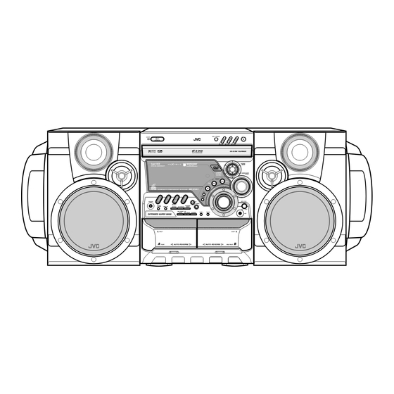
MX-DVA5
STANDBY
STANDBY/ON
PHONES
SELECT
CLOCK
/ TIMER
DISPLAY
REPEAT
REC START
/STOP
SP-MXDVA5
CA-MXDVA5
CD/ DVD Mechanism is exchanged by a unit (contain CPC cords).
1-2
1-3
1-4
1-5
1-17
COPYRIGHT
2001 VICTOR COMPANY OF JAPAN, LTD.
DISC CHANGE
SOUND
MODE
SUBWOOFER
LEVEL
TUNING
CD
TAPE A
TAPE B
REC START
DUBBING
SP-MXDVA5
Adjustment method
Troubleshooting
Description of major ICs
MX-DVA5
Area Suffix
UG
Turkey, South Africa, Egypt
US
Singapore
UW
Brazil, Mexico, Peru
UY
Argentina
PlayBack
Control
VIDEO CD
1-18
1-22
1-25~ 35
No.20966
Jun. 2001
Advertisement
Table of Contents

Related Manuals for JVC MX-DVA5


Summary of Contents for JVC MX-DVA5
- Page 1 MX-DVA5 SERVICE MANUAL COMPACT COMPONENT SYSTEM MX-DVA5 Area Suffix Turkey, South Africa, Egypt Singapore Brazil, Mexico, Peru Argentina DISC CHANGE STANDBY STANDBY/ON SOUND MODE SUBWOOFER LEVEL PHONES TUNING SELECT CLOCK / TIMER DISPLAY REPEAT REC START TAPE A TAPE B...
- Page 2 MX-DVA5 1. This design of this product contains special hardware and many circuits and components specially for safety purposes. For continued protection, no changes should be made to the original design unless authorized in writing by the manufacturer. Replacement parts must be identical to those used in the original circuits. Services should be performed by qualified personnel only.
-
Page 3: Important For Laser Products
MX-DVA5 Important for laser products 5.CAUTION : If safety switches malfunction, the laser is able 1.CLASS 1 LASER PRODUCT to function. 2.DANGER : Invisible laser radiation when open and inter 6.CAUTION : Use of controls, adjustments or performance of lock failed or defeated. Avoid direct exposure to beam. -
Page 4: Preventing Static Electricity
MX-DVA5 Preventing static electricity 1. Grounding to prevent damage by static electricity Electrostatic discharge (ESD), which occurs when static electricity stored in the body, fabric, etc. is discharged, can destroy the laser diode in the traverse unit (optical pickup). Take care to prevent this when performing repairs. -
Page 5: Disassembly Method
MX-DVA5 Disassembly method Metal cover <Main body> Removing the metal cover (See Fig.1 and 2) Remove the three screws A attaching the metal cover on the back of the body. Remove the six screws B attaching the metal cover on both sides of the body. - Page 6 MX-DVA5 FLdispaly & system control board UCW3 Front panel assembly Rear panel Fig.4 Fig.5 Adhesive card wire strap CD/ DVD changer unit CD/ DVD changer unit Rear panel Rear panel Fig.6a Fig.6b Front panel assembly Removing the front panel assembly (See Fig.7 to 9 )
- Page 7 MX-DVA5 Front panel assembly Joint b Joint b Main board Bottom side Joint c Fig.8 Removing the heat sink, AMP board and Fig.9 DVD power board (See Fig.10 to 12) Prior to performing the following procedure, remove the metal cover and the CD/ DVD changer unit.
- Page 8 MX-DVA5 Removing the tuner board (See Fig.11 and 13) Rear panel Prior to performing the following procedure, remove the metal cover and CD/ DVD changer unit. CON01 Disconnect the card wire from connector CON01 on the tuner board. Remove the two screws L attaching the tuner board.
- Page 9 MX-DVA5 Removing the power ICs and DVD power Heat sink board (See Fig.16 and 17) Prior to performing the following procedure, remove the metal cover, CD/ DVD changer unit, heat sink, DVD power board AMP board and DVD power board.
- Page 10 MX-DVA5 <Front panel assembly> Power / DVD switch board UCW1 Prior to performing the following procedure, remove the metal cover, the CD/ DVD changer unit and the Tab c front panel assembly. FL diplay & system Removing the power / DVD switch board...
- Page 11 MX-DVA5 <CD/ DVD changer unit> DVD tray Loading pulley Prior to performing the following procedure, remove gear the CD/ DVD changer unit. Removing the DVD tray (See Fig.1 to 3) Disconnect the card wire from connector SCW1 of the CD servo board.
- Page 12 MX-DVA5 Removing the sensor board / the turn table motor assembly (See Fig.6 to 8) Prior to performing the following procedure, remove Tab b the CD tray. Remove the screw A attaching the sensor board and release the two tabs b attaching the sensor board on the under side of the DVD tray.
- Page 13 MX-DVA5 CD/ DVD servo board SCW1 Fig.10 Removing the CD/ DVD mechanism holder assembly (mechanism included) CD/ DVD mechanism holder assembly (See Fig.11 to 13) Disconnect the card wire from connector CN5 on the motor board in the CD mechanism holder assembly on the under side of the CD changer unit.
-
Page 14: Cassette Mechanism Section
MX-DVA5 R/P Head <Cassette mechanism section> Removing the record/playback mechanism. Removing the R/P head. Remove the screw A on the right side of the R/P head.(Fig.1) Remove the screw B on the left side of the R/P head.(Fig.1) Stopper Pinch roller assembly Removing the pinch roller. - Page 15 MX-DVA5 Motor Removing the motor. Mecha. terminal board Remove the two screws C fixing the motor. Be careful to grease's splash when the drive belt comes off.(Fig.4, Fig.5) Unsolder the motor terminal.(Fig.4) Removing the mechanism board. Unsolder the four parts a on the solenoid...
- Page 16 MX-DVA5 < Speaker section > Removing the side panel (See Fig. 1) Side panel Remove the five screws A and B attaching the side panel, then remove the side panel. Fig.1 Side speaker Removing the side speaker (See Fig. 2 and 3)
-
Page 17: Wiring Connection
MX-DVA5 Wiring connection Color codes are shown below. Brown Orange Yellow Green Blue Violet Gray White Black 3809-001185 AH39-00097A AH39-00097A AH39-00022A CW302 AH39-00202A CW301 1-17... -
Page 18: Adjustment Method
MX-DVA5 Adjustment method 1. Tuner * Adjustment Location of Tuner PCB LW OSC AM(MW) RF AM(MW) RF AM(MW) OSC Adjustment Adjustment Adjustment Adjustment ITEAM Received FREQ. 594 KHz 146~290 KHz 150 KHz 522~1611 KHz Adjustment point Maximum Maximum 2~7.0 1~7.0... - Page 19 MX-DVA5 FM THD Adjustment Output Antenna SSG FREQ. Terminal 98 MHz Oscilloscope FM S.S.G Adjustment Input point FM DETECTOR COIL Speaker (FM DET) Terminal output Input 60 dB Output Distortion Meter Minumum Distortion (0.4% below) (Figure 1-1) Figure1-1 IF CENTER and THD Adjustment...
- Page 20 MX-DVA5 2 Cassette Deck 2-1 To Adjust Tape Speed Notes Cassette Deck Frequency Counter 1) Measuring tape : VT712(or equivalent) SPK OUT (Tapes recorded with 3kHz) output 2) Connect the cassette deck to the frequency counter as in figure 1-5.
- Page 21 MX-DVA5 2-2 T o Adjust PlayBack Level/REC Notes 1) Before the actual adjustment, clean the play/recording head. 2) Measuring tape : i) VT-703 (or equivalent 10kHz AZIMUTH control) ii) AC-225 3) The cassette deck is connections as shown in figure 1-7.
-
Page 22: Troubleshooting
MX-DVA5 Troubleshooting 1.Amplifier Power Malfunction No Output 1-22... - Page 23 MX-DVA5 2.T uner Malfunction(FM/AM) 3.T ape 1-23...
- Page 24 MX-DVA5 4.CD Is state of rotation proper? Is signal of RAO proper? (#2, #3, #4, #5 of WIC101) 1-24...
-
Page 25: Description Of Major Ics
MX-DVA5 Description of major ICs 74HCU04 (VIC6) : Optical BA4560 (FIC2, FIC4, FIC5, HIC1, JIC2) : OP amp. 1. Pin configuration. 1.Pin layout 1A 1 14 Vcc 1Y 2 13 6A OUT1 2A 3 12 6Y 2Y 4 11 5A –... - Page 26 MX-DVA5 BA7660FS (VIC8) : 3 channel 75 driver 1. Block diagram MUTE OUTA1 OUTA2 OUTB1 OUTB2 N.C. N.C. OUTC1 OUTC2 2. Pin function Pin No. Pin Name Comment MUTE Mute Control Terminal This pin supplying "H" voltage 3 channel mute operate.
- Page 27 MX-DVA5 TC7S08F (DIC7, VIC3) : 2 Input and gate 1. Pin layout 2. Block diagram IN B IN A OUT X KA22291(JIC1) : RB/REC PRE amp. 1.Pin layout KA22291 1 2 3 4 5 6 7 8 9 10 11 12 2.Block diagram...
- Page 28 MX-DVA5 KA3082 (LIC1, LIC2) : Bi-directional DC motor driver 1.Pin layout KA3082 2.Pin function Pin Nu mber Pin Name Pin Fun ction Descriptio n Ground Output 1 Phase compensation Motor speed control Input 1 Input 2 Supply voltage (Signal) Supply voltage (Power)
- Page 29 MX-DVA5 L4959 (RIC1) : Voltage regulator 1.Pin layout OUT 12V(a) OUT 8.6V EN 8.6V EN 12V(a) EN 12V(b) N.C. OUT 5.6V OUT 12V(b) TAB CONNECTED TO PIN 6 D97AU716A 2.Block diagram 2/10 5.6V, 250mA OUT 5.6V REGULATOR 8.6V, 600mA OUT 8.6V...
- Page 30 MX-DVA5 M65855FP(EIC1) : Sound processor 2. Pin function 1. Pin layout Pin No. Symbol DESCRIPTION CLOCK Echo level control with external DC voltage ECHOVOL ECHOVOL ECHOMUTE To connect 1/2 Vcc output and filter capacitor V CC OP2 IN Uses external C to from an D/A conversion...
- Page 31 MX-DVA5 M66010 (UIC2) : I/O control 1.Pin layout 2.Block diagram Shift register 1 SERIAL DATA OUTPUT D24 D23 D22 D3 D2 D1 CLOCK INPUT SET INPUT CHIP SELECT Q24 Q23 Q22 Q3 Q2 Q1 PARALLEL INPUT Parallel output latch DATA I/O...
- Page 32 MX-DVA5 TDA7442D (FIC1) : Audio processor 1.Pin layout R_IN3 R_IN4 R_IN2 LOUT R_IN1 ROUT L_IN1 AGND L_IN2 L_IN3 CREF L_IN4 MUXOUTL IN(L) DIG-GND MUXOUT(R) TREBLE(R) IN(R) TREBLE(L) BIN(R) BOUT(R) BIN(L) BOUT(L) 2.Block diagram 5.6K 5.6nF 100nF 100nF 100nF 2.2 F...
- Page 33 MX-DVA5 ZIVA-3 (VIC1) : AV Decoder 1.Terminal Layout 2.Block Diagrams DRAM/ 208 ~ 157 Memory Controller Decoder Interface Video Subpicture Mixer Decoder Host Host Video Interface Interface MPEG Interface Control Logic Video Sync Decoder ~ 104 Generator Program DVD/CD Stream...
- Page 34 MX-DVA5 Pin Function (2/3) Function Symbol Symbol Function Pin No. Pin No. Connect to TP564 Connect to GND E-VSS ARAM-ADDR14 Test pin Address output to IC508,504 TEST-PIN1 M-ADDR11 Data bus I/O to IC508,IC504 Address output to IC508,504 M-ADDR8 M-DATA15 Data bus I/O to IC508,IC504...
- Page 35 MX-DVA5 Pin Function (3/3) Function Symbol Symbol Function Pin No. Pin No. Connect to TP507 DVD image signal output A-VDD VDATA1 Dot clock signal output (27MHz) Power supply I-VDD VCLK Connect to TP505 DVD image signal output SYSCLK VDATA2 Connect to GND...
- Page 36 MX-DVA5 VICTOR COMPANY OF JAPAN, LIMITED AUDIO & COMMUNICATION BUSINESS DIVISION PERSONAL & MOBILE NETWORK BUSINESS UNIT. 10-1,1chome,Ohwatari-machi,Maebashi-city,371-8543,Japan (No.20966) 200106(V)
Need help?
Do you have a question about the MX-DVA5 and is the answer not in the manual?
Questions and answers