Sony MVC-FD83 Service Manual
Hide thumbs
Also See for MVC-FD83:
- Operating instructions manual (133 pages) ,
- Service manual (113 pages) ,
- User manual (2 pages)
Table of Contents
Advertisement
Quick Links
SERVICE MANUAL
Ver 1.0 1999. 05
This service manual contains information
for Japanese model as well.
MICROFILM
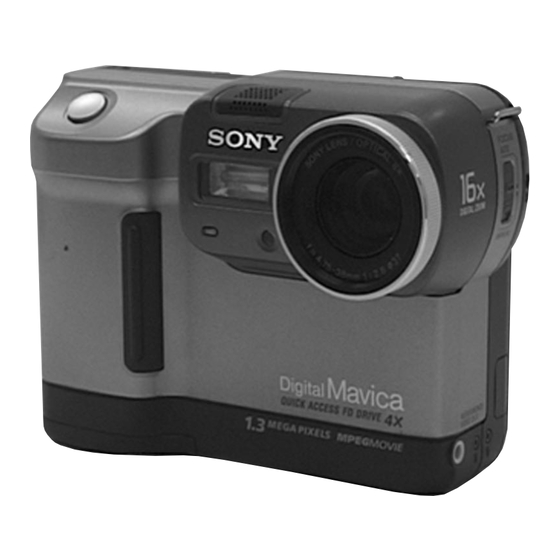
MVC-FD83/FD88
Photo: MVC-FD88
SPECIFICATIONS
US Model
Canadian Model
AEP Model
UK Model
Australian Model
Hong Kong Model
Chinese Model
Korea Model
MVC-FD83/FD88
Tourist Model
DIGITAL STILL CAMERA
E Model
MVC-FD88
Advertisement
Table of Contents

Related Manuals for Sony MVC-FD83


Summary of Contents for Sony MVC-FD83
- Page 1 MVC-FD83/FD88 SERVICE MANUAL US Model Canadian Model AEP Model UK Model Ver 1.0 1999. 05 E Model Australian Model Hong Kong Model Chinese Model Korea Model MVC-FD83/FD88 Tourist Model Photo: MVC-FD88 MVC-FD88 This service manual contains information for Japanese model as well.
- Page 2 MVC-FD83/FD88 CD-228 (CCD IMAGER) PRINTED WIRING BOARD AND SCHEMATIC DIAGRAM 4-2. PRINTED WIRING BOARDS AND SCHEMATIC DIAGRAMS – Ref. No.: CD-228 board; 2,000 series – THIS NOTE IS COMMON FOR WIRING BOARDS AND SCHEMATIC DIAGRAMS – MVC-FD88 – (In addition to this, the necessary note is printed in each block) •...
-
Page 3: Ccd Imager
MVC-FD83/FD88 CD-229 (CCD IMAGER) PRINTED WIRING BOARD AND SCHEMATIC DIAGRAM – Ref. No.: CD-229 board; 2,000 series – – MVC-FD83 – • For Printed Wiring Board. • CD-229 board is 4-layer print board. However, the patterns of layers 2 to 3 have not been included in the diagram. - Page 4 MVC-FD83/FD88 FC-70 (CAMERA SIGNAL PROCESS) SCHEMATIC DIAGRAM • See page 4-9 for FC-70 printed wiring board. FC-70 BOARD (1/10) 4.8 Vp-p 41 nsec IC003 @∞ REC/PB 4.0 Vp-p 24.545451 MHz: NTSC 24.375 MHz: PAL IC003 @§ REC/PB 4.0 Vp-p 83 nsec IC003 #º...
- Page 5 MVC-FD83/FD88 FC-70 (CAMERA DSP, VIDEO DECODER) SCHEMATIC DIAGRAM • See page 4-9 for FC-70 printed wiring board. FC-70 BOARD (2/10) 460 mVp-p Q202 B REC/PB (A/V OUT jack used) !º 420 mVp-p Q203 B REC/PB !¡ 210 mVp-p Q204 B REC/PB !™...
- Page 6 MVC-FD83/FD88 FC-70 (LENS MOTOR DRIVE) SCHEMATIC DIAGRAM • See page 4-9 for FC-70 printed wiring board. LENS MOTOR DRIVE FC-70 (3/10) 4-20 4-21 4-22...
-
Page 7: Audio Interface
MVC-FD83/FD88 MVC-FD83/FD88 FC-70 (AUDIO INTERFACE) SCHEMATIC DIAGRAM • See page 4-9 for FC-70 printed wiring board. FC-70 BOARD (4/10) !£ 4.0 Vp-p 16.384 MHz IC503 $¡ REC/PB AUDIO INTERFACE FC-70 (4/10) 4-23 4-24... -
Page 8: Media Control
MVC-FD83/FD88 FC-70 (MEDIA CONTROL) SCHEMATIC DIAGRAM • See page 4-9 for FC-70 printed wiring board. FC-70 BOARD (5/10) !¢ 1.6 Vp-p 12.9024 MHz IC401 !¢ REC/PB MEDIA CONTROL FC-70 (5/10) 4-26 4-27 4-28... - Page 9 MVC-FD83/FD88 FC-70 (FD CONTROL) SCHEMATIC DIAGRAM • See page 4-9 for FC-70 printed wiring board. FC-70 BOARD (6/10) !∞ 1.3 Vp-p 48 MHz IC902 %£ REC/PB FD CONTROL FC-70 (6/10) 4-29 4-30 4-31...
-
Page 10: Mode Control
MVC-FD83/FD88 FC-70 (MODE CONTROL) SCHEMATIC DIAGRAM • See page 4-9 for FC-70 printed wiring board. FC-70 BOARD (7/10) !§ 3.2 Vp-p 20 MHz IC303 $¡ REC/PB !¶ 3.2 Vp-p IC303 ^™ REC/PB !• 700 mVp-p 32.768 kHz IC306 3 REC/PB !ª... - Page 11 MVC-FD83/FD88 MVC-FD83/FD88 FC-70 (A/V OUT) SCHEMATIC DIAGRAM • See page 4-9 for FC-70 printed wiring board. FC-70 BOARD (8/10) @º 480 mVp-p IC601 !ª REC/PB (A/V OUT jack used) @¡ 540 mVp-p IC601 1 REC/PB (A/V OUT jack used) @™...
-
Page 12: Audio A/D D/A Converter
MVC-FD83/FD88 FC-70 (AUDIO A/D D/A CONVERTER) SCHEMATIC DIAGRAM • See page 4-9 for FC-70 printed wiring board. 4-38 AUDIO A/D D/A CONVERTER FC-70 (9/10) 4-39 4-40... - Page 13 MVC-FD83/FD88 MVC-FD83/FD88 FC-70 (DC/DC CONVERTER) SCHEMATIC DIAGRAM • See page 4-9 for FC-70 printed wiring board. FC-70 BOARD (10/10) @£ 1.9 Vp-p 2 µsec IC801 $§ REC/PB @¢ 1.1 Vp-p 2 µsec IC801 $¢ REC/PB @∞ 1.0 Vp-p 2 µsec IC801 $º...
-
Page 14: Rec/Pb Amp, Motor Drive
MVC-FD83/FD88 PK-47/48 (REC/PB AMP, MOTOR DRIVE) SCHEMATIC DIAGRAMS • See page 4-45 for PK-47/48 printed wiring board. PK-47/48 BOARD (1/5) 4.0 Vp-p 4 MHz IC601 @∞ REC/PB 4-51 REC/PB AMP, MOTOR DRIVE PK-47/48 (1/5) 4-49 4-50... - Page 15 MVC-FD83/FD88 PK-47/48 (LCD DRIVE) SCHEMATIC DIAGRAM • See page 4-45 for PK-47/48 printed wiring board. PK-47/48 BOARD (2/5) 580m Vp-p IC802 8 REC/PB 460m Vp-p IC802 9 REC/PB 220 mVp-p IC802 !º REC/PB 4.4 Vp-p IC802 @º REC/PB 4.4 Vp-p IC802 @™...
-
Page 16: Timing Generator
MVC-FD83/FD88 PK-47/48 (TIMING GENERATOR) SCHEMATIC DIAGRAM • See page 4-45 for PK-47/48 printed wiring board. PK-47/48 BOARD (3/5) 3.2 Vp-p IC901 #¶ REC/PB 2.4 Vp-p IC901 #¢ REC/PB !º 3.8 Vp-p 150 nsec IC901 @§ REC/PB TIMING GENERATOR PK-47/48 (3/5) - Page 17 MVC-FD83/FD88 MVC-FD83/FD88 PK-47/48 (MODE SWITCH) SCHEMATIC DIAGRAM • See page 4-45 for PK-47/48 printed wiring board. MODE SWITCH PK-47/48 (4/5) 4-59 4-60...
- Page 18 MVC-FD83/FD88 PK-47/48 (BACK LIGHT DRIVE) SCHEMATIC DIAGRAM • See page 4-45 for PK-47/48 printed wiring board. PK-47/48 BOARD (5/5) !¡ 6.0 Vp-p 2 µsec IC851 1 REC/PB BACK LIGHT DRIVE PK-47/48 (5/5) 4-61 4-62 4-63...
- Page 19 MVC-FD83/FD88 RL-54/56 (RELEASE SWITCH) PRINTED WIRING BOARD AND SCHEMATIC DIAGRAM FU-135/137 (DC IN) PRINTED WIRING BOARD AND SCHEMATIC DIAGRAM – Ref. No.: RL-54/56 board; 2,000 series – – Ref. No.: FU-135/137 board; 2,000 series – • For Printed Wiring Board.
Need help?
Do you have a question about the MVC-FD83 and is the answer not in the manual?
Questions and answers