Table of Contents
Advertisement
EMX5000-12/20
SERVICE MANUAL
本资料由OKXIA视听皮带资源库www.okxia.cn提供
EMX5000-20
CONTENTS
................................................ 3/5
.................................... 7
............... 11
BLOCK & LEVEL DIAGRAM ....................................................... 12
................................................................... 14
.......................................................... 14
............................ 15
.............................. 20
................................. 23
CIRCUIT BOARDS
....................................... 24
INSPECTIONS
...................................................... 39/46
............................................. 54
This document is printed on chlorine free (ECF) paper with soy ink.
011633
PA
HAMAMATSU, JAPAN
1
1.387K-9551
Printed in Japan 2002.3
Advertisement
Table of Contents

Related Manuals for Yamaha EMX5000-12


Summary of Contents for Yamaha EMX5000-12
- Page 1 EMX5000-12/20 SERVICE MANUAL 本资料由OKXIA视听皮带资源库www.okxia.cn提供 EMX5000-20 CONTENTS SPECIFICATIONS ..........3/5 PANEL LAYOUT ........7 CIRCUIT BOARD LAYOUT ....11 BLOCK & LEVEL DIAGRAM ............12 WIRING ..............14 DIMENSIONS ............14 DISASSEMBLY PROCEDURE ......15 LSI PIN DESCRIPTION ......20 IC BLOCK DIAGRAM .........
-
Page 2: Specifications
IMPOR TANT NOTICE This manual has been provided for the use of authorized Yamaha Retailers and their service personnel. It has been assumed that basic service procedures inherent to the industry, and more specifically Yamaha Products, are already known and under- stood by the users, and have therefore not been restated. - Page 3 230 V AC 50 Hz, 550 W Power consumption Other: 240 V AC 50 Hz, 550 W 682 × 158 × 538 mm (EMX5000-20) / 478 × 158 × 538 mm (EMX5000-12) Dimensions (WxHxD) Weight 19 kg (EMX5000-20) / 15 kg (EMX5000-12) Accessories Power cord, Owner’s Manual...
- Page 4 EMX5000-12/20 Input specifications Input level Gain Actual load For use with Connectors on Input terminals control impedance nominal mixer Nominal Max. before clip Sensitivity –60 –80 dB (0.078 mV) –60 dB (0.775 mV) –40 dB (7.75 mV) CH INPUT A 5 kΩ...
- Page 5 EMX5000-12/20...
- Page 6 EMX5000-12/20...
-
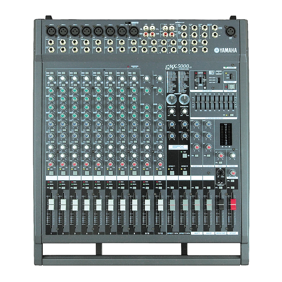
Page 7: Panel Layout
80 (High pass filter) switch Equalizer controls (HIGH, MID, LOW) AUX1, AUX2 controls / POST switches EFF 1, 2 controls (EFFECT) PAN (panpot) control (EMX5000-20: Cannels 1-16, EMX5000-12: Cannels 1-8) BAL (balance) control (EMX5000-20: Cannels 17/18-19/20, EMX5000-12: Cannels 9/10-11/12) ON switch, indicator PEAK indicator... - Page 8 EMX5000-12/20 Stereo Sub Input Section AUX 1, 2 controls ST (stereo) control PFL (pre-fader listen) switch Master Control Section AUX 1 fader AUX 2 fader MONO OUT fader ST OUT fader AFL (after fader listen) switch 2TR IN Section ST (stereo) control...
- Page 9 EMX5000-12/20 Digital effect Section PROGRAM selector PARAMETER control AUX 1/2 control TAP switch, indicator EFFECT 1/2 ON switch PFL (Pre-fader listen) switch EFFECT 1/2 RTN fader Graphic equalizer Section Power amp Section LIMITER indicator Power amp select switch Graphic equalizer...
- Page 10 ON/OFF switch STAND-BY ON/OFF switch Input/Output pabel ! 5 ! 6 ! 7 Channel input jacks (INPUT A, INPUT B) EMX5000-20: 1–16, EMX5000-12: 1–8 INSERT I/O (insert) jacks PHANTOM switch LINE (stereo) input jacks EMX5000-20: 17/18–19/20, EMX5000-12: 9/10–11/12 2TR IN jacks...
-
Page 11: Circuit Board Layout
EMX5000-12/20 Rear panel AC inlet POWER switch SPEAKERS (speaker output) jacks CIRCUIT BOARD LAYOUT SMPS 1/2 SMPS 2/2 EMX5000-20 only IN16... - Page 12 EMX5000-12/20 BLOCK & LEVEL DIAGRAM IN8/IN16 +48V PHANTOM 8CH/SW PEAK CH INPUT EMX5000-12:[CH1-8] STAND-BY EMX5000-20:[CH1-8] [CH9-16] SIGNAL IC107,307, CN903, 904 [–60~–16dB] IC101,201,301,401,501,601,701,801 [–34~+10dB] 507,707 [0dB] CH Fader [0dB] EMX5000-12:CH1-8 [0dB] [0dB] [–10dB] EMX5000-12:CH1-8 EMX5000-20:CH1-16 3-Stage EQ IC302 EMX5000-20:CH1-16 [0dB] 26dB...
- Page 13 EMX5000-12/20 IC316 JK301 [–6dB] STAND-BY IC316 JK505 ST SUB OUT ST SUB OUT JK302 [+4dB] EMX5000-12:CH1-8 REC OUT EMX5000-20:CH1-16 [–10dBV] [0dB] IC303 IC317 [0dB] [0dB] JK303 [–10dB] MAIN GEQ Q303 9-Stage GEQ [0dB] ST OUT ST OUT CN602 CN105 CN102 VH3P...
-
Page 14: Wiring
CN101 CN105 SMPS CN103 Coil W101 CN102 CN102 Connector assembly Cord holder Connector assembly CN103 Connector assembly AC shield CN104 Connector assembly SMPS W102 Connector assembly H, B, W, K DC FAN BOTTOM ASSY DIMENSIONS (EMX5000-20) 478 (EMX5000-12) Units: mm... -
Page 15: Disassembly Procedure
[160b], three (3) screws marked [170a] and four (4) screws marked [170b] (three (3) for EMX5000-12), Then lift the front end of the panel assembly, turn it about 45° and remove the panel assembly by releasing it from the claws on its side. - Page 16 EMX5000-12/20 Coil (Time required: about 6 minutes) 2-1. Remove the panel assembly. (See Procedure 1.) 2-2. After removing the two (2) screws marked [B250], remove the harness and then the coil. (Fig. 2) DC fan (Time required: about 7 minutes) 3-1.
- Page 17 (3) hexagon socket head screws marked [P38a]. The MAS circuit board can then be removed. (Fig. 4) IN8/IN16 Circuit Board: CH1-8 / EMX5000-12, CH9- 18 / EMX5000-20 (Time required: about 40 minutes) 6-1. Remove the panel assembly. (See Procedure 1.) 6-2.
- Page 18 EMX5000-12/20 [B90] [B90] [P240] DSP-SPX [P220] [B90] [B90] [B90]: Bind Head Tapping Screw-B 3.0X6 MFZN2BL (EP600230) Fig.3 [P70d] [P70c] [P70b] [P60a] [P70a] [P60c] [P60a] [P38a] [P38b] [P38b] [P38b] [P38c] [P38c] [P38c] [P60a] [P60b] [P60b] IN16 [P38]: Screw 3X6 MFZNBL (V9156000) [P60]: Screw 3X25 MFZNBL (V3289800) [P70]: Bonding Tapping Screw-B 3.0X8 MFZN2BL (VN413300)
- Page 19 EMX5000-12/20 PWR Circuit Board (Time required: about 30 minutes) 8-1. Remove the panel assembly. (See Procedure 1.) 8-2. Remove the thirty-four (34) transistor fixing screws marked [B60], four (4) PWR circuit board fixing screws marked [B50] from the PWR assembly, four (4) screws marked [85] and two (2) hexagonal nuts from the rear panel.
-
Page 20: Lsi Pin Description
EMX5000-12/20 LSI PIN DESCRIPTION YSS910-S (XV988A00) DSP6 (Digital Signal Processor) DSP-SPX: IC112 NAME FUNCTION NAME FUNCTION Power supply (3.3 V) Ground Ground DB13 System master clock input (60 MHz or 30 MHz) DB14 System master clock output (High or 30 MHz) - Page 21 EMX5000-12/20 YM3436DK (XG948E0) DIR2 (Digital Format Interface Receiver) DSP-SPX: IC103 NAME FUNCTION NAME FUNCTION DAUX Auxiliary input for audio data RSTN System reset input HDLT Asynchronous buffer operation flag Vdda VCO section power (+5V) DOUT Audio data output CTLN VCO control input N...
- Page 22 EMX5000-12/20 M30622MCA-XXXFP (X2416A00) CPU DSP-SPX: IC109 NAME FUNCTION NAME FUNCTION P96/ I/O/O P46/CS2 P95/ P45/CS1 I/O/O P94/ P44/CS0 I/O/O This is an 8-bits I/O port. I/O/O P93/ P43/A19 P92/ P42/A18 I/O/O P91/ P41/A17 I/O/O This is an 8-bits I/O port.
-
Page 23: Ic Block Diagram
EMX5000-12/20 IC BLOCK DIAGRAM 74HC08DT(XZ108A00) LB1412M (XT547A00) 74HCU04DT (XZ110A00) LED DRIVER INVERTER DSP-SPX: IC111 DSP-SPX: IC104 MAS: IC601, IC602 OUT1 OUT2 RESET NJM2060(TE2) (XM560A00) NJM2068MD-T1 (XJ553A00) NJM4556AL XP844A00 OP AMP OP AMP OP AMP IN8: IC101-105,IC107, IC201, IC301-305, MAS: IC311-315... - Page 24 INPUT 2/10 3/11 4/12 5/13 6/14 7/15 8/16 INPUT A INPUT B INSERT PHANTOM GAIN HIGH MID-f...
- Page 25 HIGH MID-f AUX1 POST AUX2 POST EFFECT1 EFFECT2 ON/OFF...
- Page 26 EFFECT2 ON/OFF PEAK SIGNAL CN904: CN902: (EMX5000-20) (EMX5000-20) to othere IN8 CN902 from IN8 or MAS CN604 (EMX5000-12) (EMX5000-12) N.C. to MAS CN604 FADER CN901: CN903: (EMX5000-26) (EMX5000-20) from IN8 to othere IN8 CN901 (EMX5000-12) or MAS CN603 N.C. (EMX5000-12)
- Page 30 CN501: CN601: to DSP to PWR CN101 LINE17 L LINE19 L 2TR IN L REC OUT L AUX SEND1 ST OUT L ST SUB L EFFECT ON/OFF LINE18 R LINE20 R 2TR IN R REC OUT R AUX SEND2 ST OUT R ST SUB R LAMP CN602:...
- Page 31 POWER 500W/ STAND-BY 300W/100W HIGH PROGRAM MAIN PARAMETER EQ ON/OFF AUX1 AUX1 POST INDICATORS AUX2 AUX2 POST EFFECT1 EFFECT2 PHONES 2TR IN...
- Page 32 2TR IN ON/OFF ST SUB OUT LPF-f EFFECT ON/OFF EFFECT2 ON/OFF PEAK SIGNAL LPF OFF/ON CN604: to IN8 CN904 CN603: to IN8 CN903 9/10 (EMX5000-12) 11/12 (EMX5000-12) EFFECT1 RTN EFFECT2 RTN AUX1 AUX2 MONO OUT ST OUT 17/18 (EMX5000-20) 19/20 (EMX5000-20)
-
Page 36: Circuit Boards
EMX5000-12/20 SMPS 1/2 Circuit Board to coil AC IN POWER ON/OFF Component side SMPS 2/2 Circuit Board CN104: to PWR CN101 C139 Component side to PWR CN105 SMPS: 3NA-V826930... - Page 37 EMX5000-12/20 CN102: to SMPS2/2 W102BL, W102RE, PWR Circuit Board W102BE CN101: SPEAKERS to MAS CN601 CN103: CN105: to SMPS2/2 to MAS CN602 CN104 CN104: Component side to FAN PWR: 3NA-V826960...
- Page 38 EMX5000-12/20 DSP-SPX Circuit Board N.C. CN101: to MAS CN501 Component side Pattern side DSP-SPX: 3NA-V826730...
- Page 39 40 (3W or more) LAMP 30 (20W or more) 600 Ω Other output terminals • Unless otherwise specified, set the controls as follows. 1-1 CH INPUT (1-8: EMX5000-12/1-16: EMX5000-20) 26dB switch GAIN control MINIMUM HPF switch EQ(HIGH, MID, LOW) level control...
- Page 40 +1 ± 2 +20.8 ± 2 -11 ± 2 INSERT IN *1: Turn on the PFL switch of the channel to which the signal was input. [Table 2-3] Input terminal [ST INPUT CH9-12: EMX5000-12 / 17-20: EMX5000-20] [Unit: dBs] INPUT INPUT GAIN...
- Page 41 +12 ± 2 MAX. – HIGH 100Hz -12 ± 2 MIN. – [Table 4-2] Input terminal [ST INPUT, CH9-12: EMX5000-12 / CH17-20: EMX5000-20] [Unit: dBs] level control Input frequency Variation width +12 ± 2 MAX. 100Hz -12 ± 2 MIN.
- Page 42 EMX5000-12/20 GRAPHIC EQUALIZER CHARACTERISTICS • In the state as described in 1, move the GEQ fader to the MIN or MAX position and check that the output level of the frequency obtained at ST1 OUT (L, R) falls within the range given in Table 5-1 with the output level obtained at the center click position used as a reference.
- Page 43 Unless otherwise specified, the load resistance of the speakers should be connected only when checking the power amplifier. • Set INPUT CH1-20 (EMX5000-20) / CH1 – 12 (EMX5000-12), ST SUB IN 2 and 2TR IN level controls to the MIN position.
- Page 44 • YAMAHA SPEAKERS PROCESSING switch ON Input 70Hz/-19dBs signal to the input terminal and check that the output voltage when YAMAHA SPEAKERS PROCESSING switch is turned off is within the range of +6.2±2dB with 1kHz output voltage used as a reference.
- Page 45 • EQ (GAIN), GEQ, PAN, BAL CENTER • PROGRAM select • All VR/FADER controls other than above MINIMUM • All push switches OFF (light off) • PHANTOM switch • SIGNAL SELECT switch MAIN (L, R) • POWER SELECT switch 500W+500W • YAMAHA SPEAKER PROCESSING switch...
- Page 46 EMX5000-12/20...
- Page 47 EMX5000-12/20...
- Page 48 EMX5000-12/20...
- Page 49 EMX5000-12/20...
- Page 50 EMX5000-12/20...
- Page 51 EMX5000-12/20...
- Page 52 EMX5000-12/20...
- Page 53 EMX5000-12/20...
-
Page 54: Parts List
PARTS LIST CONTENTS OVERALL ASSEMBLY ..........2 ELECTRICAL PARTS ..........6 Notes : DESTINATION ABBREVIATIONS A : Australian model M : South African model B : British model O : Chinese model C : Canadian model Q : South-east Asia model D : German model T : Taiwan model E : European model... - Page 55 E M X 5000-12/ 20 OVE R AL L AS S E M B L Y P 100 P 70 P 110 P 120 P 130 P 100 P 10 P 38 P 140 P 150 P 70 P 60 P 130 P 90 P 100...
- Page 56 EMX5000-20 A (V849380) Overall Assembly EMX5000-20 K (V945780) Overall Assembly EMX5000-12 J (V821180) Overall Assembly EMX5000-12 U,V (V821190) Overall Assembly EMX5000-12 H,B,W (V821210) Overall Assembly EMX5000-12 A (V821220) Overall Assembly EMX5000-12 K (V945720) VV104600 Cord Holder CV-100 Name Plate KOREA...
- Page 57 EMX5000-12/20 PART NO. DESCRIPTION REMARKS REF NO. RANK B70a AAX33190 Circuit Board SMPS 1/2 (V826930,X0627B0) B70a AAX33200 Circuit Board SMPS 1/2 (V826940,X0627B0) B70a AAX33210 Circuit Board SMPS 1/2 H,B,W,K (V826950,X0627B0) * B70a AAX71680 Circuit Board SMPS 1/2 (X848520,X0627B0) B70b AAX74520...
- Page 58 V 2 9 4 7 0 0 0 Fader Knob BLACK/N-GRAY EMX5000-20 FADER(CH1-20) P150 V 2 9 4 7 0 0 0 Fader Knob BLACK/N-GRAY EMX5000-12 FADER(CH1-12) P160 V 6 6 2 3 3 0 0 Fader Knob D-RED/CD-GRAY FADER(EFFECT1 RTN,EFFECT2 RTN,AUX1,AUX2) P170...
- Page 59 EMX5000-12/20 ELECTRICAL PARTS PART NO. DESCRIPTION REMARKS REF NO. RANK ELECTORICAL PARTS AAX33240 Circuit Board DSP-SPX PRESTO (V826730,X2259B0) V 8 2 6 7 4 0 0 Circuit Board (X0655B0) V 9 0 9 3 1 0 0 Cirsuit Board IN16...
- Page 60 EMX5000-12/20 PART NO. DESCRIPTION REMARKS REF NO. RANK C189 UR838100 Electrolytic Cap. 100.00 16.0V C190 UX145100 Ceramic Capacitor (Chip) 0.1000 25V Z -200 UX145100 Ceramic Capacitor (Chip) 0.1000 25V Z C201 UX063100 Ceramic Capacitor (Chip) 1000P 50V K C202 UX063100...
- Page 61 EMX5000-12/20 PART NO. DESCRIPTION REMARKS REF NO. RANK Q304 VD303700 Transistor 2SC3326 A,B TE85R R101 RG000000 Carbon Resistor (chip) 0 0.1 J R102 RG000000 Carbon Resistor (chip) 0 0.1 J R107 RG006330 Carbon Resistor (chip) 3.3K 0.1 J R108 RG005470 Carbon Resistor (chip) 470 0.1 J...
- Page 62 EMX5000-12/20 PART NO. DESCRIPTION REMARKS REF NO. RANK R347 RG006470 Carbon Resistor (chip) 4.7K 0.1 J R348 RG006470 Carbon Resistor (chip) 4.7K 0.1 J R349 RG004330 Carbon Resistor (chip) 33 0.1 J R350 RG006470 Carbon Resistor (chip) 4.7K 0.1 J...
- Page 63 EMX5000-12/20 PART NO. DESCRIPTION REMARKS REF NO. RANK C138 UX062100 Ceramic Capacitor (Chip) 100P 50V J C139 UX062100 Ceramic Capacitor (Chip) 100P 50V J C140 UX061470 Ceramic Capacitor (Chip) 47P 50V J C141 UR847470 Electrolytic Cap. 47.00 25.0V C142 UR877100 Electrolytic Cap.
- Page 64 EMX5000-12/20 PART NO. DESCRIPTION REMARKS REF NO. RANK C324 UA953390 Mylar Capacitor 3900P 50V J C325 UX062100 Ceramic Capacitor (Chip) 100P 50V J C326 UA954100 Mylar Capacitor 0.0100 50V J C327 UX061220 Ceramic Capacitor (Chip) 22P 50V J C328 UR847470 Electrolytic Cap.
- Page 65 EMX5000-12/20 PART NO. DESCRIPTION REMARKS REF NO. RANK C510 UX062820 Ceramic Capacitor (Chip) 820P 50V K C511 UX061100 Ceramic Capacitor (Chip) 10P 50V D C512 UX062470 Ceramic Capacitor (Chip) 470P 50V J C513 UX061330 Ceramic Capacitor (Chip) 33P 50V J...
- Page 66 EMX5000-12/20 PART NO. DESCRIPTION REMARKS REF NO. RANK C638 UX062100 Ceramic Capacitor (Chip) 100P 50V J C639 UX062100 Ceramic Capacitor (Chip) 100P 50V J C640 UX061470 Ceramic Capacitor (Chip) 47P 50V J C641 UR847470 Electrolytic Cap. 47.00 25.0V C642 UX064100 Ceramic Capacitor (Chip) 0.0100 50V K...
- Page 67 EMX5000-12/20 PART NO. DESCRIPTION REMARKS REF NO. RANK C824 UA953390 Mylar Capacitor 3900P 50V J C825 UX062100 Ceramic Capacitor (Chip) 100P 50V J C826 UA954100 Mylar Capacitor 0.0100 50V J C827 UX061220 Ceramic Capacitor (Chip) 22P 50V J C828 UR847470 Electrolytic Cap.
- Page 68 EMX5000-12/20 PART NO. DESCRIPTION REMARKS REF NO. RANK JK502 V 3 9 3 9 2 0 0 Phone Jack JY6351J-46-250 2SW INPUT B (CH5) JK503 V 2 8 8 6 0 0 0 Phone Jack JY-6351J-06-340 INSERT (CH5) JK601 V 6 1 2 7 2 0 0...
- Page 69 EMX5000-12/20 PART NO. DESCRIPTION REMARKS REF NO. RANK R101 RG005180 Carbon Resistor (chip) 180 0.1 J R102 VV065300 Metal Film Resistor 6.8K 1/4 F R103 VV065300 Metal Film Resistor 6.8K 1/4 F R104 RF358100 Carbon Resistor (chip) 100.0K : D 1608...
- Page 70 EMX5000-12/20 PART NO. DESCRIPTION REMARKS REF NO. RANK R203 VV065300 Metal Film Resistor 6.8K 1/4 F R204 RF358100 Carbon Resistor (chip) 100.0K : D 1608 R205 RF358100 Carbon Resistor (chip) 100.0K : D 1608 R206 RG007100 Carbon Resistor (chip) 10K 0.1 J...
- Page 71 EMX5000-12/20 PART NO. DESCRIPTION REMARKS REF NO. RANK R307 RF357100 Carbon Resistor (chip) 10.0K : D 1608 R308 RF356110 Carbon Resistor (chip) 1.1K : D 1608 R309 RF357100 Carbon Resistor (chip) 10.0K : D 1608 R310 RF358100 Carbon Resistor (chip) 100.0K : D 1608...
- Page 72 EMX5000-12/20 PART NO. DESCRIPTION REMARKS REF NO. RANK R411 RF358100 Carbon Resistor (chip) 100.0K : D 1608 R412 RG007220 Carbon Resistor (chip) 22K 0.1 J R413 RG006470 Carbon Resistor (chip) 4.7K 0.1 J R414 RF358100 Carbon Resistor (chip) 100.0K : D 1608...
- Page 73 EMX5000-12/20 PART NO. DESCRIPTION REMARKS REF NO. RANK R512 RG007220 Carbon Resistor (chip) 22K 0.1 J R513 RG006470 Carbon Resistor (chip) 4.7K 0.1 J R514 RF358100 Carbon Resistor (chip) 100.0K : D 1608 R515 RF358100 Carbon Resistor (chip) 100.0K : D 1608...
- Page 74 EMX5000-12/20 PART NO. DESCRIPTION REMARKS REF NO. RANK R614 RF358100 Carbon Resistor (chip) 100.0K : D 1608 R615 RF358100 Carbon Resistor (chip) 100.0K : D 1608 R616 RG004100 Carbon Resistor (chip) 10 0.1 J R617 RF356220 Carbon Resistor (chip) 2.2K : D 1608...
- Page 75 EMX5000-12/20 PART NO. DESCRIPTION REMARKS REF NO. RANK R718 RF356820 Carbon Resistor (chip) 8.2K : D 1608 R719 RF354200 Carbon Resistor (chip) 20.0 : D 1608 R720 RF357240 Carbon Resistor (chip) 24.0K : D 1608 R721 RF356220 Carbon Resistor (chip) 2.2K : D 1608...
- Page 76 EMX5000-12/20 PART NO. DESCRIPTION REMARKS REF NO. RANK R822 RF356820 Carbon Resistor (chip) 8.2K : D 1608 R823 RF357240 Carbon Resistor (chip) 24.0K : D 1608 R824 RG004100 Carbon Resistor (chip) 10 0.1 J R825 RF356470 Carbon Resistor (chip) 4.7K : D 1608...
- Page 77 EMX5000-12/20 PART NO. DESCRIPTION REMARKS REF NO. RANK SW402 V 6 9 6 2 6 0 0 Push Switch (CH4) SW403 V 6 9 6 2 6 0 0 Push Switch CH ON(CH4) SW404 V 6 9 6 2 6 0 0...
- Page 78 EMX5000-12/20 PART NO. DESCRIPTION REMARKS REF NO. RANK VR408 V 8 2 6 4 6 0 0 Rotary Variable Resistor A 20.0K XV09213P AUX1(CH4) VR409 V 8 2 6 4 6 0 0 Rotary Variable Resistor A 20.0K XV09213P AUX2(CH4)
- Page 79 EMX5000-12/20 PART NO. DESCRIPTION REMARKS REF NO. RANK -107 UX062820 Ceramic Capacitor (Chip) 820P 50V K C108 UX061100 Ceramic Capacitor (Chip) 10P 50V D C109 UR828470 Electrolytic Cap. 470.00 10.0V C110 UX062820 Ceramic Capacitor (Chip) 820P 50V K C111 UX061100...
- Page 80 EMX5000-12/20 PART NO. DESCRIPTION REMARKS REF NO. RANK C236 UR866470 Electrolytic Cap. 4.70 50.0V C237 UR847100 Electrolytic Cap. 10.00 25.0V C238 UX062100 Ceramic Capacitor (Chip) 100P 50V J C239 UX062100 Ceramic Capacitor (Chip) 100P 50V J C240 UX061470 Ceramic Capacitor (Chip)
- Page 81 EMX5000-12/20 PART NO. DESCRIPTION REMARKS REF NO. RANK C423 UX062100 Ceramic Capacitor (Chip) 100P 50V J C424 UA953390 Mylar Capacitor 3900P 50V J C425 UX062100 Ceramic Capacitor (Chip) 100P 50V J C426 UA954100 Mylar Capacitor 0.0100 50V J C427 UX061220...
- Page 82 EMX5000-12/20 PART NO. DESCRIPTION REMARKS REF NO. RANK C610 UX062820 Ceramic Capacitor (Chip) 820P 50V K C611 UX061100 Ceramic Capacitor (Chip) 10P 50V D C612 UX062470 Ceramic Capacitor (Chip) 470P 50V J C613 UX061330 Ceramic Capacitor (Chip) 33P 50V J...
- Page 83 EMX5000-12/20 PART NO. DESCRIPTION REMARKS REF NO. RANK C740 UX061470 Ceramic Capacitor (Chip) 47P 50V J C741 UR847470 Electrolytic Cap. 47.00 25.0V C742 UX064100 Ceramic Capacitor (Chip) 0.0100 50V K -755 UX064100 Ceramic Capacitor (Chip) 0.0100 50V K C801 VV488800 Electrolytic Cap.-LLM...
- Page 84 EMX5000-12/20 PART NO. DESCRIPTION REMARKS REF NO. RANK IC306 I G 1 0 3 5 2 0 NJM4558M(T1) OP AMP IC307 XJ553A00 NJM2068MD-T1 OP AMP IC401 XJ553A00 NJM2068MD-T1 OP AMP IC501 XJ553A00 NJM2068MD-T1 OP AMP -505 XJ553A00 NJM2068MD-T1 OP AMP...
- Page 85 EMX5000-12/20 PART NO. DESCRIPTION REMARKS REF NO. RANK Q301 V 7 4 2 1 7 0 0 Transistor (chip) 2SC2SC3324 GR,BL Q302 V 7 4 2 1 7 0 0 Transistor (chip) 2SC2SC3324 GR,BL Q303 V 7 4 2 1 8 0 0...
- Page 86 EMX5000-12/20 PART NO. DESCRIPTION REMARKS REF NO. RANK -146 RG006560 Carbon Resistor (chip) 5.6K 0.1 J R147 RG007560 Carbon Resistor (chip) 56K 0.1 J R148 RG007330 Carbon Resistor (chip) 33K 0.1 J R149 RG006560 Carbon Resistor (chip) 5.6K 0.1 J...
- Page 87 EMX5000-12/20 PART NO. DESCRIPTION REMARKS REF NO. RANK R248 RG007330 Carbon Resistor (chip) 33K 0.1 J R249 RG006560 Carbon Resistor (chip) 5.6K 0.1 J R250 RG008220 Carbon Resistor (chip) 220K 0.1 J R251 RG005220 Carbon Resistor (chip) 220 0.1 J...
- Page 88 EMX5000-12/20 PART NO. DESCRIPTION REMARKS REF NO. RANK R352 RG007120 Carbon Resistor (chip) 12K 0.1 J R353 RG006330 Carbon Resistor (chip) 3.3K 0.1 J R354 RG007330 Carbon Resistor (chip) 33K 0.1 J R355 RG008100 Carbon Resistor (chip) 100K 0.1 J...
- Page 89 EMX5000-12/20 PART NO. DESCRIPTION REMARKS REF NO. RANK R456 RG005220 Carbon Resistor (chip) 220 0.1 J R457 RG206220 Carbon Resistor (chip) 2.2K 1/4 J R458 RG007180 Carbon Resistor (chip) 18K 0.1 J R459 RG005220 Carbon Resistor (chip) 220 0.1 J...
- Page 90 EMX5000-12/20 PART NO. DESCRIPTION REMARKS REF NO. RANK R557 RG206220 Carbon Resistor (chip) 2.2K 1/4 J R558 RG007180 Carbon Resistor (chip) 18K 0.1 J R559 RG005220 Carbon Resistor (chip) 220 0.1 J R560 RG006470 Carbon Resistor (chip) 4.7K 0.1 J...
- Page 91 EMX5000-12/20 PART NO. DESCRIPTION REMARKS REF NO. RANK R659 RG005220 Carbon Resistor (chip) 220 0.1 J R660 RG006470 Carbon Resistor (chip) 4.7K 0.1 J R661 RG007100 Carbon Resistor (chip) 10K 0.1 J R662 RG004100 Carbon Resistor (chip) 10 0.1 J...
- Page 92 EMX5000-12/20 PART NO. DESCRIPTION REMARKS REF NO. RANK R763 RG008220 Carbon Resistor (chip) 220K 0.1 J R764 RG007180 Carbon Resistor (chip) 18K 0.1 J -769 RG007180 Carbon Resistor (chip) 18K 0.1 J R770 RG007360 Carbon Resistor (chip) 36K 0.1 J...
- Page 93 EMX5000-12/20 PART NO. DESCRIPTION REMARKS REF NO. RANK R871 RG007360 Carbon Resistor (chip) 36K 0.1 J R872 RG007120 Carbon Resistor (chip) 12K 0.1 J R873 RG006150 Carbon Resistor (chip) 1.5K 0.1 J R874 RG205100 Carbon Resistor (chip) 100 1/4 J...
- Page 94 EMX5000-12/20 PART NO. DESCRIPTION REMARKS REF NO. RANK VR204 VZ611200 Rotary Variable Resistor 100K RK12L123 MID-f(CH10) VR205 V 8 3 9 3 3 0 0 Rotary Variable Resistor W 20.0K XV09213P MID(CH10) VR206 VU804100 Slide Variable Resistor RS6011YG6036-10KA FADER(CH10) VR207...
- Page 95 EMX5000-12/20 PART NO. DESCRIPTION REMARKS REF NO. RANK VR808 V 8 2 6 4 6 0 0 Rotary Variable Resistor A 20.0K XV09213P AUX1(CH16) VR809 V 8 2 6 4 6 0 0 Rotary Variable Resistor A 20.0K XV09213P AUX2(CH16)
- Page 96 EMX5000-12/20 PART NO. DESCRIPTION REMARKS REF NO. RANK C203 UX062330 Ceramic Capacitor (Chip) 330P 50V J C204 UX062330 Ceramic Capacitor (Chip) 330P 50V J C205 UX062100 Ceramic Capacitor (Chip) 100P 50V J C206 UX062100 Ceramic Capacitor (Chip) 100P 50V J...
- Page 97 EMX5000-12/20 PART NO. DESCRIPTION REMARKS REF NO. RANK C352 UX062220 Ceramic Capacitor (Chip) 220P 50V J -357 UX062220 Ceramic Capacitor (Chip) 220P 50V J C358 UX064100 Ceramic Capacitor (Chip) 0.0100 50V K C359 UX061220 Ceramic Capacitor (Chip) 22P 50V J...
- Page 98 EMX5000-12/20 PART NO. DESCRIPTION REMARKS REF NO. RANK C442 UR847100 Electrolytic Cap. 10.00 25.0V -446 UR847100 Electrolytic Cap. 10.00 25.0V C447 UX062100 Ceramic Capacitor (Chip) 100P 50V J -450 UX062100 Ceramic Capacitor (Chip) 100P 50V J C451 UR847100 Electrolytic Cap.
- Page 99 EMX5000-12/20 PART NO. DESCRIPTION REMARKS REF NO. RANK C612 UR847100 Electrolytic Cap. 10.00 25.0V C613 UX064100 Ceramic Capacitor (Chip) 0.0100 50V K -616 UX064100 Ceramic Capacitor (Chip) 0.0100 50V K C617 UA655120 Mylar Capacitor 0.1200 50V J C618 UA655120 Mylar Capacitor 0.1200 50V J...
- Page 100 V 8 8 4 0 7 0 0 L513GDTTNB5/5.5 GR -20) LD614 V 8 8 4 0 4 0 0 L34YD-TNB5/13.6 YE YAMAHA SPEAKER PROCESSING LD615 V 8 8 4 0 6 0 0 L513HDTTNB5/5.5 RE PEAK R LD616 L513YDTTNB5/5.5 YE...
- Page 101 EMX5000-12/20 PART NO. DESCRIPTION REMARKS REF NO. RANK -308 V 7 4 2 1 7 0 0 Transistor (chip) 2SC2SC3324 GR,BL Q501 VV655400 Digital Transistor DTC114EKA TP -503 VV655400 Digital Transistor DTC114EKA TP Q601 VV556400 Transistor 2SC2412K Q,R,S Q602 V 7 4 2 1 8 0 0...
- Page 102 EMX5000-12/20 PART NO. DESCRIPTION REMARKS REF NO. RANK R153 RG008220 Carbon Resistor (chip) 220K 0.1 J R154 RG008220 Carbon Resistor (chip) 220K 0.1 J R155 RG007180 Carbon Resistor (chip) 18K 0.1 J R156 RG007180 Carbon Resistor (chip) 18K 0.1 J...
- Page 103 EMX5000-12/20 PART NO. DESCRIPTION REMARKS REF NO. RANK R303 RG008100 Carbon Resistor (chip) 100K 0.1 J R304 RG206270 Carbon Resistor (chip) 2.7K 1/4 J R305 RG007200 Carbon Resistor (chip) 20K 0.1 J R306 RG007100 Carbon Resistor (chip) 10K 0.1 J...
- Page 104 EMX5000-12/20 PART NO. DESCRIPTION REMARKS REF NO. RANK R436 RG007100 Carbon Resistor (chip) 10K 0.1 J -439 RG007100 Carbon Resistor (chip) 10K 0.1 J R440 RG007180 Carbon Resistor (chip) 18K 0.1 J R441 RG008100 Carbon Resistor (chip) 100K 0.1 J...
- Page 105 EMX5000-12/20 PART NO. DESCRIPTION REMARKS REF NO. RANK R577 RG005220 Carbon Resistor (chip) 220 0.1 J R578 RG005220 Carbon Resistor (chip) 220 0.1 J -580 RG005220 Carbon Resistor (chip) 220 0.1 J R581 RG008100 Carbon Resistor (chip) 100K 0.1 J...
- Page 106 V 8 0 5 9 6 0 0 Slide Switch SS001P244OJcPA6 LIMITER SW602 V 8 0 5 8 0 0 0 Slide Switch SS001P242BPcA6 YAMAHA SPEAKER PROCESSING SW603 V 8 0 5 9 4 0 0 Slide Switch SS001P243OHcPA6 POWER 500W/300W/100W VR101 VZ611000...
- Page 107 EMX5000-12/20 PART NO. DESCRIPTION REMARKS REF NO. RANK VR210 VZ610900 Rotary Variable Resistor 20K RK12L12C EFFECT2(CH19/20) VR301 VU804300 Slide Variable Resistor W 20.0K RS20H12 ST GRAPHIC EQUALIZER(63/1 -309 VU804300 Slide Variable Resistor W 20.0K RS20H12 25/250/500/1K/2K/4K/8K/16K) VR310 VZ610900 Rotary Variable Resistor...
- Page 108 EMX5000-12/20 PART NO. DESCRIPTION REMARKS REF NO. RANK C140 VZ354600 Monolithic Ceramic Cap. 0.10 50V Z C143 VZ354600 Monolithic Ceramic Cap. 0.10 50V Z C144 VZ354600 Monolithic Ceramic Cap. 0.10 50V Z C146 UR828470 Electrolytic Cap. 470.00 10.0V C147 UR857470 Electrolytic Cap.
- Page 109 EMX5000-12/20 PART NO. DESCRIPTION REMARKS REF NO. RANK IC102 XD854A00 NJM7915FA REGULATOR -15V IC103 XJ607A00 NJM7805FA REGULATOR +5V IC104 XJ607A00 NJM7805FA REGULATOR +5V IC105 XJ608A00 NJM7812FA REGULATOR +12V JK101 V 8 1 0 2 3 0 0 Phone Jack STJACK...
- Page 110 EMX5000-12/20 PART NO. DESCRIPTION REMARKS REF NO. RANK Q214N VZ222300 Pair Transistor A1492C3856(Z)(210) -216N VZ222300 Pair Transistor A1492C3856(Z)(210) Q214P VZ222300 Pair Transistor A1492C3856(Z)(210) -216P VZ222300 Pair Transistor A1492C3856(Z)(210) R101 HF457220 Carbon Resistor 22.0K 1/4 J R102 VV312800 Metal Film Resistor 680.0 1/4 F...
- Page 111 EMX5000-12/20 PART NO. DESCRIPTION REMARKS REF NO. RANK R173 VV276800 Flame Proof C. Resistor 100 1/4 J R174 VZ008600 Flame Proof C. Resistor 150.0 1/4 J R175 VV276800 Flame Proof C. Resistor 100 1/4 J R176 VZ008600 Flame Proof C. Resistor 150.0 1/4 J...
- Page 112 EMX5000-12/20 PART NO. DESCRIPTION REMARKS REF NO. RANK RY102 VV315400 Relay DC OSA-SH-224DM3M V 8 1 8 1 7 0 0 Receptacle NL4MD-H V 8 1 8 1 7 0 0 Receptacle NL4MD-H AAX33190 Circuit Board SMPS 1/2 (V826930,X0627B0) AAX33200...
- Page 113 EMX5000-12/20 PART NO. DESCRIPTION REMARKS REF NO. RANK D117 VG438900 Zener Diode MTZ J 8.2B 8.2V D118 VD631600 Diode 1SS133,176,HSS104 D119 VD631600 Diode 1SS133,176,HSS104 D120 VD631600 Diode 1SS133,176,HSS104 H,B,W,K D121 VD631600 Diode 1SS133,176,HSS104 H,B,W,K F101 VE876300 Fuse 20.00A J F101...
- Page 114 EMX5000-12/20 PART NO. DESCRIPTION REMARKS REF NO. RANK RY101 VZ003600 Relay DC OSZ-SS-124DM8 SW101 V 9 2 6 8 0 0 0 Push Switch SY17-2-2(U1D1) UCS POWER ON/OFF T101 XY592A00 Power Transformer T101 XY593A00 Power Transformer T101 XY594A00 Power Transformer...
-
Page 115: Circuit Diagrams
EMX5000-12/20 CIRCUIT DIAGRAMS CONTENTS CIRCUIT DIAGRAM 1/9 (IN8/IN16 1/2) ....C1 CIRCUIT DIAGRAM 2/9 (IN8/IN16 2/2) ....C2 CIRCUIT DIAGRAM 3/9 (MAS 1/4) ......C3 CIRCUIT DIAGRAM 4/9 (MAS 2/4) ......C4 CIRCUIT DIAGRAM 5/9 (MAS 3/4) ......C5 CIRCUIT DIAGRAM 6/9 (MAS 4/4) ......C6 CIRCUIT DIAGRAM 7/9 (DSP-SPX) ...... - Page 116 EMX5000-12/20 EMX5000-12/20 CIRCUIT DIAGRAM 1/9 ( IN8/IN16 1/2 ) IN8/IN16 from IN8/IN16 2/2 B1 from IN8/IN16 2/2 G1 OP AMP OP AMP OP AMP OP AMP OP AMP OP AMP OP AMP OP AMP OP AMP 38CC1-8822621 EMX5000-12/20 EMX5000-12/20...
- Page 117 EMX5000-12/20 EMX5000-12/20 CIRCUIT DIAGRAM 2/9 ( IN8/IN16 2/2 ) from IN8/IN16 1/2 G1 from IN8/IN16 1/2 B1 IN8/IN16 IN16 only OP AMP OP AMP OP AMP to MAS 3/4-CN603 IN16 only to MAS 4/4-CN604 OP AMP OP AMP OP AMP...
- Page 118 EMX5000-12/20 EMX5000-12/20 CIRCUIT DIAGRAM 3/9 ( MAS 1/4 ) to MAS 4/4 B2 to MAS 4/4 B2 to MAS 4/4 IC306 2PIN to MAS 4/4 IC306 6PIN OP AMP OP AMP OP AMP to MAS 4/4 IC310 2PIN to MAS 4/4 IC310 6PIN...
- Page 119 EMX5000-12/20 EMX5000-12/20 CIRCUIT DIAGRAM 4/9 ( MAS 2/4 ) to MAS 4/4 B2 to MAS 4/4 B2 from MAS 3/4 G3 to MAS 4/4 D4 to MAS 4/4 IC306 2PIN to MAS 4/4 IC306 6PIN to MAS 4/4 D5 OP AMP...
- Page 120 EMX5000-12/20 EMX5000-12/20 CIRCUIT DIAGRAM 5/9 (MAS 3/4) from IN8/IN16 -CN903 from MAS 4/4 B1 from IN8/IN16 2/2-CN904 to MAS 2/4 IC504 5PIN to MAS 2/4 IC504 2PIN from MAS 4/4 from MAS 4/4 LED DRIVER LED DRIVER from PWR-CN105 OP AMP...
- Page 121 EMX5000-12/20 EMX5000-12/20 CIRCUIT DIAGRAM 6/9 ( MAS 4/4 ) to MAS 2/4 A3 from MAS 3/4 F2 CN603 from MAS 2/4 D3 to MAS 2/4 A3 to MAS 3/4 B2 from MAS 1/4 G2 LED DRIVER from MAS 2/4 D1...
- Page 122 EMX5000-12/20 EMX5000-12/20 CIRCUIT DIAGRAM 7/9 ( DSP-SPX ) DSP-SPX SYSTEM RESET REGULATOR +3.3V EP ROM 2K to MAS-CN501 INVERTER ROM 4M OP AMP OP AMP OP AMP OP AMP ROM 4M 38CC1-8822163 EMX5000-12/20 EMX5000-12/20...
- Page 123 EMX5000-12/20 EMX5000-12/20 CIRCUIT DIAGRAM 8/9 ( SMPS 1/2, SMPS 2/2 ) SMPS 1/2 SMPS 2/2 38CC1-8822624 REGULATOR +15V to PWR-CN105 CONTROL to PWR-CN101 PHOTO COUPLER Destination R117, R118 C101, C102 D120, D121 V8498800 1.2/250 10Ω (FP) 0.22/275 : install : not install V8498800 1.0/250...
- Page 124 本资料由OKXIA视听皮带资源库www.okxia.cn提供 EMX5000-12/20 EMX5000-12/20 CIRCUIT DIAGRAM 9/9 ( PWR ) to MAS-CN601 to SMPS 2/2- REGULATOR +5V W102BL W102RE W102BE REGULATOR REGULATOR REGULATOR +12V +15V to LAMP REGULATOR to SMPS 2/2-CN104 -15V to FAN 38CC1-8822623 EMX5000-12/20 EMX5000-12/20...
Need help?
Do you have a question about the EMX5000-12 and is the answer not in the manual?
Questions and answers