Table of Contents
Advertisement
QQ
3 7 63 1515 0
SERVICE MANUAL
Ver 1.0 2004.07
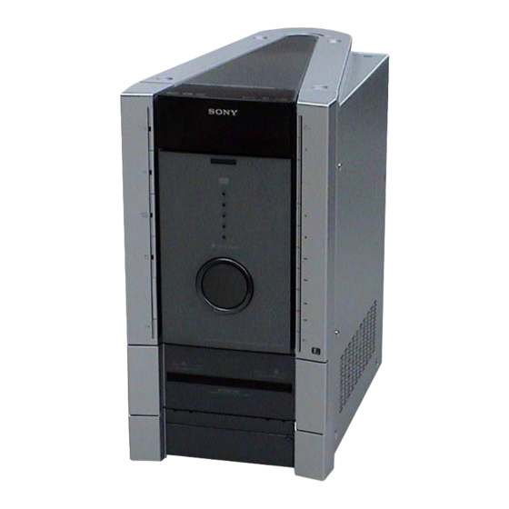
HCD-FLX9W is the amplifier, DVD player, tape deck and
tuner section in DHC-FLX9W.
TE
L 13942296513
Amplifier section:
The following measured at AC 127, 220, 240 V,
50/60 Hz (Saudi Arabian model only)
The following measured at AC 120, 220, 240 V,
50/60 Hz (except for Saudi Arabian model)
MULTI mode
DIN power output at stereo mode (rated)
Continuous RMS power output (reference)
Front speaker:
Center speaker:
Rear speaker:
Sub woofer:
2.1CH mode
DIN power output at stereo mode (rated)
Continuous RMS power output (reference)
www
.
Sony Corporation
9-877-904-01
Home Audio Company
2004G05-1
Published by Sony Engineering Corporation
© 2004.07
http://www.xiaoyu163.com
Front speaker:
Sub woofer:
Inputs
VIDEO/SAT IN L/R (phono jacks):
45 + 45 watts
(8 ohms at 1 kHz, DIN)
OPTICAL DIGITAL IN (Square optical connector
jacks, rear panel) :
60 + 60 watts
wavelength
(8 ohms at 1 kHz, 10%
MIC (phone jack) :
THD)
60 watts
Outputs
(16 ohms at 1 kHz, 10%
VIDEO OUT L/R (phono jacks):
THD)
60 + 60 watts
(6 ohms at 1 kHz, 10%
VIDEO OUT:
THD)
S VIDEO OUT:
100 watts
(8 ohms at 100 Hz, 10%
COMPONENT VIDEO OUT:
THD)
70 + 70 watts
(8 ohms at 1 kHz, DIN)
x
ao
u163
y
i
http://www.xiaoyu163.com
HCD-FLX9W
2 9
8
Model Name Using Similar Mechanism
DVD Mechanism Type
DVD
Section
Base Unit Name
Optical Traverse Unit Name
TAPE
Model Name Using Similar Mechanism
Q Q
Section
3
6 7
1 3
1 5
SPECIFICATIONS
120 + 120 watts
(8 ohms at 1 kHz, 10%
THD)
240 watts
(8 ohms at 100 Hz, 10%
THD)
voltage 250 mV/450 mV,
impedance 47 kilohms
−−−−
sensitivity 1 mV,
impedance 10 kilohms
voltage 250 mV,
impedance 1 kilohms
1 Vp-p, 75 ohms
Y: 1 Vp-p, 75 ohms
C: 0.286 Vp-p, 75 ohms
Y: 1 Vp-p, 75 ohms
P
: 0.7 Vp-p, 75 ohms
B
P
: 0.7 Vp-p, 75 ohms
R
co
.
9 4
2 8
E Model
HCD-FLX5D
CDM53N-DVBU14
DVBU14
DBU-1
HCD-FLX5D
0 5
8
2 9
9 4
2 8
PHONES (stereo mini jack):
accepts headphones of
8 ohms or more
FRONT L/R:
Use only the supplied
speaker SS-FLX9
REAR L/R:
Use only the supplied
speaker SS-RS99
CENTER:
Use only the supplied
speaker SS-CT99
S.WOOFER:
Use only the supplied
speaker SS-WG9
Disc player section
Laser
Semiconductor laser
(DVD and SA-CD:
λ=650 nm,
CD: λ=780 nm)
Emission duration:
continuous
Frequency response
DVD (PCM 48 kHz):
2 Hz − 22 kHz = (±1 dB)
CD: 2 Hz − 20 kHz =
(±1 dB)
– Continued on next page –
m
DVD DECK RECEIVER
9 9
9 9
Advertisement
Table of Contents

Related Manuals for Sony HD-FLX9W


Summary of Contents for Sony HD-FLX9W
-
Page 1: Service Manual
70 + 70 watts – Continued on next page – (8 ohms at 1 kHz, DIN) Continuous RMS power output (reference) DVD DECK RECEIVER u163 Sony Corporation 9-877-904-01 Home Audio Company 2004G05-1 Published by Sony Engineering Corporation © 2004.07 http://www.xiaoyu163.com... - Page 2 COMPONENTS IDENTIFIED BY MARK 0 OR DOTTED LINE WITH MARK 0 ON THE SCHEMATIC DIAGRAMS AND IN THE PARTS LIST ARE CRITICAL TO SAFE OPERATION. REPLACE THESE COMPONENTS WITH SONY PARTS WHOSE PART NUMBERS APPEAR AS SHOWN IN THIS MANUAL OR IN SUPPLEMENTS PUBLISHED BY SONY.
- Page 3 http://www.xiaoyu163.com HCD-FLX9W 3 7 63 1515 0 Depending on the DVD, no region code This system can play the indication may be labeled even though playing the DVD is prohibited by area restrictions. following discs The region code is located below the COMPONENT VIDEO OUT jacks on the rear panel.
-
Page 4: Table Of Contents
http://www.xiaoyu163.com HCD-FLX9W 3 7 63 1515 0 TABLE OF CONTENTS SERVICING NOTES 8-17. Schematic Diagram – MB Board (6/7) – ......53 ..........5 8-18. Schematic Diagram – MB Board (7/7) – ......54 8-19. Schematic Diagram – DSP Board (1/3) – ...... 55 GENERAL 8-20. -
Page 5: Servicing Notes
http://www.xiaoyu163.com HCD-FLX9W SECTION 1 SERVICING NOTES 3 7 63 1515 0 • MODEL IDENTIFICATION NOTES ON HANDLING THE OPTICAL PICK-UP – Back Panel – BLOCK OR BASE UNIT The laser diode in the optical pick-up block may suffer electrostatic break-down because of the potential difference generated by the charged electrostatic load, etc. - Page 6 http://www.xiaoyu163.com HCD-FLX9W 3 7 63 1515 0 DVD MECHANISM DECK SERVICE POSITION • In checking the DVD mechanism deck section (CDM53N-DVBU14), prepare extension jig (Part No. J-2501-103-A: 1.00 mm Pitch, 29 cores, Length 300 mm). DVD mechanism deck (CDM53N-DVBV14) Any board to put. L 13942296513 Connect extension jig (J-2501-103 A) to the MB board (CN501) and...
- Page 7 http://www.xiaoyu163.com HCD-FLX9W 3 7 63 1515 0 DSP/GC/MB/MC/REGULATOR AND VIDEO BOARDS SERVICE POSITION • In checking the DSP/GC/MB/MC/REGULATOR and VIDEO boards, prepare extension jig (Part No. J-2501-103-A: 1.00 mm Pitch, 29 cores, Length 300 mm). DSP board VIDEO board MB board REGULATOR board (CN501) GC board...
- Page 8 http://www.xiaoyu163.com HCD-FLX9W 3 7 63 1515 0 IC501 SERVICE POSITION • When you check IC501, please move a power trans former (T911) from a chassis. IC501 chassis power transformer (T911) DECISION TO PASS OR FAIL OF THE OPTICAL Checking Location: –...
-
Page 9: General
http://www.xiaoyu163.com HCD-FLX9W SECTION 2 This section is extracted from instruction manual. GENERAL 3 7 63 1515 0 Main unit ALPHABETICAL ORDER BUTTON DESCRIPTIONS ?/1 (power) 1 MIC jack ws Z (open/close) 4 CD SYNC HI-DUB qg MIC LEVEL wd A Z (deck A) wh Deck A wg MULTI CHANNEL DECODING Z B (deck B) 0... -
Page 10: Remote Control
DVD SETUP* 9 SHIFT qd x (stop) wl DVD TOP MENU qg SLEEP wg . (go back) wj EFFECT* es SONY TV DIRECT qj > (go forward) wj ENTER 6 SUBTITLE ea m (rewind) ra M (fast forward) ra V/v/B/b/ENTER eg >10 wa... -
Page 11: Disassembly
http://www.xiaoyu163.com HCD-FLX9W SECTION 3 DISASSEMBLY 3 7 63 1515 0 • This set can be disassembled in the order shown below. 3-1. DISASSEMBLY FLOW 3-2. COVER (TOP), COVER (BACK) (Page 12) 3-3. CASE (Page 12) 3-4. FRONT PANEL ASSY (Page 13) 3-5. -
Page 12: Cover (Top), Cover (Back)
http://www.xiaoyu163.com HCD-FLX9W 3 7 63 1515 0 Note: Follow the disassembly procedure in the numerical order given. 3-2. COVER (TOP), COVER (BACK) 1 four screws 4 two claws (case 3 TP2) 2 cover (top) 3 two screws (BVTP3 × 8) 5 cover (back) 3 three screws (BVTP3 ×... -
Page 13: Front Panel Assy
http://www.xiaoyu163.com HCD-FLX9W 3 7 63 1515 0 3-4. FRONT PANEL ASSY 3 two connectors (CN203, CN208) 2 wire (flat type) (17 core) (CN206) 3 connector 3 connector (CN207) (CN201) MC board 1 wire (flat type) (17 core) (CN109) L 13942296513 6 connector (NO803) 6 three connectors... -
Page 14: Mechanical (Cassette) Deck
http://www.xiaoyu163.com HCD-FLX9W 3 7 63 1515 0 3-5. MECHANICAL (CASSETTE) DECK 4 Push two plunger solenoids 1 two screws (BVTP2.6 × 8) 2 cover (TC) 6 mechanical (cassette) deck 5 Open the lid (TC) 3 two screws (BVTP2.6 × 3) L 13942296513 3-6. -
Page 15: Dvd Mechanism Block
http://www.xiaoyu163.com HCD-FLX9W 3 7 63 1515 0 3-7. DVD MECHANISM BLOCK MC board 2 connector 2 two connectors 3 six screws (CN807) (CN702, CN703) (BVTP3 × 8) SP RELAY board 5 two claws 4 two connectors (CN805, CN806) 6 claw 2 two connectors 7 DVD mechanism block (CN0005, CN7002) -
Page 16: Dvd Mechanism Deck (Cdm53N-Dvbu14)
http://www.xiaoyu163.com HCD-FLX9W 3 7 63 1515 0 3-9. DVD MECHANISM DECK (CDM53N-DVBU14) 3 wire (flat type) (29core) Note: Please turn a DSP/MB/MC boards side down (CN501) and do not do decomposition work. DVD mechanism deck (CDM53N-DVBU14) 1 two screws (BVTP3 × 8) 2 bracket (FL) 4 four screws... -
Page 17: Base Unit (Dvbu14)
http://www.xiaoyu163.com HCD-FLX9W 3 7 63 1515 0 3-11. BASE UNIT (DVBU14) 2 four screws (BTTP M2.6) 4 magnet assy 1 connector (CN710) 5 two screws 3 two hooks 6 base unit (PTPWH M2.6) (DVBU14) L 13942296513 3-12. TRAY (SUB) 1 Rotating the pulley (LD), shift the slider (selection) in the arrow A direction. 2 Rotating the pulley (mode) in the arrow direction, adjust the tray (sub) to be removed. -
Page 18: Chassis (Mold B) Section, Stocker Section, Slider (Selection)
http://www.xiaoyu163.com HCD-FLX9W 3 7 63 1515 0 3-13. CHASSIS (MOLD B) SECTION, STOCKER SECTION, SLIDER (SELECTION) 7 two screws (PTPWH M2.6) 6 stocker section 8 slider (selection) 9 washer 0 compression 1 three screws spring (BVTP M2.6) pully (LD) 5 two step screws 2 chassis (mold B) section Note: Rotating the pully (LD),... -
Page 19: Sub Trans Board
http://www.xiaoyu163.com HCD-FLX9W 3 7 63 1515 0 3-15. SUB TRANS BOARD 1 connector (CN901) 2 three screws (BVTP3 × 8) 1 connector (CN902) 4 ground terminal 5 SUB TRANS board L 13942296513 3-16. BACK PANEL SECTION 2 two screws (BVTP3 × 8) 1 connector (CN902) 4 connector... -
Page 20: Trans Board
http://www.xiaoyu163.com HCD-FLX9W 3 7 63 1515 0 3-17. TRANS BOARD 2 four screws 1 connector (CN914) 3 TRANS board 1 connector (CN915) 1 connector (CN916) L 13942296513 3-18. SP RELAY BOARD 5 connector (CN801) 3 two connectors (CN803, CN804) 6 SP RELAY board 4 PC board holder FRONT REAR AMP board 1 two screws... -
Page 21: Assembly 4-1. Assembly Flow
http://www.xiaoyu163.com HCD-FLX9W SECTION 4 ASSEMBLY 3 7 63 1515 0 • This set can be assembled in the order shown below. 4-1. ASSEMBLY FLOW 4-2. GEARS INSTALLATION (Page 21) 4-3. SLIDER (SELECTION) INSTALLATION (Page 22) 4-4. STOCKER SECTION INSTALLATION (Page 22) 4-5. -
Page 22: Slider (Selection) Installation
http://www.xiaoyu163.com HCD-FLX9W 3 7 63 1515 0 4-3. SLIDER (SELECTION) INSTALLATION 6 two screws (PTPWH M2.6) 2 gear (chuking) rotary encoder 5 washer 4 compression spring 7 Insert the slider (selection) into the portion A. Align with the slot of rotary encoder. -
Page 23: Chassis (Mold B) Section Installation
http://www.xiaoyu163.com HCD-FLX9W 3 7 63 1515 0 4-5. CHASSIS (MOLD B) SECTION INSTALLATION 3 three screws (BVTP M2.6) 2 Insert the gear (eject) 1 Insert the portion A of under the gear (LD chassis (mold B) section deceleration). portion A into the portion B of slider (selection). -
Page 24: Test Mode
http://www.xiaoyu163.com HCD-DFLX9W SECTION 5 3 7 63 1515 0 TEST MODE [COLD RESET] Each time the “CASSETTE LID OPEN/CLOSE DETECT” • The cold reset clears all data including preset data stored in switch is pressed, “T” value increases. 8. Also when [GROOVE] is pressed after lighting of all LEDs the RAM to initial conditions. - Page 25 http://www.xiaoyu163.com HCD-DFLX9W 3 7 63 1515 0 Volume check: [DVD SHIP MODE (NO MEMORY CLEAR) ] • This mode moves the optical pick-up to the position durable 1. When the [VOLUME] knob is turned clockwise even slightly, the sound volume increases to its maximum and a message to vibration.
- Page 26 http://www.xiaoyu163.com HCD-DFLX9W 3 7 63 1515 0 [DVD TEST MODE GENERAL DESCRIPTION] 0-1. All (All items continuous check) This menu checks all diagnostic items continuously. Normally, all The Test Mode allows you to make diagnosis and adjustment easily items are checked successively one after another automatically using the remote commander and monitor TV.
- Page 27 http://www.xiaoyu163.com HCD-DFLX9W 3 7 63 1515 0 0-2. Version 1. DRIVE AUTO ADJUSTMENT 0-2-2. Revision On the Test Mode Menu screen, press the [1] key on the remote The revision number of ROM (IC204) that the program for commander, and the Adjustment Menu will be displayed. the DVD system processor (IC206) is stored.
- Page 28 http://www.xiaoyu163.com HCD-DFLX9W 3 7 63 1515 0 2. DRIVE MANUAL OPERATION 2-1. Disc Type Note: This mode is used for design, and not used in service fundamentally. Disc Type On the Test Mode Menu screen, press the [2] key on the remote commander, and the Operation Menu will be displayed.
- Page 29 http://www.xiaoyu163.com HCD-DFLX9W 3 7 63 1515 0 2-1-3. Disc Type CD 2-3. Track/Layer Jump It sets up so that it may judge as a disc type of specification of the disc with which the set was inserted. Track/Layer Jump [1]: CD disc (normal speed, 12 cm) FWD R.Lj L0>L1 [2]: CD disc (double speed, 12 cm) REV L.Lj L1>L0...
- Page 30 http://www.xiaoyu163.com HCD-DFLX9W 3 7 63 1515 0 2-5. EEPROM Write Adjust 2-7. Disc Check Memory EEPROM Write Adjust Disc Check Memory 1. Focus Offset 1. SL Disc check 2. Focus Gain 2. CD Disc check 3. Trk. Offset Coarse 3. DL Disc check 4.
- Page 31 http://www.xiaoyu163.com HCD-DFLX9W 3 7 63 1515 0 • Code list of Emergency History 3. MECHA AGING 10: Communication to RF AMP (IC001) failed. On the Test Mode Menu screen, selecting [3] executes the aging of 11: Each servo for focus, tracking, and spindle is unlocked. the mechanism deck.
- Page 32 http://www.xiaoyu163.com HCD-DFLX9W 3 7 63 1515 0 • Error code (aa) 6. VERSION INFORMATION FF : Complete the initializing. (normal operation) On the Test Mode Menu screen, selecting [6] displays the ROM 11 : Stocker movement (to chucking position) failing in the midst version and region code.
-
Page 33: Mechanical Adjustments
http://www.xiaoyu163.com HCD-DFLX9W SECTION 7 SECTION 6 ELECTRICAL ADJUSTMENTS 3 7 63 1515 0 MECHANICAL ADJUSTMENTS Precaution DECK SECTION 0 dB=0.775 V 1. Clean the following parts with a denatured alcohol-moistened swab: 1. Demagnetize the record/playback head with a head record/playback heads pinch rollers demagnetizer. - Page 34 http://www.xiaoyu163.com HCD-DFLX9W 3 7 63 1515 0 3. Mode: Playback 1. Insert the WS-48B into the deck B. 2. Press the button on the deck B. test tape 3. Press the [CD SYNC HI-DUB] button in playback mode. P-4-A100 oscilloscope Then at HIGH speed mode.
-
Page 35: Dvd Section
http://www.xiaoyu163.com HCD-FLX9W 3 7 6 3 1 5 1 5 0 Adjustment Location: REC LEVEL ADJUSTMENT DECK B DVD SECTION – TX Board (Component Side) – About the dicision to pass or fail of the optical pick-up block, refer Procedure: to “DICISION TO PASS OR FAIL OF THE OPTICAL PICK-UP In the MC test mode, the “REC memory mode”... -
Page 36: Diagrams
http://www.xiaoyu163.com HCD-FLX9W SECTION 8 3 7 6 3 1 5 1 5 0 DIAGRAMS 8-1. BLOCK DIAGRAM – RF SERVO Section – • SIGNAL PATH WARFI (Page 38) : AUDIO : CD PLAY CDDOUT (Page 39) : DVD PLAY : VIDEO : SACD PLAY 117 RFIN SD0 –... -
Page 37: Block Diagram - Tuner/Tape Deck Section
http://www.xiaoyu163.com HCD-FLX9W 3 7 6 3 1 5 1 5 0 8-2. BLOCK DIAGRAM – TUNER/TAPE DECK Section – FM/AM TUNER PACK TUNER FM 75Ω L-CH (Page 39) FM ANT L-CH COAXIAL R-CH R-CH ANT GND ANTENNA ST-DOUT AM ANT ST-DIN ST-CLK ANT GND... -
Page 38: Block Diagram - Audio Dsp Section (1/2)
http://www.xiaoyu163.com HCD-FLX9W 3 7 6 3 1 5 1 5 0 8-3. BLOCK DIAGRAM – AUDIO DSP Section (1/2) – WARFI RF BUFFER (Page 36) 39 DSIFL 126 WARFI DSAL FLR, CSW, SLR, IC810 MCK, BCK, LRCK DSAR 40 DSIFR (Page 36) 123 WCK (Page 39) -
Page 39: Block Diagram - Audio Dsp Section (2/2)
http://www.xiaoyu163.com HCD-FLX9W 3 7 6 3 1 5 1 5 0 8-4. BLOCK DIAGRAM – AUDIO DSP Section (2/2) – TUNER L-CH • R-ch is omitted due to same as L-ch. (Page 37) • SIGNAL PATH TAPE J701 (1/2) L-CH : AUDIO : TAPE PLAY : REC... -
Page 40: Block Diagram - Power Amp Section
http://www.xiaoyu163.com HCD-FLX9W 3 7 6 3 1 5 1 5 0 8-5. BLOCK DIAGRAM – POWER AMP Section – J301 HP SW (Page 42) TM801 –2 FEED BACK (Page 39) FRONT L –2 – –1 –1 FRONT R (Page 39) –... -
Page 41: Block Diagram - Video Section
http://www.xiaoyu163.com HCD-FLX9W 3 7 6 3 1 5 1 5 0 8-6. BLOCK DIAGRAM – VIDEO Section – • SIGNAL PATH : VIDEO VDAC_0 : CHROMA SD0 – SD7 (Page 36) AV DATA BUS VIDEO AMP, 75Ω DRIVER : COMPONENT VIDEO IC701 VDAC_2 6 YIN... -
Page 42: Block Diagram - Display/Power Supply Section
http://www.xiaoyu163.com HCD-FLX9W 8-7. BLOCK DIAGRAM – DISPLAY/POWER SUPPLY Section – CD/DVD DOOR OPEN/CLOSE 3 7 6 3 1 5 1 5 0 MOTOR DRIVE IC302 EVER+4V S702 (LID) PRTC_SW OUT1 M301 DOOR MOTOR+ (ON: When CD/DVD lid is close.) MOTOR D103, 104 CD/DVD DOOR OUT2... - Page 43 http://www.xiaoyu163.com HCD-FLX9W 3 7 6 3 1 5 1 5 0 • Note for Printed Wiring Boards and Schematic Diagrams • Circuit Boards Location Note on Printed Wiring Board: Note on Schematic Diagram: • X : parts extracted from the component side. FRONT REAR AMP board •...
-
Page 44: Printed Wiring Board - Rf Board
http://www.xiaoyu163.com HCD-FLX9W 3 7 6 3 1 5 1 5 0 • See page 43 for Circuit Boards Location. 8-8. PRINTED WIRING BOARD – RF Board – :Uses unleaded solder. RF BOARD RF BOARD (COMPONENT SIDE) (CONDUCTOR SIDE) R041 C003 C001 Q002 R009... -
Page 45: Schematic Diagram - Rf Board
http://www.xiaoyu163.com HCD-FLX9W 3 7 6 3 1 5 1 5 0 • See page 92 for IC Block Diagram. • See page 90 for Waveforms. 8-9. SCHEMATIC DIAGRAM – RF Board – RFMON C006 C028 C027 R026 C013 CN002 C030 0.01 C026 AGND... -
Page 46: Mb Board (Component Side)
http://www.xiaoyu163.com HCD-FLX9W • See page 43 for Circuit Boards Location. 8-10. PRINTED WIRING BOARD – MB Board (Component Side) – : Uses unleaded solder. 3 7 6 3 1 5 1 5 0 • Semiconductor Location Ref. No. Location DSP BOARD D201 B-10 CN603... -
Page 47: Mb Board (Conductor Side)
http://www.xiaoyu163.com HCD-FLX9W • See page 43 for Circuit Boards Location. : Uses unleaded solder. 8-11. PRINTED WIRING BOARD – MB Board (Conductor Side) – 3 7 6 3 1 5 1 5 0 • Semiconductor Location Ref. No. Location D901 MB BOARD (CONDUCTOR SIDE) IC202... -
Page 48: Schematic Diagram - Mb Board (1/7)
http://www.xiaoyu163.com HCD-FLX9W 3 7 6 3 1 5 1 5 0 • See page 92 for IC Block Diagram. • See page 90 for Waveforms. • See page 100 for IC Pin Function Description. 8-12. SCHEMATIC DIAGRAM – MB Board (1/7) – (1/7) AGND A3V-1... -
Page 49: Schematic Diagram - Mb Board (2/7)
http://www.xiaoyu163.com HCD-FLX9W • See page 90 for Waveforms. • See page 100 for IC Pin Function Description. 8-13. SCHEMATIC DIAGRAM – MB Board (2/7) – 3 7 6 3 1 5 1 5 0 (2/7) JITOFF RF_AC TP701 R726 100k R700 R725 C721... -
Page 50: Schematic Diagram - Mb Board (3/7)
http://www.xiaoyu163.com HCD-FLX9W 3 7 6 3 1 5 1 5 0 • See page 92 for IC Block Diagrams. • See page 90 for Waveforms. • See page 100 for IC Pin Function Description. 8-14. SCHEMATIC DIAGRAM – MB Board (3/7) – (3/7) DGND C795... -
Page 51: Schematic Diagram - Mb Board (4/7)
http://www.xiaoyu163.com HCD-FLX9W 3 7 6 3 1 5 1 5 0 • See page 92 for IC Block Diagrams. • See page 90 for Waveforms. • See page 100 for IC Pin Function Description. 8-15. SCHEMATIC DIAGRAM – MB Board (4/7) – (Page 49) (4/7) 768FS... -
Page 52: Schematic Diagram - Mb Board (5/7)
http://www.xiaoyu163.com HCD-FLX9W • See page 90 for Waveforms. • See page 100 for IC Pin Function Description. 8-16. SCHEMATIC DIAGRAM – MB Board (5/7) – 3 7 6 3 1 5 1 5 0 (5/7) CN204 R258 R259 R257 C228 4.7k 4.7k 4.7k... -
Page 53: Schematic Diagram - Mb Board (6/7)
http://www.xiaoyu163.com HCD-FLX9W 3 7 6 3 1 5 1 5 0 • See page 92 for IC Block Diagram. 8-17. SCHEMATIC DIAGRAM – MB Board (6/7) – (6/7) MD15 FL202 FL203 C217 C257 C258 0.01 0.01 MD14 C219 C253 0.01 0.01 MD13 R249... -
Page 54: Schematic Diagram - Mb Board (7/7)
http://www.xiaoyu163.com HCD-FLX9W • See page 92 for IC Block Diagram. 8-18. SCHEMATIC DIAGRAM – MB Board (7/7) – 3 7 6 3 1 5 1 5 0 (7/7) BUFFER IC402 SN74LV245APWR C411 0.01 CN401 LRCK R431 R432 LRCK R433 R434 256FS R435 R429... -
Page 55: Schematic Diagram - Dsp Board (1/3)
http://www.xiaoyu163.com HCD-FLX9W 3 7 6 3 1 5 1 5 0 • See page 90 for Waveforms. • See page 100 for IC Pin Function Description. 8-19. SCHEMATIC DIAGRAM – DSP Board (1/3) – (1/3) CN602 JR617 SPDIF(DVD) D+4V SPDIF(CD) JR616 D-GND(DSP) (Page 56) -
Page 56: Schematic Diagram - Dsp Board (2/3)
http://www.xiaoyu163.com HCD-FLX9W 3 7 6 3 1 5 1 5 0 8-20. SCHEMATIC DIAGRAM – DSP Board (2/3) – J701 VIDEO/SAT (CHASSIS GND) (2/3) (EA) FB702 C794 220p R703 R753 D751 D750 RB501V RB501V C741 R701 C704 C754 220p 220p R754 (EA) (EXCEPT EA) -
Page 57: Schematic Diagram - Dsp Board (3/3)
http://www.xiaoyu163.com HCD-FLX9W • See page 92 for IC Block Diagrams. • See page 90 for Waveforms. 8-21. SCHEMATIC DIAGRAM – DSP Board (3/3) – 3 7 6 3 1 5 1 5 0 (Page 56) (3/3) R657 1.5k JR623 R656 R654 (EA) C662... -
Page 58: Printed Wiring Board - Dsp Board (Component Side)
http://www.xiaoyu163.com HCD-FLX9W 3 7 6 3 1 5 1 5 0 • See page 43 for Circuit Boards Location. 8-22. PRINTED WIRING BOARD – DSP Board (Component Side) – : Uses unleaded solder. DSP BOARD (COMPONENT SIDE) R635 R637 C641 X602 R636 R641... -
Page 59: Printed Wiring Board - Dsp Board (Conductor Side)
http://www.xiaoyu163.com HCD-FLX9W 3 7 6 3 1 5 1 5 0 • See page 43 for Circuit Boards Location. 8-23. PRINTED WIRING BOARD – DSP Board (Conductor Side) – : Uses unleaded solder. I/F BOARD CN0004 (Page 60) MB BOARD CN401 (Page 46) DSP BOARD... -
Page 60: Printed Wiring Boards - Diat Section
http://www.xiaoyu163.com HCD-FLX9W • See page 43 for Circuit Boards Location. :Uses unleaded solder. 8-24. PRINTED WIRING BOARDS – DIAT Section – 3 7 6 3 1 5 1 5 0 • Semiconductor Location Ref. No. Location I/F BOARD TX OUT BOARD D004 D0001 CN0003... -
Page 61: Schematic Diagram - Diat Section
http://www.xiaoyu163.com HCD-FLX9W 3 7 6 3 1 5 1 5 0 8-25. SCHEMATIC DIAGRAM – DIAT Section – D0006 EP0002 1SS133T D0005 1SS133T (CHASSIS) C0008 220p CN0004 CN0007 (Page 55) LRCK D0007 1SS133T DATA D0008 1SS133T CN0005 C0006 220p 3.3V SCLK (Page 63) CN0006... -
Page 62: Printed Wiring Board - Tx Board
http://www.xiaoyu163.com HCD-FLX9W 3 7 6 3 1 5 1 5 0 • See page 43 for Circuit Boards Location. 8-26. PRINTED WIRING BOARD – TX Board – : Uses unleaded solder. • Semiconductor Location Ref. No. Location I/F BOARD D7001 CN0007 D7002 (Page 60) -
Page 63: Schematic Diagram - Tx Board
http://www.xiaoyu163.com HCD-FLX9W 3 7 6 3 1 5 1 5 0 • See page 92 for IC Block Diagrams. • See page 90 for Waveform. 8-27. SCHEMATIC DIAGRAM – TX Board – L7001 10µH C7001 C7002 L7002 L7003 L7004 10µH 10µH 10µH R7001... -
Page 64: Printed Wiring Board - Mc Board
http://www.xiaoyu163.com HCD-FLX9W 3 7 6 3 1 5 1 5 0 8-28. PRINTED WIRING BOARD – MC Board – • See page 43 for Circuit Boards Location. : Uses unleaded solder. • Semiconductor Location ANTENNA Ref. No. Location FM 75Ω D101 COAXIAL D102... -
Page 65: Schematic Diagram - Mc Board
http://www.xiaoyu163.com HCD-FLX9W 3 7 6 3 1 5 1 5 0 • See page 90 for Waveforms. • See page 100 for IC Pin Function Description. 8-29. SCHEMATIC DIAGRAM – MC Board – (Page 51) CN112 *SUPPLIED WITH R272 R273 THE ASSEMBLED CN105 BLOCK... -
Page 66: Printed Wiring Board - Front Rear Amp Board
http://www.xiaoyu163.com HCD-FLX9W 3 7 6 3 1 5 1 5 0 8-30. PRINTED WIRING BOARD – FRONT REAR AMP Board – • See page 43 for Circuit Boards Location. :Uses unleaded solder. SP RELAY BOARD CN801 (Page 70) FRONT REAR AMP BOARD CN402 JW402 JW403... -
Page 67: Schematic Diagram - Front Rear Amp Board
http://www.xiaoyu163.com HCD-FLX9W 8-31. SCHEMATIC DIAGRAM – FRONT REAR AMP Board – 3 7 6 3 1 5 1 5 0 POWER AMP IC401 STK402-070S R455 NO701 0.22 C455 C456 R460 AC1(VL) AC1(VL) AC-GND R457 R456 0.22 AC-GND D491 D15XB20 AC1(VL) AC1(VL) R454 (Page 87) -
Page 68: Printed Wiring Board - Center Sw Amp Board
http://www.xiaoyu163.com HCD-FLX9W 8-32. PRINTED WIRING BOARD – CENTER SW AMP Board – • See page 43 for Circuit Boards Location. 3 7 6 3 1 5 1 5 0 : Uses unleaded solder. • Semiconductor Location Ref. No. Location TRANS BOARD (Page 86) CN916 CENTER SW AMP BOARD... -
Page 69: Schematic Diagram - Center Sw Amp Board
http://www.xiaoyu163.com HCD-FLX9W 3 7 6 3 1 5 1 5 0 8-33. SCHEMATIC DIAGRAM – CENTER SW AMP Board – NO702 AC2(VH) AC2(VH) AC GND POWER AMP AC GND IC501 STK442-130 AC2(VH) AC2(VH) AC3(MOTOR) D591 (Page 87) RECT D591 D15XB20 AC3(MOTOR) C593 C591... -
Page 70: Printed Wiring Boards - Speaker Section
http://www.xiaoyu163.com HCD-FLX9W 8-34. PRINTED WIRING BOARDS – SPEAKER Section – 3 7 6 3 1 5 1 5 0 • See page 43 for Circuit Boards Location. : Uses unleaded solder. • Semiconductor Location REGULATOR BOARD Ref. No. Location C878 C871 C872 C880... -
Page 71: Schematic Diagram - Regulator Board
http://www.xiaoyu163.com HCD-FLX9W 3 7 6 3 1 5 1 5 0 8-35. SCHEMATIC DIAGRAM – REGULATOR Board – IC801 TA7804LS C870 C878 +4V REGULATOR IC802 TA7805S C871 C879 NO704 +5V REGULATOR IC803 TA7810S C872 C880 +10V REGULATOR IC804 (Page 73) TA7805S C873 C881... -
Page 72: Schematic Diagram - Sp Relay Board (1/2)
http://www.xiaoyu163.com HCD-FLX9W 3 7 6 3 1 5 1 5 0 • See page 92 for IC Block Diagram. • See page 90 for Waveforms. 8-36. SCHEMATIC DIAGRAM – SP RELAY Board (1/2) – (1/2) DVD+12V CD/DVD POWER M-GND M+9V UNREG-GND NO816 UNREG(M) -
Page 73: Schematic Diagram - Sp Relay Board (2/2)
http://www.xiaoyu163.com HCD-FLX9W 3 7 6 3 1 5 1 5 0 8-37. SCHEMATIC DIAGRAM – SP RELAY Board (2/2) – (Page 67) (Page 87) CN803 OVERLOAD STK MUTE POWER GND POWER GND CN801 NO703 CENTER GND CENTER GND R815 C815 CENTER (2/2) 100V... -
Page 74: Printed Wiring Board - Gc Board
http://www.xiaoyu163.com HCD-FLX9W 8-38. PRINTED WIRING BOARD – GC Board – 3 7 6 3 1 5 1 5 0 • See page 43 for Circuit Boards Location. : Uses unleaded solder. • Semiconductor Location Ref. No. Location D201 GC BOARD D202 D203 D204... -
Page 75: Schematic Diagram - Gc Board
http://www.xiaoyu163.com HCD-FLX9W • See page 90 for Waveform. • See page 100 for IC Pin Function Description. 8-39. SCHEMATIC DIAGRAM – GC Board – 3 7 6 3 1 5 1 5 0 FL201 FLUORESCENT INDICATOR TUBE EP202 C209 C221 (CHASSIS) CN201 EVER+3.3V... -
Page 76: Printed Wiring Boards - Changer Section
http://www.xiaoyu163.com HCD-FLX9W 8-40. PRINTED WIRING BOARDS – CHANGER Section – 3 7 6 3 1 5 1 5 0 • See page 43 for Circuit Boards Location. : Uses unleaded solder. CLAMP MOTOR BOARD INIT/COUNT SW BOARD SENSOR 2 BOARD OUT/MIDOUT SW BOARD S702 (LID) ON : WHEN CD LID... -
Page 77: Q Q 8-41. Schematic Diagram - Changer Section
http://www.xiaoyu163.com HCD-FLX9W • See page 92 for IC Block Diagrams. 8-41. SCHEMATIC DIAGRAM – CHANGER Section – 3 7 6 3 1 5 1 5 0 D704 GL528VS1 CN708 CN702 DISC IN DETECT R711 SENSOR R707 R709 2.2k Q701 RT1N141 R708 LEVEL SHIFT... -
Page 78: Printed Wiring Boards - Cd Door Section
http://www.xiaoyu163.com HCD-FLX9W 3 7 6 3 1 5 1 5 0 8-42. PRINTED WIRING BOARDS – CD DOOR Section – • See page 43 for Circuit Boards Location. : Uses unleaded solder. CD MOTOR BOARD BLUE LED BOARD D308 C316 MULTI CHANNEL DECODING (12) 1-861-348-... -
Page 79: Schematic Diagram - Cd Door Section
http://www.xiaoyu163.com HCD-FLX9W 3 7 6 3 1 5 1 5 0 • See page 92 for IC Block Diagram. 8-43. SCHEMATIC DIAGRAM – CD DOOR Section – NO807B NO807A (Page 75) CN309 R384 4.7k R388 4.7k R383 4.7k R387 4.7k D308 S341 SELU5E23C... -
Page 80: Printed Wiring Boards - Panel Section
http://www.xiaoyu163.com HCD-FLX9W 3 7 6 3 1 5 1 5 0 • See page 43 for Circuit Boards Location. 8-44. PRINTED WIRING BOARDS – PANEL Section – :Uses unleaded solder. PANEL (L) BOARD R307 D304 D303 D302 D301 R338 R308 R309 R303 D304, S307... -
Page 81: Schematic Diagram - Panel Section
http://www.xiaoyu163.com HCD-FLX9W 3 7 6 3 1 5 1 5 0 8-45. SCHEMATIC DIAGRAM – PANEL Section – R302 R321 R322 R323 R324 R325 R326 R327 R328 1.5k 1.5k 2.2k 3.3k 4.7k 6.8k S311 S312 S313 S314 S315 S316 S317 S318 S319 D304... -
Page 82: Printed Wiring Board - Mic Board
http://www.xiaoyu163.com HCD-FLX9W 3 7 6 3 1 5 1 5 0 • See page 43 for Circuit Boards Location. 8-46. PRINTED WIRING BOARD – MIC Board – :Uses unleaded solder. MIC BOARD C380 C368 C373 R366 IC352 RV352 R370 ECHO LEVEL R375 R371 C372... -
Page 83: Schematic Diagram - Mic Board
http://www.xiaoyu163.com HCD-FLX9W 3 7 6 3 1 5 1 5 0 • See page 92 for IC Block Diagram. 8-47. SCHEMATIC DIAGRAM – MIC Board – C360 R358 100p 150k MIC AMP IC351(2/2) C358 IC351(1/2) C351 C361 C356 NJM4580E-D R357 NJM4580E-D R352 0.22... -
Page 84: Printed Wiring Board - Video Board
http://www.xiaoyu163.com HCD-FLX9W 3 7 6 3 1 5 1 5 0 • See page 43 for Circuit Boards Location. 8-48. PRINTED WIRING BOARDS – VIDEO Board – :Uses unleaded solder. MB BOARD CN204 (Page 46) VIDEO BOARD CN701 L701 JW710 C765 C764 C766... -
Page 85: Schematic Diagram - Video Board
http://www.xiaoyu163.com HCD-FLX9W 3 7 6 3 1 5 1 5 0 • See page 92 for IC Block Diagram. • See page 90 for Waveforms. 8-49. SCHEMATIC DIAGRAM – VIDEO Board – CN701 VIDEO AMP, 75Ω DRIVER VGND IC701 J701 VMUTE1 MM1568 R722... -
Page 86: Printed Wiring Board - Trans Board
http://www.xiaoyu163.com HCD-FLX9W 3 7 6 3 1 5 1 5 0 • See page 43 for Circuit Boards Location. 8-50. PRINTED WIRING BOARD – TRANS Board – :Uses unleaded solder. TRANS BOARD R912 Q971 R914 D912 R917 D914 R916 (EXCEPT TH) R915 SP RELAY BOARD... -
Page 87: Schematic Diagram - Trans Board
http://www.xiaoyu163.com HCD-FLX9W 3 7 6 3 1 5 1 5 0 8-51. SCHEMATIC DIAGRAM – TRANS Board – CN915 AC1(VL) AC1(VL) AC GND AC GND AC1(VL) AC1(VL) (Page 67) (TH) (EXCEPT TH) T911 (EXCEPT TH) MAIN F916 (TH) T8AL POWER 250V TRANSFORMER JW922... -
Page 88: Printed Wiring Board - Sub Trans Board
http://www.xiaoyu163.com HCD-FLX9W • See page 43 for Circuit Boards Location. 8-52. PRINTED WIRING BOARDS – SUB TRANS Board – :Uses unleaded solder. 3 7 6 3 1 5 1 5 0 SUB TRANS BOARD (EXCEPT TH) NO606 T901 SUB POWER (CHASSIS) TRANSFORMER S901... -
Page 89: Schematic Diagram - Sub Trans Board
http://www.xiaoyu163.com HCD-FLX9W 3 7 6 3 1 5 1 5 0 8-53. SCHEMATIC DIAGRAM – SUB TRANS Board – * CN902 (TH) (EXCEPT TH) (EXCEPT TH) JW911 (EXCEPT TH) JW912 CN902 F913 (TH) T5AL 250V JW907 (Page 87) JW906 (TH) (EXCEPT TH) R904 (EXCEPT TH) - Page 90 http://www.xiaoyu163.com HCD-FLX9W 3 7 6 3 1 5 1 5 0 • Waveforms – RF Board – – MB Board – IC001 1 (DVDRFP) IC509 q; (WFCK) IC509 ua (XTAI) IC801 qa (MCKI) IC906 3 (MO1) IC206 <zcz (VDAC 0) (CD/DVD PLAY) (CD/DVD PLAY) (CD/DVD PLAY)
- Page 91 http://www.xiaoyu163.com HCD-FLX9W 3 7 6 3 1 5 1 5 0 – DSP Board – – TX Board – – SP RELAY Board – – GC Board – – VIDEO Board – IC601 qs (MCLK2) IC611 qh (SYSCK) IC7002 tl (OSCO) Q4, Q5 (Base) IC201 id (XO) IC701 qk, ql (CR OUT)
- Page 92 http://www.xiaoyu163.com HCD-FLX9W 3 7 6 3 1 5 1 5 0 • IC Block Diagrams – RF Board – – MB Board – IC215 SN74ALVCH16841DGGR IC401 CXD9850Q IC001 SP3723CAF0PM 64 63 62 61 60 59 55 54 53 52 56 1LE FAST ATTACK INPUT OUTPUT...
- Page 93 http://www.xiaoyu163.com HCD-FLX9W 3 7 63 1515 0 IC509 CXD3068Q 59 58 57 56 55 54 53 52 51 50 49 48 47 46 45 44 43 42 41 DVDD2 ASYE DIGITAL ASYMMETRY CORRECTOR DIGITAL DOUT LRCK D/A DIGITAL PCMD INTERFACE DEMODULATOR TES1 TEST1...
- Page 94 http://www.xiaoyu163.com HCD-FLX9W 3 7 63 1515 0 IC706 MSM51V18165F-60TSKR1 40 – 36 34 33 REFRESH INTERNAL TIMING CONTROL ADDRESS GENERATOR CLOCK COUNTER CONTROLLER OUTPUT INPUT BUFFER BUFFER COLUMN CONTROLLER ADDRESS ADDRESS BUFFERS BUFFERS SENSE COLUMN AMPLIFIER DECODERS OUTPUT INPUT BUFFER BUFFER MEMORY WORD...
- Page 95 http://www.xiaoyu163.com HCD-FLX9W 3 7 63 1515 0 IC814 TC7WH157FK (TE85R) IC902 TC7S32FU (TE85R) IN B OUT Y IN A 11 7 11 6 SELECT EN G GND 4 IC903 BR24C08F-E2 IC904 TC7W74FU START STOP LOGIC SERIAL CONTROL H.V. PUMP/TIMING LOGIC LOAD DATA RECOVERY COMP...
- Page 96 http://www.xiaoyu163.com HCD-FLX9W 3 7 63 1515 0 – DSP Board – IC603 LC89057W-VF4-E MODULATOR MICROCONTROLLER & INTERFACE PARALLEL PORT RERR RXOUT CKST AUDIO/VO C bit, U bit EMPHA/UO 31 DGND DATA INPUT DEMODULATOR DVDD SELECTOR DATA & DGND SELECTOR LOCK DETECT DVDD RX5/V1 RX6/U1...
- Page 97 http://www.xiaoyu163.com HCD-FLX9W 3 7 63 1515 0 IC612 PCM1609KPTR 36 35 34 33 VCC3 FUNCTION AGND3 CONTROL VCC4 INTERFACE AGND4 SYSTEM SCKI CLOCK SCKO MANAGER VOUT8 AGND6 VCC5 LRCK AGND5 TEST 4X/8X ENHANCED VOUT7 MULTI- OVER SAMPLING SERIAL DIGITAL LEVEL INPUT FILTER DELTA-...
- Page 98 http://www.xiaoyu163.com HCD-FLX9W 3 7 63 1515 0 IC7002 CXD4016R 48 47 46 45 44 41 40 39 38 37 36 TEST4 TEST3 TEST2 CLOCK TEST1 SELECTOR TEST0 DAVRO READ- LRCK 49 DAVREF AUDIO SOLOMON BUFFER BCK 50 MODULATOR DAAVS INTERFACE PARITY CONVERTER BCKOUT 51...
- Page 99 http://www.xiaoyu163.com HCD-FLX9W 3 7 63 1515 0 – MIC Board – IC352 M65850FP-E1 IC351 NJM4580E-D A OUT B OUT A –IN OSCILLATOR LPF2 A +IN B –IN 1/2 VCC CLOCK B +IN V– AUTO MAIN 20KBIT RESET RESET CONTROL SRAM LPF1 –...
- Page 100 http://www.xiaoyu163.com HCD-FLX9W 3 7 63 1515 0 • IC Pin Function Description MB BOARD IC206 ZIVA5X-C1F (DVD SYSTEM PROCESSOR) Pin No. Pin Name Description VDDP — Power supply terminal (+3.3V) Address signal output to the program ROM and bus interface 3 to 11 HAD15 to HAD7 Two-way data bus with the program ROM and bus interface VDDP...
- Page 101 http://www.xiaoyu163.com HCD-FLX9W 3 7 63 1515 0 Pin No. Pin Name Description MDQM2 Write mask signal output to the SD-RAM VDD25 — Power supply terminal (+3.3V) 88 to 95 MD20 to MD27 Two-way data bus with the SD-RAM GND25 — Ground terminal MDQM3 Write mask signal output to the SD-RAM...
- Page 102 http://www.xiaoyu163.com HCD-FLX9W 3 7 63 1515 0 Pin No. Pin Name Description AVDD2 — Power supply terminal (+3.3V) AVDD1 — Power supply terminal (+3.3V) AVSS1 — Ground terminal — Power supply terminal (+1.8V) — Ground terminal Audio system clock output terminal Not used LRCK L/R sampling clock signal (44.1 kHz) output terminal Not used Bit clock signal (2.8224 MHz) l output terminal Not used...
- Page 103 http://www.xiaoyu163.com HCD-FLX9W 3 7 63 1515 0 Pin No. Pin Name Description HCS3 to HCS1 Chip select signal output terminal Not used 192 to 194 HCS0 Chip select signal output to the program ROM VDDP — Power supply terminal (+3.3V) TRST Reset signal output to the DSD decoder Data output to the DSD decoder...
- Page 104 http://www.xiaoyu163.com HCD-FLX9W 3 7 63 1515 0 MB BOARD IC509 CXD3068Q (DIGITAL SIGNAL PROCESSOR, DIGITAL SERVO PROCESSOR) Pin No. Pin Name Description DVDD0 — Power supply terminal (+3.3V) (digital system) XRST Reset signal input from the mechanism controller “L”: reset MUTE Muting on/off control signal input from the mechanism controller “H”: muting on DATA...
- Page 105 http://www.xiaoyu163.com HCD-FLX9W 3 7 63 1515 0 Pin No. Pin Name Description AVSS0 — Ground terminal (analog system) IGEN Stabilized current input for operational amplifiers AVDD0 — Power supply terminal (+3.3V) (analog system) ASYO EFM full-swing output terminal ASYI Asymmetry comparator voltage input terminal RFAC EFM signal input from the DVD/CD RF amplifier AVSS1...
- Page 106 http://www.xiaoyu163.com HCD-FLX9W 3 7 63 1515 0 MB BOARD IC701 TMC57929PGF-RDP (DVD DECODER) Pin No. Pin Name Description 1, 2 D5, D6 Two-way data bus with the mechanism controller — Ground terminal (digital system) Two-way data bus with the mechanism controller Address signal input from the mechanism controller —...
- Page 107 http://www.xiaoyu163.com HCD-FLX9W 3 7 63 1515 0 Pin No. Pin Name Description DVD mode: Serial data request signal input from the DVD system processor XSRQ SACD mode: Serial data request signal input from the DSD decoder HINT Not used XS16 Not used Not used XPDI...
- Page 108 http://www.xiaoyu163.com HCD-FLX9W 3 7 63 1515 0 Pin No. Pin Name Description RFDCC Input terminal for adjusting DC cut high-pass filter for RF signal Not used RFIN RF signal input from the DVD/CD RF amplifier 118, 119 VCCA5, VCCA4 — Power supply terminal (+3.3V) (analog system) VCOR1 —...
- Page 109 http://www.xiaoyu163.com HCD-FLX9W 3 7 63 1515 0 Pin No. Pin Name Description XTAL 33.8688 MHz clock signal input terminal — Ground terminal (digital system) XTA2 System clock output terminal (33.8688 MHz) XTA1 System clock input terminal (33.8688 MHz) — Power supply terminal (+3.3V) (digital system) 172 to 176 D0 to D4 Two-way data bus with the mechanism controller...
- Page 110 http://www.xiaoyu163.com HCD-FLX9W 3 7 63 1515 0 MB BOARD IC801 CXD2752R (DSD DECODER) Pin No. Pin Name Description VSCA0 — Ground terminal (for core) XMSLAT Serial data latch pulse signal input from the mechanism controller MSCK Serial data transfer clock signal input from the mechanism controller MSDATI Serial data input from the mechanism controller VDCA0...
- Page 111 http://www.xiaoyu163.com HCD-FLX9W 3 7 63 1515 0 Pin No. Pin Name Description BCKAO Bit clock signal (2.8224 MHz) output terminal for DSD data output Not used PHREFI Bit clock signal (2.8224 MHz) input terminal for DSD data output Not used PHREFO Bit clock signal (2.8224 MHz) output to the digital audio processor ZDFL...
- Page 112 http://www.xiaoyu163.com HCD-FLX9W 3 7 63 1515 0 Pin No. Pin Name Description 117 to 120 WAD4 to WAD7 External A/D data input terminal for PSP physical disc mark detection Not used VDCB2 — Power supply terminal (+2.5V) (for core) WRFD Not used Operation clock signal input for PSP physical disc mark detection from the DVD decoder WAVDD0,...
- Page 113 http://www.xiaoyu163.com HCD-FLX9W 3 7 63 1515 0 MB BOARD IC901 CXP973064-236R (MECHANISM CONTROLLER) Pin No. Pin Name Description EEP SO Not used SDEN Serial data enable signal output to DVD/CD RF amplifier DOCTRL/ Digital out on/off control signal output to the digital signal processor ISBTEST “L”: digital out off, “H”: digital out on EEP WC...
- Page 114 http://www.xiaoyu163.com HCD-FLX9W 3 7 63 1515 0 Pin No. Pin Name Description SQSO Subcode Q data input from the digital signal processor MUTE DSD Muting on/off control signal output to the DSD decoder “H”: muting on SQCK Subcode Q data reading clock signal output to the digital signal processor —...
- Page 115 http://www.xiaoyu163.com HCD-FLX9W 3 7 63 1515 0 DSP BOARD IC601 CXD9720Q (AUDIO DIGITAL SIGNAL PROCESSOR) Pin No. Pin Name Description — Ground terminal XRST Reset signal input from the digital audio interface receiver “L”: reset EXTIN Master clock signal input terminal Not used L/R sampling clock signal input from the A/D converter or digital audio interface receiver or LRCKI3 digital audio processor...
- Page 116 http://www.xiaoyu163.com HCD-FLX9W 3 7 63 1515 0 Pin No. Pin Name Description VDDI — Power supply terminal (+3.3V) — Ground terminal GP15 Column address strobe signal output terminal Not used Output enable signal output to the S-RAM Chip select signal output to the S-RAM Write enable signal output to the S-RAM VDDE —...
- Page 117 http://www.xiaoyu163.com HCD-FLX9W 3 7 63 1515 0 Pin No. Pin Name Description D1, D0 107, 108 Two-way data bus with the S-RAM A2, A1 109, 110 Address signal output to the S-RAM — Ground terminal Address signal output to the S-RAM PLL reset signal input from the digital audio interface receiver SDI3 Audio serial data input from the digital audio processor...
- Page 118 http://www.xiaoyu163.com HCD-FLX9W 3 7 63 1515 0 MC BOARD IC101 M3062CMEN-A21FPU0 (SYSTEM CONTROLLER) Pin No. Pin Name Description AMP-DATA Serial data output to the M61520FP AMP-CLK Serial data transfer clock signal output to the M61520FP AMP-LAT Serial data latch pulse signal output to the M61520FP SIRCS Remote control signal input from the remote control receiver DIG-TX...
- Page 119 http://www.xiaoyu163.com HCD-FLX9W 3 7 63 1515 0 Pin No. Pin Name Description Serial data latch pulse output terminal Not used XRST Reset signal output to the DVD system processor “L”: reset VIDEO-MUTE, 44, 45 Video muting on/off control signal output terminal “L”: muting on VIDEO-MUTE2 NO-USE —...
- Page 120 http://www.xiaoyu163.com HCD-FLX9W 3 7 63 1515 0 Pin No. Pin Name Description Automatic limiter control signal output “H”: limiter on DIR-RST Reset signal output to the digital audio interface receiver SW phase control signal output terminal A-SHUT Shut off detection signal input from the deck-A side reel pulse detector B-SHUT Shut off detection signal input from the deck-B side reel pulse detector B-HALF...
- Page 121 http://www.xiaoyu163.com HCD-FLX9W 3 7 63 1515 0 GC BOARD IC201 MB90M407PF-G-143-BNDE1 (FLUORESCENT INDICATOR TUBE DRIVER, KEY CONTROL, CD/DVD MECHANISM DECK CONTROLLER) Pin No. Pin Name Description 1 to 8 G17 to G24 Grid drive signal output to the fluorescent indicator tube 9, 10 A36, 35 —...
- Page 122 http://www.xiaoyu163.com HCD-FLX9W 3 7 63 1515 0 Pin No. Pin Name Description VSS-(CPU) — Ground terminal (for CPU) System clock input terminal (4 MHz) System clock output terminal (4 MHz) VCC-(CPU) — Power supply terminal (+3.3V) (for CPU) 85 to 100 G1 to G16 Grid drive signal output to the fluorescent indicator tube L 13942296513...
- Page 123 http://www.xiaoyu163.com HCD-FLX9W 3 7 63 1515 0 GC BOARD IC202 PT8300R-TP (FRONT PANEL CONTROLLER) Pin No. Pin Name Description — Ground terminal RESET_B Reset signal input from the system controller Serial data transfer clock signal input from the fuluorescent indicator driver LATCH Serial data latch pulse input from the fuluorescent indicator driver TC SW...
-
Page 124: Exploded Views
http://www.xiaoyu163.com HCD-FLX9W SECTION 9 EXPLODED VIEWS 3 7 63 1515 0 NOTE: • -XX and -X mean standardized parts, so they • Items marked “*” are not stocked since they The components identified by mark 0 or dotted line with mark 0 are may have some difference from the original are seldom required for routine service. -
Page 125: Mechanical (Cassette) Deck Section
http://www.xiaoyu163.com HCD-FLX9W 3 7 63 1515 0 9-2. MECHANICAL (CASSETTE) DECK SECTION not supplied not supplied CD MOTOR/CD DOOR SW1/MIC/PANEL (U)/ TC DOOR/TC DOOR SW boards section L 13942296513 not supplied Ref. No. Part No. Description Remark Ref. No. Part No. Description Remark 4-252-018-01 LID (TC) -
Page 126: Cd Motor/Cd Door Sw1/Mic/Panel (U)/Tc Door/Tc Door Sw Boards Section
http://www.xiaoyu163.com HCD-FLX9W 3 7 63 1515 0 9-3. CD MOTOR/CD DOOR SW1/MIC/PANEL (U)/TC DOOR/TC DOOR SW BOARDS SECTION M301 not supplied not supplied not supplied (CD MOTOR board) supplied PM301 not supplied PM302 not supplied not supplied not supplied L 13942296513 not supplied J351 not supplied... -
Page 127: Moving Panel Section
http://www.xiaoyu163.com HCD-FLX9W 3 7 63 1515 0 9-4. MOVING PANEL SECTION front panel section not supplied not supplied not supplied not supplied L 13942296513 not supplied not supplied not supplied not supplied not supplied Ref. No. Part No. Description Remark Ref. -
Page 128: Front Panel Section
Part No. Description Remark Ref. No. Part No. Description Remark 4-963-404-21 EMBLEM (5-A), SONY 4-951-620-01 SCREW (2.6X8), +BVTP 4-252-014-11 WINDOW (FL) 4-252-010-01 PANEL, FRONT 4-252-011-01 PANEL (A), SIDE A-4750-813-A PANEL (L) BOARD, COMPLETE (EXCEPT TH) X-4956-113-1 BUTTON (POWER) ASSY A-4753-580-A PANEL (L) BOARD, COMPLETE (TH) -
Page 129: Dsp/Gc/ I/F /Mc/Mb/Regulator/Tx Boards Section
http://www.xiaoyu163.com HCD-FLX9W 3 7 63 1515 0 9-6. DSP/GC/ I/F /MC/MB/REGULATOR/TX BOARDS SECTION not supplied CN7002 CDM53N-DVBU14 IC802 IC803 IC801 IC804 Q864 supplied not supplied L 13942296513 not supplied not supplied not supplied power transformer section Ref. No. Part No. Description Remark Ref. -
Page 130: Power Tansformer Section
http://www.xiaoyu163.com HCD-FLX9W 3 7 63 1515 0 9-7. POWER TANSFORMER SECTION not supplied (TX OUT board) F913 T911 L 13942296513 F919 F918 F916 F915 F914 F917 CENTER SW AMP/FRONT REAR AMP boards section The components identified by mark 0 or dotted line with mark 0 are critical for safety. -
Page 131: Center Sw Amp/Front Rear Amp Boards Section
http://www.xiaoyu163.com HCD-FLX9W 3 7 63 1515 0 9-8. CENTER SW AMP/FRONT REAR AMP BOARDS SECTION not supplied not supplied not supplied not supplied IC921 IC922 L 13942296513 supplied not supplied (DIAT REG board) SP RELAY board section Ref. No. Part No. Description Remark Ref. -
Page 132: Sp Relay Board Section
http://www.xiaoyu163.com HCD-FLX9W 3 7 63 1515 0 9-9. SP RELAY BOARD SECTION not supplied M801 L 13942296513 not supplied The components identified by mark 0 or dotted line with mark 0 are critical for safety. Replace only with part number specified. Ref. -
Page 133: Dvd Mechanism Deck Section-1 (Cdm53N-Dvbu14)
http://www.xiaoyu163.com HCD-FLX9W 3 7 63 1515 0 9-10. DVD MECHANISM DECK SECTION-1 (CDM53N-DVBU14) not supplied not supplied not supplied not supplied supplied supplied DVD mechanism deck section-3 L 13942296513 not supplied DVD mechanism deck section-2 Ref. No. Part No. Description Remark Ref. -
Page 134: Dvd Mechanism Deck Section-2 (Cdm53N-Dvbu14)
http://www.xiaoyu163.com HCD-FLX9W 3 7 63 1515 0 9-11. DVD MECHANISM DECK SECTION-2 (CDM53N-DVBU14) L 13942296513 M702 Ref. No. Part No. Description Remark Ref. No. Part No. Description Remark 4-218-253-52 SCREW (M2.6), +BTTP 4-211-232-01 GEAR (LD DECELERATION) 1-683-902-11 LOADING MOTOR BOARD 4-211-228-01 LEVER (GOOSENECK) 4-211-235-01 BELT (COMMUNICATION) 4-214-130-01 GEAR (TRAY) -
Page 135: Dvd Mechanism Deck Section-3 (Cdm53N-Dvbu14)
http://www.xiaoyu163.com HCD-FLX9W 3 7 63 1515 0 9-12. DVD MECHANISM DECK SECTION-3 (CDM53N-DVBU14) not supplied DVD mechanism deck section-4 L 13942296513 base unit section (DVBU14) Ref. No. Part No. Description Remark Ref. No. Part No. Description Remark 4-985-672-01 SCREW (+PTPWH M2.6), FLOATING 4-933-134-01 SCREW (+PTPWH M2.6¥6) u163 4-211-234-01 BRACKET (STOCKER T) -
Page 136: Dvd Mechanism Deck Section-4 (Cdm53N-Dvbu14)
http://www.xiaoyu163.com HCD-FLX9W 3 7 63 1515 0 9-13. DVD MECHANISM DECK SECTION-4 (CDM53N-DVBU14) not supplied S707 L 13942296513 not supplied M701 Ref. No. Part No. Description Remark Ref. No. Part No. Description Remark 4-218-253-52 SCREW (M2.6), +BTTP 4-211-242-11 SHAFT (SELECTION GEAR) 1-683-901-11 CLAMP MOTOR BOARD 4-211-241-01 LEVER (SELECTION) 4-211-215-01 GEAR (EJECT) -
Page 137: Base Unit Section (Dvbu14)
http://www.xiaoyu163.com HCD-FLX9W 3 7 63 1515 0 9-14. BASE UNIT SECTION (DVBU14) L 13942296513 The components identified by mark 0 or dotted line with mark 0 are critical for safety. Replace only with part number specified. Ref. No. Part No. Description Remark Ref. -
Page 138: Electrical Parts List
http://www.xiaoyu163.com SECTION 10 HCD-FLX9W BLUE LED ELECTRICAL PARTS LIST 3 7 63 1515 0 CD DOOR CD DOOR SW1 CD DOOR SW2 CD MOTOR NOTE: • Due to standardization, replacements in the • Items marked “*” are not stocked since they The components identified by mark 0 or dotted line with mark 0 are parts list may be different from the parts... - Page 139 http://www.xiaoyu163.com HCD-FLX9W 3 7 63 1515 0 CENTER SW AMP CLAMP MOTOR Ref. No. Part No. Description Remark Ref. No. Part No. Description Remark A-1061-999-A CENTER SW AMP BOARD, COMPLETE (EXCEPT TH) Q923 8-729-116-02 TRANSISTOR BA1A4M-TP A-1072-450-A CENTER SW AMP BOARD, COMPLETE (TH) <...
- Page 140 http://www.xiaoyu163.com HCD-FLX9W 3 7 63 1515 0 CLAMP MOTOR CONNECT DIAT REG Ref. No. Part No. Description Remark Ref. No. Part No. Description Remark R702 1-249-401-11 CARBON 1/4W C611 1-164-360-11 CERAMIC CHIP 0.1uF C612 1-164-360-11 CERAMIC CHIP 0.1uF ************************************************************* C613 1-162-964-11 CERAMIC CHIP 0.001uF 1-683-895-11 CONNECT BOARD...
- Page 141 http://www.xiaoyu163.com HCD-FLX9W 3 7 63 1515 0 Ref. No. Part No. Description Remark Ref. No. Part No. Description Remark (EA) C708 1-162-964-11 CERAMIC CHIP 0.001uF C786 1-164-360-11 CERAMIC CHIP 0.1uF C709 1-126-960-11 ELECT C789 1-164-360-11 CERAMIC CHIP 0.1uF C710 1-126-964-11 ELECT 10uF C791 1-126-934-11 ELECT...
- Page 142 http://www.xiaoyu163.com HCD-FLX9W 3 7 63 1515 0 Ref. No. Part No. Description Remark Ref. No. Part No. Description Remark < JACK > < TRANSISTOR > J701 1-766-396-11 JACK, PIN 4P (VIDEO/SAT IN/OUT) Q601 8-729-120-28 TRANSISTOR 2SC1623-L5L6 Q602 8-729-027-38 TRANSISTOR DTA144EKA-T146 <...
- Page 143 http://www.xiaoyu163.com HCD-FLX9W 3 7 63 1515 0 Ref. No. Part No. Description Remark Ref. No. Part No. Description Remark R643 1-216-809-11 METAL CHIP 1/10W R734 1-216-833-11 METAL CHIP 1/10W R651 1-216-809-11 METAL CHIP 1/10W R735 1-216-821-11 METAL CHIP 1/10W R737 1-216-833-11 METAL CHIP 1/10W R652...
- Page 144 http://www.xiaoyu163.com HCD-FLX9W 3 7 63 1515 0 FRONT REAR AMP Ref. No. Part No. Description Remark Ref. No. Part No. Description Remark A-4728-418-A FRONT REAR AMP BOARD, COMPLETE (TH) D482 8-719-991-33 DIODE 1SS133T-77 A-4730-385-A FRONT REAR AMP BOARD, COMPLETE D491 6-500-249-01 DIODE D15XB20 (EXCEPT TH) <...
- Page 145 http://www.xiaoyu163.com HCD-FLX9W 3 7 63 1515 0 FRONT REAR AMP Ref. No. Part No. Description Remark Ref. No. Part No. Description Remark R454 1-249-437-11 CARBON 1/4W C251 1-164-156-11 CERAMIC CHIP 0.1uF 0 R455 1-208-602-11 METAL 0.22 C260 1-162-953-11 CERAMIC CHIP 100PF 0 R456 1-208-602-11 METAL...
- Page 146 http://www.xiaoyu163.com HCD-FLX9W 3 7 63 1515 0 Ref. No. Part No. Description Remark Ref. No. Part No. Description Remark JR202 1-216-864-11 SHORT CHIP R235 1-216-809-11 METAL CHIP 1/10W JR203 1-216-864-11 SHORT CHIP R236 1-216-825-11 METAL CHIP 2.2K 1/10W JR204 1-216-864-11 SHORT CHIP R237 1-216-837-11 METAL CHIP 1/10W...
- Page 147 http://www.xiaoyu163.com HCD-FLX9W 3 7 63 1515 0 IN/MIDIN SW INIT/COUNT SW LOADING MOTOR Ref. No. Part No. Description Remark Ref. No. Part No. Description Remark C0007 1-162-286-31 CERAMIC 220PF < RESISTOR > C0008 1-162-286-31 CERAMIC 220PF R703 1-249-411-11 CARBON 1/4W <...
- Page 148 http://www.xiaoyu163.com HCD-FLX9W 3 7 63 1515 0 Ref. No. Part No. Description Remark Ref. No. Part No. Description Remark C261 1-164-947-11 CERAMIC CHIP 0.01uF C547 1-107-820-11 CERAMIC CHIP 0.1uF C262 1-164-947-11 CERAMIC CHIP 0.01uF C548 1-164-943-11 CERAMIC CHIP 0.01uF C551 1-125-891-11 CERAMIC CHIP 0.47uF C263...
- Page 149 http://www.xiaoyu163.com HCD-FLX9W 3 7 63 1515 0 Ref. No. Part No. Description Remark Ref. No. Part No. Description Remark C765 1-107-820-11 CERAMIC CHIP 0.1uF C865 1-164-947-11 CERAMIC CHIP 0.01uF C766 1-164-874-11 CERAMIC CHIP 100PF C866 1-164-947-11 CERAMIC CHIP 0.01uF C867 1-164-947-11 CERAMIC CHIP 0.01uF C767...
- Page 150 http://www.xiaoyu163.com HCD-FLX9W 3 7 63 1515 0 Ref. No. Part No. Description Remark Ref. No. Part No. Description Remark FL706 1-234-177-21 FILTER, CHIP EMI R213 1-218-990-11 SHORT CHIP FL803 1-234-177-21 FILTER, CHIP EMI R214 1-218-990-11 SHORT CHIP R215 1-218-935-11 RES-CHIP 1/16W FL807 1-234-177-21 FILTER, CHIP EMI...
- Page 151 http://www.xiaoyu163.com HCD-FLX9W 3 7 63 1515 0 Ref. No. Part No. Description Remark Ref. No. Part No. Description Remark R540 1-218-965-11 RES-CHIP 1/16W R279 1-218-285-11 METAL CHIP 1/10W R541 1-218-977-11 RES-CHIP 100K 1/16W R280 1-218-285-11 METAL CHIP 1/10W R543 1-218-990-11 SHORT CHIP R281 1-218-285-11 METAL CHIP 1/10W...
- Page 152 http://www.xiaoyu163.com HCD-FLX9W 3 7 63 1515 0 Ref. No. Part No. Description Remark Ref. No. Part No. Description Remark R769 1-218-957-11 RES-CHIP 2.2K 1/16W R657 1-218-953-11 RES-CHIP 1/16W R770 1-218-990-11 SHORT CHIP R658 1-218-953-11 RES-CHIP 1/16W R771 1-218-965-11 RES-CHIP 1/16W R659 1-218-953-11 RES-CHIP 1/16W...
- Page 153 http://www.xiaoyu163.com HCD-FLX9W 3 7 63 1515 0 Ref. No. Part No. Description Remark Ref. No. Part No. Description Remark R991 1-218-990-11 SHORT CHIP R886 1-218-965-11 RES-CHIP 1/16W R992 1-218-990-11 SHORT CHIP R887 1-218-965-11 RES-CHIP 1/16W R994 1-218-990-11 SHORT CHIP R888 1-218-965-11 RES-CHIP 1/16W R889...
- Page 154 http://www.xiaoyu163.com HCD-FLX9W 3 7 63 1515 0 Ref. No. Part No. Description Remark Ref. No. Part No. Description Remark D103 8-719-988-61 DIODE 1SS355TE-17 R120 1-216-809-11 METAL CHIP 1/10W D104 8-719-988-61 DIODE 1SS355TE-17 R122 1-216-833-11 METAL CHIP 1/10W D105 8-719-988-61 DIODE 1SS355TE-17 R123 1-216-833-11 METAL CHIP 1/10W...
- Page 155 http://www.xiaoyu163.com HCD-FLX9W 3 7 63 1515 0 Ref. No. Part No. Description Remark Ref. No. Part No. Description Remark C359 1-162-949-11 CERAMIC CHIP 47PF R193 1-216-809-11 METAL CHIP 1/10W C360 1-162-953-11 CERAMIC CHIP 100PF R194 1-216-829-11 METAL CHIP 4.7K 1/10W R195 1-216-829-11 METAL CHIP 4.7K...
- Page 156 http://www.xiaoyu163.com HCD-FLX9W OUT/MIDOUT SW 3 7 63 1515 0 PANEL (L) PANEL (R) PANEL (U) REGULATOR Ref. No. Part No. Description Remark Ref. No. Part No. Description Remark R364 1-216-864-11 SHORT CHIP A-4750-819-A PANEL (R) BOARD, COMPLETE (EXCEPT TH) R365 1-216-835-11 METAL CHIP 1/10W A-4753-581-A PANEL (R) BOARD, COMPLETE (TH)
- Page 157 http://www.xiaoyu163.com HCD-FLX9W 3 7 63 1515 0 REGULATOR Ref. No. Part No. Description Remark Ref. No. Part No. Description Remark C872 1-115-867-11 ELECT 0.1uF C039 1-164-677-11 CERAMIC CHIP 0.033uF C873 1-115-867-11 ELECT 0.1uF C040 1-107-826-11 CERAMIC CHIP 0.1uF C878 1-126-791-11 ELECT 10uF C041 1-107-826-11 CERAMIC CHIP...
- Page 158 http://www.xiaoyu163.com HCD-FLX9W 3 7 63 1515 0 SENSOR SENSOR 2 SIRCS SP RELAY Ref. No. Part No. Description Remark Ref. No. Part No. Description Remark R028 1-216-864-11 SHORT CHIP 1-126-961-11 ELECT 2.2uF R029 1-216-864-11 SHORT CHIP R031 1-216-809-11 METAL CHIP 1/10W 1-126-964-11 ELECT 10uF...
- Page 159 http://www.xiaoyu163.com HCD-FLX9W 3 7 63 1515 0 SP RELAY Ref. No. Part No. Description Remark Ref. No. Part No. Description Remark C844 1-126-935-11 ELECT 470uF < IC > C845 1-126-916-11 ELECT 1000uF 6.3V C847 1-126-916-11 ELECT 1000uF 6.3V 6-702-130-01 IC HA12237F C848 1-126-924-11 ELECT 330uF...
- Page 160 http://www.xiaoyu163.com HCD-FLX9W 3 7 63 1515 0 SP RELAY Ref. No. Part No. Description Remark Ref. No. Part No. Description Remark < RESISTOR > R820 1-216-825-11 METAL CHIP 2.2K 1/10W R821 1-216-833-11 METAL CHIP 1/10W 1-216-827-11 METAL CHIP 3.3K 1/10W R822 1-216-825-11 METAL CHIP 2.2K...
- Page 161 http://www.xiaoyu163.com HCD-FLX9W 3 7 63 1515 0 SP RELAY SUB TRANS TC DOOR TC DOOR SW TRANS Ref. No. Part No. Description Remark Ref. No. Part No. Description Remark RV52 1-241-768-11 RES, ADJ CERMET 220K < RELAY > RV53 1-238-019-11 RES, ADJ CERMET 0 RY901 1-755-467-21 RELAY (POWER) <...
- Page 162 http://www.xiaoyu163.com HCD-FLX9W 3 7 63 1515 0 Ref. No. Part No. Description Remark Ref. No. Part No. Description Remark A-1072-457-A TX BOARD, COMPLETE (TH) < DIODE > A-4753-411-A TX BOARD, COMPLETE (EXCEPT TH) D7001 8-719-978-33 DIODE DTZ-TT11-6.8B ********* D7002 8-719-978-33 DIODE DTZ-TT11-6.8B <...
- Page 163 http://www.xiaoyu163.com HCD-FLX9W 3 7 63 1515 0 TX OUT VIDEO Ref. No. Part No. Description Remark Ref. No. Part No. Description Remark R7028 1-216-809-11 METAL CHIP 1/10W R7029 1-216-809-11 METAL CHIP 1/10W C761 1-126-960-11 ELECT R7030 1-216-809-11 METAL CHIP 1/10W C762 1-126-960-11 ELECT R7031...
- Page 164 http://www.xiaoyu163.com HCD-FLX9W 3 7 63 1515 0 Ref. No. Part No. Description Remark Ref. No. Part No. Description Remark MISCELLANEOUS ACCESSORIES ************** ************ 1-773-044-11 WIRE (FLAT TYPE) (17 CORE) 1-569-007-11 ADAPTOR, CONVERSION 2P (E15) 1-796-910-11 DECK, MECHANICAL (CASSETTE) 1-569-008-22 ADAPTOR, CONVERSION 2P (SP) 1-828-354-11 WIRE (FLAT TYPE) (17 CORE) 1-500-082-11 CLAMP, SLEEVE FERRITE (EA, TH) 1-828-429-11 WIRE (FLAT TYPE) (11 CORE)
- Page 165 http://www.xiaoyu163.com HCD-FLX9W 3 7 63 1515 0 MEMO L 13942296513 u163 http://www.xiaoyu163.com...
- Page 166 http://www.xiaoyu163.com HCD-FLX9W 3 7 63 1515 0 REVISION HISTORY Clicking the version allows you to jump to the revised page. Also, clicking the version at the upper right on the revised page allows you to jump to the next revised page.