Table of Contents
Advertisement
Quick Links
SERVICE MANUAL
MICRO COMPONENT SYSTEM
SLEEP
DISPLAY
AUX
CD
REPEAT
PROGRAM
RANDOM
AHB
PRO
REMOTE CONTROL RM-SUXV10E
Contents
Safety precautions
Important for laser products
Disassembly method
Main adjustment
Flow of functional operation
until TOC read
UX-V10GN
AUTO T APE SELECTOR
AUTO REVERSE
FM
AUTO
MICRO COMPONENT SYSTEM
MODE
PRESET
TAPE
CD
FM/AM
STANDBY
AUX
UP
REC
SET
DOWN
REV.
MODE
BASS
TREBLE
CANCEL
VOLUME
TAPE
PHONES
DOWN
1-2
1-4
1-5
1-15
1-19
This service manual is printed on 100% recycled paper.
COPYRIGHT
2000 VICTOR COMPANY OF JAPAN, LTD.
T APE
COMPACT
DIGITAL AUDIO
VERTICAL DISC
LOADING MECHANISM
UX-V10
AHB
PRO
VOLUME
TIMER
CLOCK
CD
OPEN/CLOSE
FM/AM
CD
UP
MULTI CONTROL
Maintenance of laser pickup
Replacement of laser pickup
Description of major ICs
UX-V10GN
UX-V10GN
Area Suffix
UF
China
UN
Indonesia
1-20
1-20
1-21
No.20886
Dec. 2000
1-1
Advertisement
Table of Contents

Related Manuals for JVC UX-V10GN


Summary of Contents for JVC UX-V10GN
-
Page 1: Micro Component System
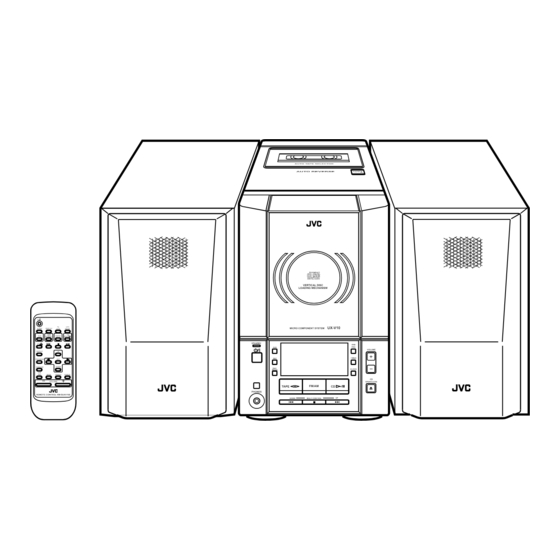
UX-V10GN UX-V10GN SERVICE MANUAL MICRO COMPONENT SYSTEM UX-V10GN AUTO T APE SELECTOR AUTO REVERSE T APE COMPACT DIGITAL AUDIO VERTICAL DISC LOADING MECHANISM SLEEP DISPLAY AUTO MICRO COMPONENT SYSTEM UX-V10 MODE PRESET TAPE FM/AM STANDBY VOLUME REPEAT TIMER PROGRAM RANDOM DOWN REV. -
Page 2: Safety Precautions
UX-V10GN Safety Precautions 1. This design of this product contains special hardware and many circuits and components specially for safety purposes. For continued protection, no changes should be made to the original design unless authorized in writing by the manufacturer. - Page 3 UX-V10GN Safety precautions (U.K only) 1. This design of this product contains special hardware and many circuits and components specially for safety purposes. For continued protection, no changes should be made to the original design unless authorized in writing by the manufacturer.
-
Page 4: Important For Laser Products
UX-V10GN Important for laser products 5.CAUTION : If safety switches malfunction, the laser is able 1.CLASS 1 LASER PRODUCT to function. 2.DANGER : Invisible laser radiation when open and inter 6.CAUTION : Use of controls, adjustments or performance of lock failed or defeated. Avoid direct exposure to beam. -
Page 5: Disassembly Method
UX-V10GN Disassembly method <Main body> Removing the rear cover (See Fig.1 and 2) Remove the eight screws A attaching the rear cover on the back of the body. Remove the two screws B attaching the rear cover on the bottom of the body. - Page 6 UX-V10GN Removing cassette mechanism Cassette mechanism assembly assembly (See Fig.5 and 6) Joint a Prior to performing the following procedure, remove the rear cover and the side panels. CN304 Disconnect the card wires from connector CN304 and CN305 on the main board on the left side of the CN305 body.
- Page 7 UX-V10GN Heat sink Main board Removing the front panel assembly (See Fig.10 to 12) Prior to performing the following procedure, remove Fig.9 the rear cover, the side panels, the cassette mechanism assembly and the main board. Front panel assembly Disconnect the card wire from connector CN732 on the LCD board.
- Page 8 UX-V10GN Removing the tuner & function board (See Fig.14) Prior to performing the following procedure, remove the rear cover, the side panels and the cassette mechanism assembly. Disconnect the card wire from connector CN1 on the tuner & function board.
- Page 9 UX-V10GN <Cassette mechanism assembly> Prior to performing the following procedure, remove the rear cover, the side panels and the cassette Cassette door mechanism assembly. Removing the Opt.Dig.out board (See Fig.16) Remove the two screws K attaching the Opt.Dig.out board on the side of the cassette mechanism assembly.
- Page 10 UX-V10GN <Front panel assembly> CD mechanism cover Prior to performing the following procedure, remove (CD mechanism assembly) the rear cover, the side panels, the cassette mechanism assembly, the main board and the front panel assembly. Removing the CD mechanism assembly (See Fig.18 to 21)
- Page 11 UX-V10GN CD door switch board Removing the LED board (B) (See Fig.22) CD servo control Prior to performing the following procedure, remove Hook i board the CD mechanism assembly. Remove the screw P attaching the LED board (B). Removing the CD door switch board (See Fig.22)
- Page 12 UX-V10GN <<Cassette Mechanism Section>> Cassette mechanism Removing the Playback/Recording & Eraser Head ( See Figs. 1 and 2 ) 1. While shifting the trigger arms seen on the right side of the head mount in the arrow direction, turn the flywheel R in counterclockwise direction...
- Page 13 UX-V10GN Removing the Head amplifier & Mechanism control P.C. board Belt (See Fig. 4) Main motor 1. Remove the cassette mechanism assembly. assembly 2. After turning over th cassette mechanism assembly, remove the three screws "1" retaining the head amplifier & mechanism control P.C. board.
- Page 14 UX-V10GN Removing the Flywheel (See Figs. 7 and 8) Flywheel R Flywheel L 1. Remove the head amplifier & mechanism control P.C. board. 2. Remove the main motor assembly. 3. After turning over the cassette mechanism, remove the slit washers "b" and "c" fixing the capstan shafts R and L, and pull out the flywheel R and L respectively from behind the cassette mechanism.
-
Page 15: Main Adjustment
UX-V10GN Main adjustment Measurement Instruments Required for Tuner section Adjustment B/E/EN version FM Band cover: 87.5 108MHz 1. Low frequency oscillator This oscillator should have a capacity to output MW Band cover: 522 1,629kHz 0dBs to 600 at an oscillation frequency of... - Page 16 UX-V10GN << >> Arrangement of Adjusting Position Cassette mechanism section Cassette mechanism section (Back side) Head azimuth Head azimuth adjusting screw adjusting screw (Forward side) (Reverse side) Head azimuth Head azimuth Playback/Recording & adjusting screw adjusting screw eraser head (Forward side)
- Page 17 UX-V10GN Tape Recorder Section Measurement Adjusting Standard Items Measurement method conditions positions Values Adjust the head Confirmation Test tape 1 Playback the test tape VTT703L (8kHz) Maximum azimuth screw of head angle : VTT703L (8kHz) 2 With the recording & playback mechanism,...
- Page 18 UX-V10GN Electrical Performance Adjusting Measurement Standard Items Measurement method positions conditions Values L ch AC-225 Adjustment of Mode: Forward or 1 With the recording and playback : VR101 : 4.20 recording bias reverse mode mechanism, load the test tapes (AC-514 to...
-
Page 19: Flow Of Functional Operation Until Toc Read
UX-V10GN Flow of functional operation until TOC read Check Point Slider turns REST Power Key Power ON Check that the voltage at the pin17 SW ON. of CN604 is 0V (a moment)? Automatic tuning of TE offset Check that the voltage at the... -
Page 20: Maintenance Of Laser Pickup
UX-V10GN Maintenance of laser pickup Replacement of laser pickup (1) Cleaning the pick up lens Befor you replace the pick up, please try to Turn off the power switch and,disconnect the clean the lens with a alcohol soaked cotton power cord from the ac outlet. -
Page 21: Description Of Major Ics
UX-V10GN Description of major ICs LA6541-X(IC541) : Servo Driver 1. Pin Layout & Block Diagram Vref Vin4 Vin3 Level B T L B T L Level RESET shift driver driver shift Level B T L B T L Level Regulator... - Page 22 UX-V10GN MN35510 (IC651) : DIGITAL SERVO&DIGITAL SIGNAL PROCESSER 1. Terminal Layout 20 ~ 41 ~ 2.Block Diagram LRCKIN(MSEL) AVSS1 8TIMES BCLK(SSEL) AVDD1 DIGITAL OVER SAMPUNC SRDATAIN OUTR DEEMPHSIS DIGITAL FILTER 1BIT (PSEL) LOGIC IOSEL CLVS BLKCK OUTL CLDCK SBCK SUBC...
- Page 23 UX-V10GN 3. Description symbol I/O Description symbol I/O Description BCLK Not used Tracking error shunt signal output(H:shunt) LRCK Not used PLAY Not used SRDATA Not used WVEL Not used DVDD1 Power supply (Digital) RF signal input DVSS1 Connected to GND...
- Page 24 UX-V10GN AN8806SB-W(IC301) :RF&SERVO AMP 1.Pin layout PD 1 36 PDAC 35 PDBD LD 2 LDON 3 34 PDF 33 PDE LDP 4 VCC 5 32 PDER 31 PDFR RF- 6 30 TBAL RF OUT 7 29 FBAL RF IN 8 28 EF- C.AGC 9...
- Page 25 UX-V10GN 3. Pin function Pin No. symbol Function APC amp . Input terminal APC amp . Output terminal LD ON LD ON/OFF control terminal Connect to GND Power supply RF amp . Reversing input terminal RFamp . Output terminal RF OUT...
- Page 26 UX-V10GN UPD78064GF-108 (IC701): System CPU 1.Pin layout 2.Pin function Symbol Function Symbol Function [RESET/CLOSE] switch USDATA Serial data URESET/CLOSE Abnormal voltage detection 1 USCK Serial clock USAFETY1 Abnormal voltage detection 2 UQRIN CD Q code data USAFETY0 Body key input 1...
- Page 27 UX-V10GN LA1838(IC102): FM AM IF AMP&detector, FM MPX Decoder 1. Block Diagram DECODER RF.AMP ANIT-BIRDIE MUTE BUFF STEREO P-DET AM IF PILOT 384KHz COMP S-METER AM/FM S-CLRVE S-METER IF-BUFF TUNING STEREO DRIVE DRIVE FM IF 2. Pin Function Symbol Function...
- Page 28 UX-V10GN LC72136N (IC121) : PLL Frequency Synthesizer 1. Pin layout FM/AM LPFOUT LPFIN CLOCK FM/ST/VCO FMIN AM/FM AMIN IFCONT SDIN IFIN 2. Block diagram Phase Reference Detector Driver Charge Pump Swallow Counter Swallow Counter 1/16,1/17 4bit 1/16,1/17 4bit Unlock Detector...
- Page 29 UX-V10GN BA15218N (IC342/IC343/IC391/IC453IC362/IC363) : Dual Ope. Amp. OUT1 +IN1 +IN1 GND +IN2 -IN2 OUT2 Vcc BU4094BCF-X(IC304,IC303):Serial to parallel port extension 1.Pin layout 2.Block diagram STROBE DATA OUTPUT ENABLE DATA 8-STAGE CLOCK SERIAL SHIFT REGISTER OUTPUT CLOCK 8-BIT STROBE LATHES 3-STATE...
- Page 30 UX-V10GN GP1U271X (IC701) : Receiver for remote – Limiter Integrator Comparator Amp. Demodulator B.P.F Vout LB1641 (IC501) : DC Motor Driver 1. Pin Layout GND OUT1 P1 IN2 VCC1 VCC2 P2 OUT2 2. Pin Functions Input Output Mode OUT1 OUT2...
- Page 31 UX-V10GN AN7345(IC302) PB/REC AMP NF1 OUT1 CTL1 RIN1 RNF1 ROUT1 REPPLE Source CTRL CTRL EQ2 CTL2 OUT2 RIN2 RNF2 ROUT2 2. Pin Function Symbol Function Symbol Function Power supply Playback amplifier input Repple filter Playback amplifier input EQCTL EQ control...
- Page 32 UX-V10GN LC75342 1-32...
- Page 33 UX-V10GN 3. Pin function Pin No. symbol Function Serial data input pin for control Chip enable pin Ground TEST TEST pin for electronic volume control LOUT Volume+equalizer output Bas-band filter comprising capacitor and resistor connection LBASS2 LBASS1 Bas-band filter comprising capacitor and resistor connection...
- Page 34 UX-V10GN LC72723 Pin Assignment Block diagram VREF FLOUT CIN Vdda CLOCK Vddd RECOVERY REFERENCE (57kHz) (1187.5kHz) VOLTAGE Vssa VREF Vssd 57kHz ANTIALIASING DATA SMOOTHING RDDA MPXIN (SCF) FILTER FILTER DECODER RDCL MDDE (128-bits) CLK(4.332MHz) RDS-ID RDS-ID/ TEST TEST TEST DETECT...
- Page 35 UX-V10GN UX-V10GN VICTOR COMPANY OF JAPAN, LIMITED AUDIO & COMMUNICATION BUSINESS DIVISION PERSONAL & MOBILE NETWORK BUSINESS UNIT 10-1,1Chome,Ohwatari-machi,Maebashi-city,371-8543,Japan Printed in Japan 1-35 No.20886 200012(O)
Need help?
Do you have a question about the UX-V10GN and is the answer not in the manual?
Questions and answers