Table of Contents
Advertisement
QQ
3 7 63 1515 0
SERVICE MANUAL
Ver 1.0 2002. 04
This set is the tuner, deck, CD and amplifier
section in CHC-TB10.
TE
L 13942296513
Amplifier section
European models
DIN power output (Rated):40 + 40 watts
Continuous RMS power output (Reference):
Music power output (Reference):
Other models
Measured at AC 120/220/240 V, 50/60 Hz:
DIN power output (Rated):40 + 40 watts
Continuous RMS power output (Reference):
Inputs
MD IN (phono jacks):
Outputs
PHONES (stereo minijack):
SPEAKER:
CD player section
System
www
Laser
.
Sony Corporation
9-873-944-01
2002D1600-1
Home Audio Company
© 2002.04
Published by Sony Engineering Corporation
http://www.xiaoyu163.com
TAPE DECK
Frequency response
CD DIGITAL OUT
(Square optical connector jack, rear panel)
Wavelength
Tape deck section
(6 ohms at 1 kHz, DIN)
Recording system
50 + 50 watts
Frequency response
(6 ohms at 1 kHz, 10%
THD)
Tuner section
100 + 100 watts
FM stereo, FM/AM superheterodyne tuner
(6 ohms at 1 kHz, 10%
THD)
FM tuner section
Tuning range
Antenna
Antenna terminals
(6 ohms at 1 kHz, DIN)
Intermediate frequency
50 + 50 watts
AM tuner section
(6 ohms at 1 kHz, 10%
Tuning range
THD)
European models:
voltage 450 mV,
impedance 47 kilohms
Pan-American models:
accepts headphones of
8 ohms or more.
Accepts impedance of 6 to
16 ohms.
Compact disc and digital
audio system
Semiconductor laser
(λ=780 nm)
Emission duration:
x
ao
u163
y
continuous
i
http://www.xiaoyu163.com
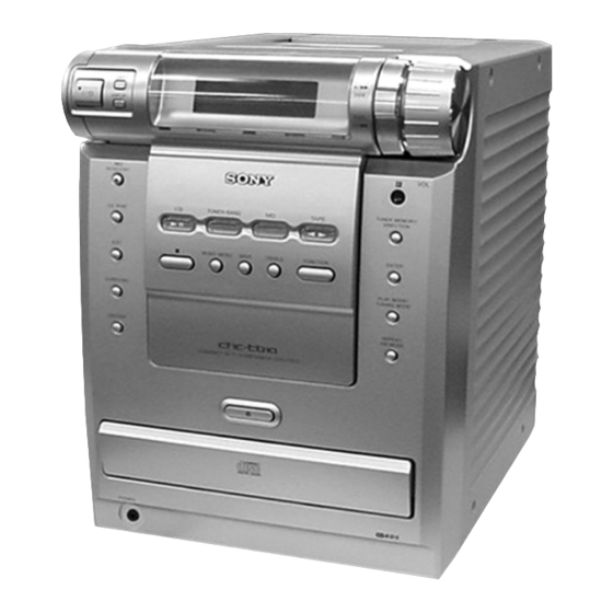
HCD-TB10
2 9
8
Model Name Using Similar Mechanism
CD
CD Mechanism Type
SECTION
Optical Pick-up Block Type
Model Name Using Similar Mechanism
SECTION
Tape Transport Mechanism Type
Q Q
3
6 7
1 3
SPECIFICATIONS
2 Hz – 20 kHz (±0.5 dB)
660 nm
4-track 2-channel stereo
50 – 13,000 Hz (±3 dB),
using Sony TYPE I
cassettes
87.5 – 108.0 MHz
(50 kHz step)
FM lead antenna
75 ohms unbalanced
10.7 MHz
531 – 1,602 kHz
(with the interval set at
9 kHz)
531 – 1,710 kHz
(with the interval set at
9 kHz)
530 – 1,710 kHz
(with the interval set at
10 kHz)
COMPACT HiFi COMPONENT SYSTEM
.
9 4
2 8
AEP Model
UK Model
NEW
CDM55C-K6A
KSM-213DCP
NEW
CMAL1Z222A
1 5
0 5
8
2 9
9 4
Other models:
531 – 1,602 kHz
(with the interval set at
9 kHz)
530 – 1,710 kHz
(with the interval set at
10 kHz)
Antenna
AM loop antenna
External antenna terminals
Intermediate frequency
450 kHz
General
Power requirements
European models:
230 V AC, 50/60 Hz
Mexican model:
120 V AC, 60 Hz
Other models:
120 V, 220 V, 230 –
240 V AC, 50/60 Hz
Adjustable with voltage
selector
Power consumption
European models:
100 watts
0.5 watts (at the Power
Saving Mode)
Other models:
100 watts
Dimensions (w/h/d) incl. projecting parts and controls
Amplifier/Tuner/Tape/CD section:
Approx. 215 × 285 ×
334 mm
Mass
Amplifier/Tuner/Tape/CD section:
Approx. 6.5 kg
Design and specifications are subject to change
without notice.
m
co
9 9
E Model
2 8
9 9
Advertisement
Table of Contents

Related Manuals for Sony HCD-TB10


Summary of Contents for Sony HCD-TB10
- Page 1 Design and specifications are subject to change System Compact disc and digital without notice. audio system Laser Semiconductor laser COMPACT HiFi COMPONENT SYSTEM (λ=780 nm) Emission duration: u163 continuous Sony Corporation 9-873-944-01 2002D1600-1 Home Audio Company © 2002.04 Published by Sony Engineering Corporation http://www.xiaoyu163.com...
-
Page 2: Table Of Contents
HCD-TB10 3 7 63 1515 0 TABLE OF CONTENTS 1. SERVICING NOTES 6. DIAGRAMS ······················································· 3 ······································································ 19 6-1. Circuit Boards Location ············································· 19 2. GENERAL 6-2. Block Diagrams ·························································· 21 ·········································································· 5 6-3. Printed Wiring Board – MAIN Section – ·················· 23 6-4. -
Page 3: Servicing Notes
LIST ARE CRITICAL TO SAFE OPERATION. REPLACE THESE circuit board (within 3 times). COMPONENTS WITH SONY PARTS WHOSE PART NUMBERS • Be careful not to apply force on the conductor when soldering APPEAR AS SHOWN IN THIS MANUAL OR IN SUPPLEMENTS or unsoldering. - Page 4 HCD-TB10 3 7 63 1515 0 Service position of the TAPE cassette mechanism deck MAIN board Jig cord : J-2501-082-A CN404 TC Deck section L 13942296513 u163 http://www.xiaoyu163.com...
-
Page 5: General
HCD-TB10 SECTION 2 This section is extracted GENERAL 3 7 63 1515 0 from instruction manual. A – G A – G M – Z M – Z BASS wa (18) CD ql (9) MD 0 (24) MD 9 (24) -
Page 6: Setting The Clock
HCD-TB10 3 7 63 1515 0 Setting the clock Loading a CD Turn on the system. Press Z. The disc tray opens. Press CLOCK/TIMER SET on the remote. Place a CD with the label side up on the “CLOCK” appears. -
Page 7: Disassembly
HCD-TB10 SECTION 3 DISASSEMBLY 3 7 63 1515 0 • The equipment can be removed using the following procedure. SIDE PANEL TOP PANEL • The dotted square with arrow ( ) prompts you to move to the next job when all of the works within the dotted square ( )are completed. -
Page 8: Side Panel
HCD-TB10 3 7 63 1515 0 3-1. Side Panel 4 two screws 6 side panel (L) ( +BVTP 3 × 10 ) (Remove in the direction of the arrow.) 1 two screws ( +BVTP 3 × 10 ) 5 four screws... -
Page 9: Cassette Mechanism (Cmal1Z222A)
HCD-TB10 3 7 63 1515 0 3-3. Cassette Mechanism (CMAL1Z222A) 6 flat cable (9 core) 2 two screws ( +BVTP 2.6 × 8 ) 7 cassette mechanism deck (CMAL1Z222A) 1 two screws ( +BVTP 2.6 × 8 ) 4 screw ( +PTPWH 2.6 ×... -
Page 10: H/P Board, Panel Board
HCD-TB10 3 7 63 1515 0 3-5. H/P Board, PANEL Board front panel assy qf flat cable (39 core) (CN607) 9 three claws qs PANEL board (Remove in the direction of the arrow.) qd connector 6 two screws (CN611) ( +BVTP 2.6 ×... -
Page 11: Vol Board
HCD-TB10 3 7 63 1515 0 3-7. VOL Board Note: daring reassembling when flange. spring sub panel flange 6 VOL board 4 spring 5 shuttle 3 flange 2 nut 1 knob (vol) L 13942296513 3-8. SUB TRANSFORMER Board, Back Panel... -
Page 12: Main Board
HCD-TB10 3 7 63 1515 0 3-9. MAIN Board 5 MAIN Board 3 connector (CN906) 4 connector (CN402) 2 connector (CN734) 1 two screws ( +BVTP 3 × 10 ) MAIN board CN501 (Pull out MAIN board.) CN402 3-10. CDM Board, CD Mechanism Deck... -
Page 13: Power Trans Former, P-Amp Board
HCD-TB10 3 7 63 1515 0 3-11. Power Trans Former, P-AMP Board 5 three screws ( +BVTP 2.6 × 8 ) 3 four screws (+BVTT 4 × 6) 4 power transformer 6 P- AMP board 1 connector (CN906) 2 screw ( +BVTP 2.6 ×... -
Page 14: Motor (Tray) Board
HCD-TB10 3 7 63 1515 0 3-13. MOTOR (TRAY) Board 1 two screws ( M 2.6 ) 2 MOTOR (TRAY) board L 13942296513 3-14. Holder Assy 1 floating screw (PTPWH M2.6) 2 Remove the Holder (BU) assy in the direction of arrow A . -
Page 15: Motor Board
HCD-TB10 3 7 63 1515 0 3-15. MOTOR Board 1 Remove the four solders. M101 M102 2 MOTOR board L 13942296513 u163 http://www.xiaoyu163.com... -
Page 16: Test Mode
HCD-TB10 SECTION 4 TEST MODE 3 7 63 1515 0 [Change-over of AM Tuner Step between 9 kHz and 10 kHz] The message “KEY0 0 0” is displayed. • A step of AM channels can be changed over between 9 kHz and Each time a button is pressed, the key code number is displayed. -
Page 17: Electrical Adjustments
HCD-TB10 SECTION 5 ELECTRICAL ADJUSTMENTS 3 7 63 1515 0 FM Tuned Level Adjustment TUNER SECTION FM RF Signal generator AM IF Adjustment 75 Ω coaxial AM RF Signal generator Carrier frequency : 98 MHz Modulation : AUDIO 1 kHz, 75 kHz... - Page 18 HCD-TB10 3 7 63 1515 0 CD SECTION Note : 1. CD Block is basically designed to operate without adjustment. Therefore, check each item in order given. 2. Use YEDS-18 disc (3-702-101-01) unless otherwise indicated. 3. Use an oscilloscope with more than 10MΩ impedance.
-
Page 19: Diagrams
HCD-TB10 SECTION 6 DIAGRAMS 3 7 63 1515 0 6-1. Circuit Boards Location SUB TRANSFORMER board BACK LIGHT board PANEL board LCD board VOL board H/P board MAIN board L 13942296513 POWER TRANSFORMER board CDM board u163 P-AMP board... - Page 20 HCD-TB10 3 7 63 1515 0 • Waveforms THIS NOTE IS COMMON FOR PRINTED WIRING BOARDS AND SCHEMATIC DIAGRAMS. IC751 rf (XOUT) (In addition to this, the necessary note is printed in each block.) For schematic diagrams. Note: • All capacitors are in µF unless otherwise noted. pF: µµF 5.9 Vp-p...
-
Page 21: Block Diagrams
HCD-TB10 6-2. Block Diagrams 3 7 6 3 1 5 1 5 0 MAIN Section AUDIO SOUND PROCESSOR IC501 IC301 POWER AMP JK401 IC302 TUNER L-CH SECTION OUT1 SPEAKER RY401 Q408,409 R CH OUT2 R-CH CD-L RELAY Q309 Q305... - Page 22 HCD-TB10 TUNER/CD Section 3 7 6 3 1 5 1 5 0 EXCEPT AEP,UK MODEL AM/FM IF MPX JK101 FE101 Q101 IC101 CF101 CF102 RF IF L-CH ANT IN IF OUT FM IF L OUT FM 75Ω OSC OUT...
-
Page 23: Printed Wiring Board - Main Section
HCD-TB10 6-3. Printed Wiring Board – MAIN Section – • See page 19 for Circuit Boards Location. 3 7 6 3 1 5 1 5 0 MAIN BOARD DIGITAL SPEAKER ANTENNA PH401 AEP,UK E,MX, TW,KR • Semiconductor Location Ref. No. Location Ref. -
Page 24: Schematic Diagram - Main Section (1/4)
HCD-TB10 6-4. Schematic Diagram – MAIN Section (1/4) – • See page 37, 38 for IC Block Diagrams. • See page 20 for Waveforms. 3 7 6 3 1 5 1 5 0 MAIN BOARD (1/4) (EXCEPT AEP,UK) (AEP,UK) -
Page 25: Schematic Diagram - Main Section (2/4)
HCD-TB10 6-5. Schematic Diagram – MAIN Section (2/4) – • See page 38 for IC Block Diagrams. 3 7 6 3 1 5 1 5 0 TO CDM (3/4) BOARD (Page 26) CN743 (Page 34) PH401 DIGITAL 1 2 3... -
Page 26: Schematic Diagram - Main Section (3/4)
HCD-TB10 6-6. Schematic Diagram – MAIN Section (3/4) – • See page 20 for Waveforms. 3 7 6 3 1 5 1 5 0 (1/4) (2/4) (2/4) (Page 24) (Page 25) (Page 25) 9 10 12 13 14 15... -
Page 27: Schematic Diagram - Main Section (4/4)
HCD-TB10 6-7. Schematic Diagram – MAIN Section (4/4) – 3 7 6 3 1 5 1 5 0 (2/4) (2/4) (2/4) (Page 25) (Page 25) (Page 25) MAIN BOARD (4/4) IC401 +10V REG 18.6 TRIG DRIVE TRIG DRIVE (3/4) -
Page 28: Schematic Diagram - Panel Section
HCD-TB10 6-8. Schematic Diagram – PANEL Section – • See page 39 for IC Pin Function Description. • See page 20 for Waveforms. 3 7 6 3 1 5 1 5 0 MAIN BOARD (4/4) CN403 (Page 27) VOL BOARD... -
Page 29: Printed Wiring Board - Panel Section
HCD-TB10 6-9. Printed Wiring Board – PANEL Section – • See page 19 for Circuit Boards Location. 3 7 6 3 1 5 1 5 0 PANEL BOARD LCD BOARD VOL BOARD CN608 CN612 (Page 30) (Page 30) RM601... -
Page 30: Printed Wiring Board - Lcd Section
HCD-TB10 6-10. Printed Wiring Board – LCD Section – • See page 19 for Circuit Boards Location. 3 7 6 3 1 5 1 5 0 PANEL BOARD CN607 (Page 29) LCD BOARD VOL BOARD C617 1-683-961- (11) (11) -
Page 31: Schematic Diagram - Amp/Power Section
HCD-TB10 6-11. Schematic Diagram – AMP/POWER Section – 3 7 6 3 1 5 1 5 0 POWER TRANSFORMER BOARD P-AMP BOARD T901 POWER TRANS 6.3A/250V 6.3A/250V 3.15A/250V 2A/250V AEP, MAIN BOARD (3/4) MAIN CN401 BOARD (Page 26) (3/4) -
Page 32: Printed Wiring Board - Amp Section
HCD-TB10 6-12. Printed Wiring Board – AMP Section – • See page 19 for Circuit Boards Location. 3 7 6 3 1 5 1 5 0 P-AMP BOARD 1 3 9 4 2 2 9 6 5 1 3 •... -
Page 33: Printed Wiring Board - Power Section
HCD-TB10 6-13. Printed Wiring Board – POWER Section – • See page 19 for Circuit Boards Location. 3 7 6 3 1 5 1 5 0 POWER TRANSFORMER BOARD P-AMP BOARD CN502 (Page 32) SUB TRANSFORMER BOARD T902 MAIN... -
Page 34: Schematic Diagram - Cd Section
HCD-TB10 6-14. Schematic Diagram – CD Section – • See page 36, 37 for IC Block Diagrams. • See page 20 for Waveforms. 3 7 6 3 1 5 1 5 0 CDM BOARD OPTICAL PICK-UP CN733 BLOCK KSM-213DCP... -
Page 35: Printed Wiring Board - Cd Section
HCD-TB10 6-15. Printed Wiring Board – CD Section – • See page 19 for Circuit Boards Location. 3 7 6 3 1 5 1 5 0 CDM BOARD PANEL BOARD CN602 (Page 29) IC751 17 16 1 3 9 4 2 2 9 6 5 1 3... -
Page 36: Printed Wiring Board - Motor Section
HCD-TB10 6-16. Printed Wiring Board – MOTOR Section – • See page 19 for Circuit Boards Location. • IC Block Diagrams 3 7 6 3 1 5 1 5 0 IC731 LA9242M 58 57 55 54 53 52 51 50... - Page 37 HCD-TB10 3 7 63 1515 0 IC781 BA5810FP-E2 BIAS LOADING PRE OPIN4+ FWD REV – OPIN4– LDCONT POWER OPOUT4 SAVE OPIN3+ – OPIN3– PREVCC (PRE.LOADING) OPOUT3 PREVCC POWVCC12 (CH1.CH2) CH1-4 MUTE POWVCC MUTE POWVCC34 (CH3,CH4) VOL– POWVCC VOL+ –...
- Page 38 HCD-TB10 3 7 63 1515 0 IC102 LC72131D PHASE DETECTOR CHARGE PUMP POWER REFERENCE UNLOCK DIVIDER DETECTOR RESET SWALLOW COUNTER 1/16, 1/17 4BITS 12BITS PROGRAMMABLE DRIVER UNIVERSAL DATA SHIFT REGISTER LATCH INTERFACE COUNTER 3 4 5 6 7 8 9 10...
-
Page 39: Ic Pin Function Description
HCD-TB10 3 7 63 1515 0 6-17. IC Pin Function Description • IC601 LC877348A-5Z50E Master Control (PANEL Board) Pin No. Pin Name Description LC72131-CE Chip select signal output to the PLL tuner IC BD8371-DATA Data/latch signal output to the sound processor... - Page 40 HCD-TB10 3 7 63 1515 0 Pin No. Pin Name Description 44 to 53 S01 to S10 Segment drive signal output to the liquid crystal display VDD2 – Power supply VSS2 – Ground 56 to 78 S11 to S33 Segment drive signal output to the liquid crystal display –...
-
Page 41: Exploded Views
HCD-TB10 SECTION 7 EXPLODED VIEWS 3 7 63 1515 0 NOTE: • -XX, -X mean standardized parts, so they may • The mechanical parts with no reference number The components identified by mark 0 or have some differences from the original one. -
Page 42: Front Panel Section
Description Remarks Ref. No. Part No. Description Remarks 4-237-501-11 WINDOW 4-231-670-11 SPRING (CD) 4-962-708-52 EMBLEM (4-A), SONY 4-237-512-11 LID, CD 1-683-963-11 VOL BOARD 4-237-509-11 BUTTON (REC) 4-237-504-01 KNOB (VOL) 1-683-959-11 H/P BOARD 4-237-530-01 SPRING A-4729-704-A PANEL BOARD, COMPLETE 4-237-505-01 SHUTTLE... -
Page 43: Chassis Section
HCD-TB10 3 7 63 1515 0 7-3. Chassis Section supplied T901 F906 F905 F907 F904 supplied L 13942296513 CD mechanism deck section supplied Ref. No. Part No. Description Remarks Ref. No. Part No. Description Remarks 4-238-354-01 HOLDER, PWB 0 F905 1-533-473-11 FUSE, GLASS TUBE (DIA. -
Page 44: Cd Mechanism Deck Section (Cdm55C-K6A)
HCD-TB10 3 7 63 1515 0 7-4. CD Mechanism Deck Section (CDM55C-K6A) not supplied M103 not supplied L 13942296513 not supplied not supplied Ref. No. Part No. Description Remarks Ref. No. Part No. Description Remarks 1-683-960-11 MOTOR (TRAY) BOARD... -
Page 45: Electrical Parts List
HCD-TB10 SECTION 8 BACK LIGHT ELECTRICAL PARTS LIST 3 7 63 1515 0 NOTE: • Due to standardization, replacements in the • RESISTORS When indicating parts by reference number, parts list may be different from the parts All resistors are in ohms. - Page 46 HCD-TB10 3 7 63 1515 0 Ref. No. Part No. Description Remarks Ref. No. Part No. Description Remarks C782 1-164-159-21 CERAMIC 0.1uF R715 1-249-430-11 CARBON 1/4W C786 1-161-494-00 CERAMIC 0.022uF R716 1-249-439-11 CARBON 1/4W C787 1-104-665-11 ELECT 100uF 20.00% 10V...
- Page 47 HCD-TB10 MAIN 3 7 63 1515 0 Ref. No. Part No. Description Remarks Ref. No. Part No. Description Remarks R779 1-249-409-11 CARBON 1/4W F A-4729-701-A MAIN BOARD, COMPLETE (AEP,UK) R780 1-249-425-11 CARBON 4.7K 1/4W F A-4730-327-A MAIN BOARD, COMPLETE (E,MX,KR)
- Page 48 HCD-TB10 MAIN 3 7 63 1515 0 Ref. No. Part No. Description Remarks Ref. No. Part No. Description Remarks C157 1-162-306-11 CERAMIC 0.01uF 30.00% 16V C235 1-126-963-11 ELECT 4.7uF 20.00% 50V C158 1-162-211-31 CERAMIC 33PF C236 1-128-551-11 ELECT 22uF 20.00% 25V...
- Page 49 HCD-TB10 MAIN 3 7 63 1515 0 Ref. No. Part No. Description Remarks Ref. No. Part No. Description Remarks C411 1-126-767-11 ELECT 1000uF 20.00% 16V D416 8-719-991-33 DIODE 1SS133T-77 C412 1-126-916-11 ELECT 1000uF 20.00% 6.3V D418 8-719-991-33 DIODE 1SS133T-77...
- Page 50 HCD-TB10 MAIN 3 7 63 1515 0 Ref. No. Part No. Description Remarks Ref. No. Part No. Description Remarks Q305 8-729-119-78 TRANSISTOR 2SC2785TP-HFE R135 1-247-843-11 CARBON 3.3K 1/4W Q306 8-729-119-78 TRANSISTOR 2SC2785TP-HFE R136 1-249-429-11 CARBON 1/4W Q309 8-729-119-78 TRANSISTOR...
- Page 51 HCD-TB10 MAIN 3 7 63 1515 0 Ref. No. Part No. Description Remarks Ref. No. Part No. Description Remarks R231 1-249-437-11 CARBON 1/4W R348 1-249-421-11 CARBON 2.2K 1/4W F R232 1-249-409-11 CARBON 1/4W F R349 1-249-425-11 CARBON 4.7K 1/4W F...
- Page 52 HCD-TB10 MAIN MOTOR MOTOR (TRAY) PANEL 3 7 63 1515 0 Ref. No. Part No. Description Remarks Ref. No. Part No. Description Remarks < ADJ > * CN611 1-564-720-11 PIN, CONNECTOR (SMALL TYPE) 4P SFR101 1-241-765-11 RES, ADJ, CARBON 22K <...
- Page 53 HCD-TB10 PANEL P-AMP 3 7 63 1515 0 Ref. No. Part No. Description Remarks Ref. No. Part No. Description Remarks R634 1-247-843-11 CARBON 3.3K 1/4W S610 1-762-196-21 SWITCH, TACT (FM MODE/REPEAT) R635 1-249-432-11 CARBON 1/4W R638 1-249-428-11 CARBON 8.2K...
- Page 54 HCD-TB10 P-AMP POWER TRANSFORMER SUB TRANSFORMER 3 7 63 1515 0 Ref. No. Ref. No. Part No. Part No. Description Description Remarks Remarks Ref. No. Ref. No. Part No. Part No. Description Description Remarks Remarks < TERMINAL > < FUSE >...
- Page 55 HCD-TB10 3 7 63 1515 0 Ref. No. Part No. Description Remarks < RESISTOR > R682 1-249-421-11 CARBON 2.2K 1/4W F R683 1-247-843-11 CARBON 3.3K 1/4W < SWITCH > S623 1-786-289-11 SWITCH, DETECTION (+/-) <VARIABLERESISTOR > VR601 1-473-534-11 ENCODER, ROTARY (VOL)
- Page 56 HCD-TB10 3 7 63 1515 0 REVISION HISTORY Clicking the version allows you to jump to the revised page. Also, clicking the version at the upper right on the revised page allows you to jump to the next revised page.
Need help?
Do you have a question about the HCD-TB10 and is the answer not in the manual?
Questions and answers