Table of Contents
Advertisement
HCD-GRX9000/RX900
SERVICE MANUAL
HCD-GRX9000/RX900 are the Amplifier,
CD player, Tape Deck and Tuner section
in MHC-GRX9000/RX900.
Dolby noise reduction manufactured under license
from Dolby Laboratories Licensing Corporation.
"DOLBY" and the double-D symbol a are trade-
marks of Dolby Laboratories Licensing Corporation.
MICROFILM
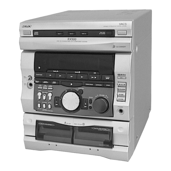
Photo: HCD-RX900
Model Name Using Similar Mechanism
CD
CD Mechanism Type
Section
Base Unit Type
Optical Pick-up Type
Model Name Using Similar Mechanism HCD-GRX7/RX77S
TAPE
DECK
Tape Transport Mechanism Type
Section
SPECIFICATIONS
MINI Hi-Fi COMPONENT SYSTEM
East European Model
CIS Model
HCD-RX900
E Model
HCD-GRX9000
HCD-H991AV
CDM38LH-5BD29AL
BU-5BD29AL
KSS-213D/Q-NP
TCM-230AWR1/
230PWR1
– Continued on next page –
Advertisement
Table of Contents

Related Manuals for Sony HCD-GRX9000


Summary of Contents for Sony HCD-GRX9000
- Page 1 HCD-GRX9000/RX900 SERVICE MANUAL East European Model CIS Model HCD-RX900 E Model HCD-GRX9000 HCD-GRX9000/RX900 are the Amplifier, CD player, Tape Deck and Tuner section Photo: HCD-RX900 in MHC-GRX9000/RX900. Dolby noise reduction manufactured under license Model Name Using Similar Mechanism HCD-H991AV from Dolby Laboratories Licensing Corporation.
- Page 1 HCD-GRX9000/RX900 SERVICE MANUAL East European Model CIS Model HCD-RX900 E Model HCD-GRX9000 HCD-GRX9000/RX900 are the Amplifier, CD player, Tape Deck and Tuner section Photo: HCD-RX900 in MHC-GRX9000/RX900. Dolby noise reduction manufactured under license Model Name Using Similar Mechanism HCD-H991AV from Dolby Laboratories Licensing Corporation.
- Page 2 – 2 –...
- Page 2 – 2 –...
-
Page 3: Table Of Contents
SECTION 1 SERVICING NOTES TABLE OF CONTENTS SERVICING NOTES ..........3 NOTES ON HANDLING THE OPTICAL PICK-UP BLOCK OR BASE UNIT GENERAL The laser diode in the optical pick-up block may suffer electro- Location of Controls ............6 static break-down because of the potential difference generated Setting the Time .............. -
Page 3: Table Of Contents
SECTION 1 SERVICING NOTES TABLE OF CONTENTS SERVICING NOTES ..........3 NOTES ON HANDLING THE OPTICAL PICK-UP BLOCK OR BASE UNIT GENERAL The laser diode in the optical pick-up block may suffer electro- Location of Controls ............6 static break-down because of the potential difference generated Setting the Time .............. - Page 4 LINE WITH MARK ! ON THE SCHEMATIC DIAGRAMS AND IN THE PARTS LIST ARE CRITICAL TO SAFE OPERATION. REPLACE THESE COMPONENTS WITH SONY PARTS WHOSE PART NUMBERS APPEAR AS SHOWN IN THIS MANUAL OR IN SUPPLEMENTS PUB- LISHED BY SONY.
- Page 4 LINE WITH MARK ! ON THE SCHEMATIC DIAGRAMS AND IN THE PARTS LIST ARE CRITICAL TO SAFE OPERATION. REPLACE THESE COMPONENTS WITH SONY PARTS WHOSE PART NUMBERS APPEAR AS SHOWN IN THIS MANUAL OR IN SUPPLEMENTS PUB- LISHED BY SONY.
- Page 5 HOW TO OPEN THE DISC TRAY WHEN POWER SWITCH TURNS OFF. 1 Remove the Case. 3 Pull-out the disc tray. 2 Turn the cam to the direction of arrow. NOTE FOR INSTALLATION (ROTARY ENCODER) Note:When attaching the Base unit, Insert the BU cam section A into the groove of BU cam.
- Page 5 HOW TO OPEN THE DISC TRAY WHEN POWER SWITCH TURNS OFF. 1 Remove the Case. 3 Pull-out the disc tray. 2 Turn the cam to the direction of arrow. NOTE FOR INSTALLATION (ROTARY ENCODER) Note:When attaching the Base unit, Insert the BU cam section A into the groove of BU cam.
-
Page 6: General
SECTION 2 GENERAL LOCATION OF CONTROLS 1 I /u (Power) button 2 DISC 1 to 3 buttons and indicators 3 DISC SKIP/EX-CHANGE button 4 6 (CD) button 5 CD disc tray 6 CD ^ button and indicator !∞ 7 TUNER, BAND button !§... -
Page 6: General
SECTION 2 GENERAL LOCATION OF CONTROLS 1 I /u (Power) button 2 DISC 1 to 3 buttons and indicators 3 DISC SKIP/EX-CHANGE button 4 6 (CD) button 5 CD disc tray 6 CD ^ button and indicator !∞ 7 TUNER, BAND button !§... - Page 7 – 7 –...
- Page 7 – 7 –...
-
Page 8: Disassembly
SECTION 3 DISASSEMBLY Note: Follow the disassembly procedure in the numerical order given. CASE 6 case 2 screw (CASE3 TP2) (3 × 12) 1 three screws (BVTT3 × 8) 3 two screws (CASE3 TP2) (3 × 8) 2 screw (CASE3 TP2) (3 × 12) 3 two screws (CASE3 TP2) (3 ×... -
Page 8: Disassembly
SECTION 3 DISASSEMBLY Note: Follow the disassembly procedure in the numerical order given. CASE 6 case 2 screw (CASE3 TP2) (3 × 12) 1 three screws (BVTT3 × 8) 3 two screws (CASE3 TP2) (3 × 8) 2 screw (CASE3 TP2) (3 × 12) 3 two screws (CASE3 TP2) (3 ×... - Page 9 TAPE MECHANISM DECK SECTION (TCM-230AWR1/TCM-230PWR1) 3 three screws (BVTP3 × 8) 4 two screws (BVTP3 × 8 ) 2 Open the cassette lids. 5 tape mechanism deck section (TCM-230AWR1/ TCM-230PWR1) 1 Push the cassette lids. CD MECHANISM DECK SECTION (CDM38LH-5BD29AL) 3 two screws (BVTP3 ×...
- Page 9 TAPE MECHANISM DECK SECTION (TCM-230AWR1/TCM-230PWR1) 3 three screws (BVTP3 × 8) 4 two screws (BVTP3 × 8 ) 2 Open the cassette lids. 5 tape mechanism deck section (TCM-230AWR1/ TCM-230PWR1) 1 Push the cassette lids. CD MECHANISM DECK SECTION (CDM38LH-5BD29AL) 3 two screws (BVTP3 ×...
- Page 10 MAIN BOARD 3 two screws 3 screw (BVTP3 × 8) (BVTP3 × 8) 2 wire (flat type) (13 core) (14 cm) (CN102) (E, Thai) wire (flat type) (15 core) (14 cm) (CN102) (EXCEPT E, Thai) 1 connector (CN11) 3 screw (BVTP3 ×...
- Page 10 MAIN BOARD 3 two screws 3 screw (BVTP3 × 8) (BVTP3 × 8) 2 wire (flat type) (13 core) (14 cm) (CN102) (E, Thai) wire (flat type) (15 core) (14 cm) (CN102) (EXCEPT E, Thai) 1 connector (CN11) 3 screw (BVTP3 ×...
-
Page 11: Test Mode
SECTION 4 TEST MODE [MC Cold Reset] [Change-over of AM Tuner Step between 9 kHz and 10 kHz] • The cold reset clears all data including preset data stored in the RAM to initial conditions. Execute this mode when returning •... -
Page 11: Test Mode
SECTION 4 TEST MODE [MC Cold Reset] [Change-over of AM Tuner Step between 9 kHz and 10 kHz] • The cold reset clears all data including preset data stored in the RAM to initial conditions. Execute this mode when returning •... - Page 12 [Aging Mode] 4. Aging mode in Tape Deck section This mode can be used for operation check of CD section and tape 1) Display state deck section. • No error occurs • If an error occurred: Display action now The aging operation stops and display status. •...
- Page 12 [Aging Mode] 4. Aging mode in Tape Deck section This mode can be used for operation check of CD section and tape 1) Display state deck section. • No error occurs • If an error occurred: Display action now The aging operation stops and display status. •...
-
Page 13: Mechanical Adjustments
SECTION 5 SECTION 6 MECHANICAL ADJUSTMENTS ELECTRICAL ADJUSTMENTS Precaution DECK SECTION 0 dB=0.775 V 1. Clean the following parts with a denatured alcohol-moistened swab: 1. Demagnetize the record/playback head with a head demagne- record/playback heads pinch rollers tizer. erase head rubber belts 2. -
Page 13: Mechanical Adjustments
SECTION 5 SECTION 6 MECHANICAL ADJUSTMENTS ELECTRICAL ADJUSTMENTS Precaution DECK SECTION 0 dB=0.775 V 1. Clean the following parts with a denatured alcohol-moistened swab: 1. Demagnetize the record/playback head with a head demagne- record/playback heads pinch rollers tizer. erase head rubber belts 2. - Page 14 2. Turn the adjustment screw and check output peaks. If the peaks DECK B Tape Speed Adjustment do not match for L-CH and R-CH, turn the adjustment screw Note: Start the Tape Speed adjustment as below after setting to the test so that outputs match within 1dB of peak.
- Page 14 2. Turn the adjustment screw and check output peaks. If the peaks DECK B Tape Speed Adjustment do not match for L-CH and R-CH, turn the adjustment screw Note: Start the Tape Speed adjustment as below after setting to the test so that outputs match within 1dB of peak.
- Page 15 DECK B REC Bias Adjustment 4. Mode: Record Procedure: MD/VIDEO (AUDIO) IN INTRODUCTION 315 Hz, 50 mV (–23.8 dB) When set to the test mode performed in Tape Speed Adjustment, AF OSC blank tape when the tape is rewound after recording, the “REC memory mode” 600 Ω...
- Page 15 DECK B REC Bias Adjustment 4. Mode: Record Procedure: MD/VIDEO (AUDIO) IN INTRODUCTION 315 Hz, 50 mV (–23.8 dB) When set to the test mode performed in Tape Speed Adjustment, AF OSC blank tape when the tape is rewound after recording, the “REC memory mode” 600 Ω...
-
Page 16: Tuner Section
TUNER SECTION 0 dB=1 µV (East European, CIS models only) Note: As a front-end (FE1) is difficult to repair if faulty, replace it with new one. MW Section Adjustment Note: FM Tuned Level Adjustment should be performed after this MW Tuned Level Adjustment. -
Page 16: Tuner Section
TUNER SECTION 0 dB=1 µV (East European, CIS models only) Note: As a front-end (FE1) is difficult to repair if faulty, replace it with new one. MW Section Adjustment Note: FM Tuned Level Adjustment should be performed after this MW Tuned Level Adjustment. - Page 17 FM Polar Adjustment Procedure : 1. Set the modulation of FM RF SSG to AUDIO 1 kHz, 10 kHz Connection 1: deviation according to “Connection 1”. 2. Tune the set to 69 MHz. FM RF SSG 3. Adjust the RV1702 so that the reading of frequency counter 75 Ω...
- Page 17 FM Polar Adjustment Procedure : 1. Set the modulation of FM RF SSG to AUDIO 1 kHz, 10 kHz Connection 1: deviation according to “Connection 1”. 2. Tune the set to 69 MHz. FM RF SSG 3. Adjust the RV1702 so that the reading of frequency counter 75 Ω...
-
Page 18: Cd Section
E-F Balance (Traverse) check CD SECTION (Without remote commander) Note: 1. CD Block is basically designed to operate without adjustment. There- oscilloscope fore, check each item in order given. BD board 2. Use YEDS-18 disc (3-702-101-01) unless otherwise indicated. 3. Use an oscilloscope with more than 10 MΩ impedance. TP (TEO) 4. -
Page 18: Cd Section
E-F Balance (Traverse) check CD SECTION (Without remote commander) Note: 1. CD Block is basically designed to operate without adjustment. There- oscilloscope fore, check each item in order given. BD board 2. Use YEDS-18 disc (3-702-101-01) unless otherwise indicated. 3. Use an oscilloscope with more than 10 MΩ impedance. TP (TEO) 4. - Page 19 Adjustment Location: [BD BOARD] (Conductor Side) IC101 IC103 CNU102 – 19 –...
- Page 19 Adjustment Location: [BD BOARD] (Conductor Side) IC101 IC103 CNU102 – 19 –...
-
Page 20: Diagrams
SECTION 7 DIAGRAMS • Circuit Boards Location TRANSFORMER board TCB board (East European, CIS) TUNER (FM / AM) (E, Saudi Arabia, Singapore, Malaysia) CD-SW board MAIN board AMP (R) board PANEL board AMP (L) board HP board SENSOR board MOTOR (TURN) board CONNECTOR board BD board MOTOR (SLIDE) board... -
Page 21: Block Diagram - Tuner Section (East European, Cis Models Only)
HCD-GRX9000/RX900 7-1. BLOCK DIAGRAM – TUNER Section (East European, CIS models only) – ST +10V • SIGNAL PATH : FM : AM (MW/LW) B+ SWITCH FM CIRCUIT B+ ANTENNA 10.7MHz 10.7MHz ST-L FM 75Ω FM IF AMP LPF41 OUT L... -
Page 21: Block Diagram - Tuner Section (East European, Cis Models Only)
HCD-GRX9000/RX900 7-1. BLOCK DIAGRAM – TUNER Section (East European, CIS models only) – ST +10V • SIGNAL PATH : FM : AM (MW/LW) B+ SWITCH FM CIRCUIT B+ ANTENNA 10.7MHz 10.7MHz ST-L FM 75Ω FM IF AMP LPF41 OUT L... -
Page 22: Block Diagram - Cd Section
HCD-GRX9000/RX900 7-2. BLOCK DIAGRAM – CD Section – DIGITAL SIGNAL PROCESSOR, FILTER CLV SERVO PROCESSOR, DIGITAL FILTER, D/A CONVERTER IC103 PD1 I-V AMP PCMDI PCMD OVER SERIAL BCKI SAMPLING INPUT DIGITAL LRCKI LRCK DETECTOR INTERFACE FILTER ASYMMETRY SUMMING DIGITAL PLL... -
Page 23: Block Diagram - Tape Deck Section
HCD-GRX9000/RX900 7-3. BLOCK DIAGRAM – TAPE DECK Section – DECK PROCESS DECK A/B SELECT, PB/REC EQ AMP, DOLBY NR AMP, ALC, AMS • SIGNAL PATH IC301 : PLAYBACK (DECK A) DOLBY PASS HP101 (PLAYBACK) : PLAYBACK (DECK B) PB OUT (L) -
Page 23: Block Diagram - Tape Deck Section
HCD-GRX9000/RX900 7-3. BLOCK DIAGRAM – TAPE DECK Section – DECK PROCESS DECK A/B SELECT, PB/REC EQ AMP, DOLBY NR AMP, ALC, AMS • SIGNAL PATH IC301 : PLAYBACK (DECK A) DOLBY PASS HP101 (PLAYBACK) : PLAYBACK (DECK B) PB OUT (L) -
Page 24: Block Diagram - Main Section (1/2)
HCD-GRX9000/RX900 7-4. BLOCK DIAGRAM – MAIN Section (1/2) – REC-L (Page 26) J101 (2/2) MD/VIDEO J751 (AUDIO) OUT MIX MIC R-CH MIC AMP MIC AMP • SIGNAL PATH R-CH IC750 (1/2) IC750 (2/2) : CD PLAY RV750 J191 LINE AMP... -
Page 24: Block Diagram - Main Section (1/2)
HCD-GRX9000/RX900 7-4. BLOCK DIAGRAM – MAIN Section (1/2) – REC-L (Page 26) J101 (2/2) MD/VIDEO J751 (AUDIO) OUT MIX MIC R-CH MIC AMP MIC AMP • SIGNAL PATH R-CH IC750 (1/2) IC750 (2/2) : CD PLAY RV750 J191 LINE AMP... -
Page 25: Block Diagram - Main Section (2/2)
HCD-GRX9000/RX900 7-5. BLOCK DIAGRAM – MAIN Section (2/2) – RELAY (Page 28) J421 PHONES • SIGNAL PATH : TUNER (FM/AM) L-CH L-CH (+) POWER AMP IC801 (1/2) (Page 28) – TM401 SPEAKER IMPEDANCE USE 8 – 16Ω – L-CH (–) -
Page 25: Block Diagram - Main Section (2/2)
HCD-GRX9000/RX900 7-5. BLOCK DIAGRAM – MAIN Section (2/2) – RELAY (Page 28) J421 PHONES • SIGNAL PATH : TUNER (FM/AM) L-CH L-CH (+) POWER AMP IC801 (1/2) (Page 28) – TM401 SPEAKER IMPEDANCE USE 8 – 16Ω – L-CH (–) -
Page 26: Block Diagram - Display/Key Control/Power Supply Section
HCD-GRX9000/RX900 7-6. BLOCK DIAGRAM – DISPLAY/KEY CONTROL/POWER SUPPLY Section – POWER FLUORESCENT INDICATOR TUBE DRIVE, (Page 27) LED DRIVE, KEY CONTROL IC601 CD-POWER (Page 27) DATA, CLK DATA FLUORESCENT INDICATOR TUBE FL601 (Page 27) RESET RESET (Page 28) CD MECHANISM DECK... -
Page 27: Note For Printed Wiring Boards And Schematic Diagrams
7-7. NOTE FOR PRINTED WIRING BOARDS AND SCHEMATIC DIAGRAMS (In addition to this, the necessary note is printed in each block.) Note on Schematic Diagram: Note on Printed Wiring Boards: • X : parts extracted from the component side. • All capacitors are in µF unless otherwise noted. pF: µµF •... -
Page 28: Printed Wiring Board - Tuner Section (East European, Cis Models Only)
7-8. PRINTED WIRING BOARD – TUNER Section (East European, CIS models only) – • See page 20 for Circuit Boards Location. • Semiconductor Location Ref. No. Location D1701 D1702 D1703 D1704 IC21 IC41 IC1701 IC1702 Q1701 Q1702 Q1703 MAIN BOARD CN102 (Page 52) –... -
Page 29: Schematic Diagram - Tuner Section (East European, Cis Models Only)
HCD-GRX9000/RX900 7-9. SCHEMATIC DIAGRAM – TUNER Section (East European, CIS models only) – • See page 75 for Waveforms. • See pages 76 and 77 for IC Block Diagrams. Note on Schematic Diagram: • Voltages and waveforms are dc with respect to ground (Page 57) under no-signal (detuned) conditions. -
Page 30: Printed Wiring Board - Cd Section
HCD-GRX9000/RX900 7-10. PRINTED WIRING BOARD – CD Section – • See page 20 for Circuit Boards Location. • Semiconductor Location Ref. No. Location IC101 IC102 IC103 Q101 MAIN BOARD CN105 (Page 51) – 37 – – 38 –... -
Page 30: Printed Wiring Board - Cd Section
HCD-GRX9000/RX900 7-10. PRINTED WIRING BOARD – CD Section – • See page 20 for Circuit Boards Location. • Semiconductor Location Ref. No. Location IC101 IC102 IC103 Q101 MAIN BOARD CN105 (Page 51) – 37 – – 38 –... -
Page 31: Schematic Diagram - Cd Section
HCD-GRX9000/RX900 7-11. SCHEMATIC DIAGRAM – CD Section – • See page 75 for Waveforms. • See pages 78 and 79 for IC Block Diagrams. (Page 53) MAIN BOARD CN105 Note on Schematic Diagram: Note: The components identified by mark ! or dotted line with mark ! are critical for safety. -
Page 32: Printed Wiring Boards - Cd Motor Section
HCD-GRX9000/RX900 7-12. PRINTED WIRING BOARDS – CD MOTOR Section – • See page 20 for Circuit Boards Location. (Page 51) MAIN BOARD CN104 (Page 51) MAIN BOARD CN103 – 41 – – 42 –... -
Page 32: Printed Wiring Boards - Cd Motor Section
HCD-GRX9000/RX900 7-12. PRINTED WIRING BOARDS – CD MOTOR Section – • See page 20 for Circuit Boards Location. (Page 51) MAIN BOARD CN104 (Page 51) MAIN BOARD CN103 – 41 – – 42 –... -
Page 33: Schematic Diagram - Cd Motor Section
HCD-GRX9000/RX900 7-13. SCHEMATIC DIAGRAM – CD MOTOR Section – • See page 80 for IC Block Diagrams. MAIN BOARD CN104 (Page 53) MTZJ-T72 –5.6C MTZJ-T-72-3.6B MAIN BOARD CN103 (Page 53) Note on Schematic Diagram: • Voltages are dc with respect to ground under no-signal conditions. -
Page 34: Printed Wiring Board - Tape Deck Section
HCD-GRX9000/RX900 7-14. PRINTED WIRING BOARD – TAPE DECK Section – • See page 20 for Circuit Boards Location. (Page 51) MAIN BOARD CN106 – 45 – – 46 –... -
Page 34: Printed Wiring Board - Tape Deck Section
HCD-GRX9000/RX900 7-14. PRINTED WIRING BOARD – TAPE DECK Section – • See page 20 for Circuit Boards Location. (Page 51) MAIN BOARD CN106 – 45 – – 46 –... -
Page 35: Schematic Diagram - Tape Deck Section
HCD-GRX9000/RX900 7-15. SCHEMATIC DIAGRAM – TAPE DECK Section – • See page 80 for IC Block Diagram. MAIN BOARD CN106 (Page 57) Note on Schematic Diagram: Note: The components identified by mark ! or dotted line with mark ! are critical for safety. -
Page 35: Schematic Diagram - Tape Deck Section
HCD-GRX9000/RX900 7-15. SCHEMATIC DIAGRAM – TAPE DECK Section – • See page 80 for IC Block Diagram. MAIN BOARD CN106 (Page 57) Note on Schematic Diagram: Note: The components identified by mark ! or dotted line with mark ! are critical for safety. -
Page 36: Printed Wiring Board - Leaf Sw Section
HCD-GRX9000/RX900 7-16. PRINTED WIRING BOARD – LEAF SW Section – • See page 20 for Circuit Boards Location. • Semiconductor Location Ref. No. Location Ref. No. Location D141 Q111 D333 Q112 D334 Q113 D401 G-10 Q161 D402 Q162 D403 F-11... -
Page 36: Printed Wiring Board - Leaf Sw Section
HCD-GRX9000/RX900 7-16. PRINTED WIRING BOARD – LEAF SW Section – • See page 20 for Circuit Boards Location. • Semiconductor Location Ref. No. Location Ref. No. Location D141 Q111 D333 Q112 D334 Q113 D401 G-10 Q161 D402 Q162 D403 F-11... -
Page 37: Printed Wiring Board - Main Section
HCD-GRX9000/RX900 7-18. PRINTED WIRING BOARD – MAIN Section – • See page 20 for Circuit Boards Location. (Page 34) (Page 41) (Page 41) (Page 38) (Page 45) (Page 49) (Page 61) (Page 67) (Page 73) (Page 70) – 51 –... -
Page 37: Printed Wiring Board - Main Section
HCD-GRX9000/RX900 7-18. PRINTED WIRING BOARD – MAIN Section – • See page 20 for Circuit Boards Location. (Page 34) (Page 41) (Page 41) (Page 38) (Page 45) (Page 49) (Page 61) (Page 67) (Page 73) (Page 70) – 51 –... -
Page 38: Schematic Diagram - Main Section (1/4)
HCD-GRX9000/RX900 7-19. SCHEMATIC DIAGRAM – MAIN Section (1/4) – (Page 55) (Page 40) (Page 44) (Page 44) (Page 59) Note on Schematic Diagram: • Voltages are dc with respect to ground under no-signal (detuned) conditions. (Page 57) no mark : FM ) : CD –... -
Page 39: Schematic Diagram - Main Section (2/4)
HCD-GRX9000/RX900 7-20. SCHEMATIC DIAGRAM – MAIN Section (2/4) – (Page 72) (Page 54) (Page 68) (Page 59) Note on Schematic Diagram: • Voltages are dc with respect to ground under no-signal Note: The components identified by mark ! or dotted line (detuned) conditions. -
Page 40: Schematic Diagram - Main Section (3/4)
HCD-GRX9000/RX900 7-21. SCHEMATIC DIAGRAM – MAIN Section (3/4) – (Page 53) (Page 35) (Page 48) (Page 59) (Page 50) Note on Schematic Diagram: • Voltages are dc with respect to ground under no-signal (detuned) conditions. no mark: FM ] : PB (DECK B) -
Page 40: Schematic Diagram - Main Section (3/4)
HCD-GRX9000/RX900 7-21. SCHEMATIC DIAGRAM – MAIN Section (3/4) – (Page 53) (Page 35) (Page 48) (Page 59) (Page 50) Note on Schematic Diagram: • Voltages are dc with respect to ground under no-signal (detuned) conditions. no mark: FM ] : PB (DECK B) -
Page 41: Schematic Diagram - Main Section (4/4)
HCD-GRX9000/RX900 7-22. SCHEMATIC DIAGRAM – MAIN Section (4/4) – • See page 75 for Waveforms. (Page 55) (Page 54) (Page 58) (Page 74) (Page 64) Note on Schematic Diagram: • Voltages are dc with respect to ground under no-signal (detuned) conditions. -
Page 41: Schematic Diagram - Main Section (4/4)
HCD-GRX9000/RX900 7-22. SCHEMATIC DIAGRAM – MAIN Section (4/4) – • See page 75 for Waveforms. (Page 55) (Page 54) (Page 58) (Page 74) (Page 64) Note on Schematic Diagram: • Voltages are dc with respect to ground under no-signal (detuned) conditions. -
Page 42: Printed Wiring Board - Panel Section
HCD-GRX9000/RX900 7-23. PRINTED WIRING BOARD – PANEL Section – • See page 20 for Circuit Boards Location. (Page 51) (Page 66) • Semiconductor Location Ref. No. Location Ref. No. Location Ref. No. Location Q610 D602 D651 Q618 D610 D652 Q620... -
Page 42: Printed Wiring Board - Panel Section
HCD-GRX9000/RX900 7-23. PRINTED WIRING BOARD – PANEL Section – • See page 20 for Circuit Boards Location. (Page 51) (Page 66) • Semiconductor Location Ref. No. Location Ref. No. Location Ref. No. Location Q610 D602 D651 Q618 D610 D652 Q620... -
Page 43: Schematic Diagram - Panel Section
HCD-GRX9000/RX900 7-24. SCHEMATIC DIAGRAM – PANEL Section – • See page 75 for Waveform. • See page 80 for IC Block Diagrams. (Page 60) (Page 65) Note on Schematic Diagram: • Voltages and waveforms are dc with respect to ground under no-signal (detuned) conditions. -
Page 44: Printed Wiring Board - Cd-Sw Section
HCD-GRX9000/RX900 7-25. PRINTED WIRING BOARD – CD-SW Section – • See page 20 for Circuit Boards Location. (Page 62) 7-26. SCHEMATIC DIAGRAM – CD-SW Section – (Page 64) Note on Schematic Diagram: • Voltages are dc with respect to ground under no-signal (detuned) conditions. -
Page 45: Printed Wiring Board - Hp Section
7-27. PRINTED WIRING BOARD – HP Section – • See page 20 for Circuit Boards Location. (Page 51) – 67 –... -
Page 45: Printed Wiring Board - Hp Section
7-27. PRINTED WIRING BOARD – HP Section – • See page 20 for Circuit Boards Location. (Page 51) – 67 –... -
Page 46: Schematic Diagram - Hp Section
7-28. SCHEMATIC DIAGRAM – HP Section – (Page 56) – 68 –... -
Page 46: Schematic Diagram - Hp Section
7-28. SCHEMATIC DIAGRAM – HP Section – (Page 56) – 68 –... -
Page 47: Printed Wiring Boards - Power Amp Section
HCD-GRX9000/RX900 7-29. PRINTED WIRING BOARDS – POWER AMP Section – • See page 20 for Circuit Boards Location. (Page 73) (Page 69) • Semiconductor (Page 70) (Page 70) Location AMP (R) BOARD Ref. No. Location D821 D831 D871 D891 D892... -
Page 47: Printed Wiring Boards - Power Amp Section
HCD-GRX9000/RX900 7-29. PRINTED WIRING BOARDS – POWER AMP Section – • See page 20 for Circuit Boards Location. (Page 73) (Page 69) • Semiconductor (Page 70) (Page 70) Location AMP (R) BOARD Ref. No. Location D821 D831 D871 D891 D892... -
Page 48: Schematic Diagram - Power Amp Section
HCD-GRX9000/RX900 7-30. SCHEMATIC DIAGRAM – POWER AMP Section – (Page 74) (Page 55) Note on Schematic Diagram: • Voltages are dc with respect to ground under no-signal Note: The components identified by mark ! or dotted line (detuned) conditions. with mark ! are critical for safety. -
Page 49: Printed Wiring Board - Transformer Section
7-31. PRINTED WIRING BOARD – TRANSFORMER Section – • See page 20 for Circuit Boards Location. (Page 51) (Page 70) – 73 –... -
Page 49: Printed Wiring Board - Transformer Section
7-31. PRINTED WIRING BOARD – TRANSFORMER Section – • See page 20 for Circuit Boards Location. (Page 51) (Page 70) – 73 –... -
Page 50: Schematic Diagram - Transformer Section
7-32. SCHEMATIC DIAGRAM – TRANSFORMER Section – (Page 72) (Page 60) Note: The components identified by mark ! or dotted line with mark ! are critical for safety. Replace only with part number specified. – 74 –... -
Page 50: Schematic Diagram - Transformer Section
7-32. SCHEMATIC DIAGRAM – TRANSFORMER Section – (Page 72) (Page 60) Note: The components identified by mark ! or dotted line with mark ! are critical for safety. Replace only with part number specified. – 74 –... - Page 51 • Waveforms – TCB Board – (East European, CIS) 8 IC103 *ª (XTAI) 4 IC103 @¶ (MDP) 1 IC21 @¢ (XOUT) 2.5 Vp-p 2.6 Vp-p 4.2 Vp-p 4.5 MHz 16.9344 MHz 7.8 µ s – BD Board – – MAIN Board – 1 IC501 !¡...
- Page 51 • Waveforms – TCB Board – (East European, CIS) 8 IC103 *ª (XTAI) 4 IC103 @¶ (MDP) 1 IC21 @¢ (XOUT) 2.5 Vp-p 2.6 Vp-p 4.2 Vp-p 4.5 MHz 16.9344 MHz 7.8 µ s – BD Board – – MAIN Board – 1 IC501 !¡...
-
Page 52: Ic Block Diagrams
• IC Block Diagrams – TCB Board – IC21 LC72130 (East European, CIS models) PHASE DETECTOR CHARGE PUMP UNLOCK POWER DETECTOR RESET REFERENCE SWALLOW COUNTER DIVIDER 1/16, 1/17 4BITS 12BITS PROGRAMMABLE DRIVER UNIVERSAL DATA SHIFT REGISTER LATCH COUNTER 3 4 5 6 IC41 LA1838 (East European, CIS models) 17 16 DECODER... -
Page 52: Ic Block Diagrams
• IC Block Diagrams – TCB Board – IC21 LC72130 (East European, CIS models) PHASE DETECTOR CHARGE PUMP UNLOCK POWER DETECTOR RESET REFERENCE SWALLOW COUNTER DIVIDER 1/16, 1/17 4BITS 12BITS PROGRAMMABLE DRIVER UNIVERSAL DATA SHIFT REGISTER LATCH COUNTER 3 4 5 6 IC41 LA1838 (East European, CIS models) 17 16 DECODER... - Page 53 IC1701 IR3R42 (East European, CIS models) IC1702 µPD4053BC (East European, CIS models) 19 18 14 13 B.COM OPEN PHASE A.COM COMPARATOR PHASE C.COM PHASE COMPARATOR 2 OPEN TRIGGER WAVEFORM SEP. REGULATOR SAMPLE OPEN MUTE GATE & HOLD BUFFER – 77 –...
- Page 53 IC1701 IR3R42 (East European, CIS models) IC1702 µPD4053BC (East European, CIS models) 19 18 14 13 B.COM OPEN PHASE A.COM COMPARATOR PHASE C.COM PHASE COMPARATOR 2 OPEN TRIGGER WAVEFORM SEP. REGULATOR SAMPLE OPEN MUTE GATE & HOLD BUFFER – 77 –...
- Page 54 – BD Board – IC101 CXA1992AR – RF SUMMING PD2 IV PD1 IV FE_BIAS SENS2 ↓ – SENS1 LASER POWER CONTROL F IV AMP FE AMP C. OUT – E IV AMP – DFCT XRST – LEVEL S DATA FO. BIAS WINDOW MIRR COMP.
- Page 54 – BD Board – IC101 CXA1992AR – RF SUMMING PD2 IV PD1 IV FE_BIAS SENS2 ↓ – SENS1 LASER POWER CONTROL F IV AMP FE AMP C. OUT – E IV AMP – DFCT XRST – LEVEL S DATA FO. BIAS WINDOW MIRR COMP.
- Page 55 IC102 BA5941FP-E2 – + – + – LEVEL SHIFT LEVEL SHIFT LEVEL SHIFT – LEVEL SHIFT – + – + – – – MUTE IC103 CXD2519Q 80 79 78 77 76 75 74 73 72 71 70 69 68 67 66 65 64 63 62 61 60 59 58 57 56 55 54 53 52 51 LRCK WDCK AVSS...
- Page 55 IC102 BA5941FP-E2 – + – + – LEVEL SHIFT LEVEL SHIFT LEVEL SHIFT – LEVEL SHIFT – + – + – – – MUTE IC103 CXD2519Q 80 79 78 77 76 75 74 73 72 71 70 69 68 67 66 65 64 63 62 61 60 59 58 57 56 55 54 53 52 51 LRCK WDCK AVSS...
-
Page 56: Panel Board
– MOTOR (TURN) Board – – PANEL Board – IC701 M54641L IC603 BA3833F-E2 RESET 18 RESET RESET REFERENCE POWER OUT2 REFFERENCE INPUT PREF 17 f01 AMP. AMP. CURRENT CONTROL LINE POWER 16 f02 OUT1 INPUT AMP. AMP. LINE 15 f03 BIAS 13 f Bias... -
Page 56: Panel Board
– MOTOR (TURN) Board – – PANEL Board – IC701 M54641L IC603 BA3833F-E2 RESET 18 RESET RESET REFERENCE POWER OUT2 REFFERENCE INPUT PREF 17 f01 AMP. AMP. CURRENT CONTROL LINE POWER 16 f02 OUT1 INPUT AMP. AMP. LINE 15 f03 BIAS 13 f Bias... -
Page 57: Ic Pin Function Description
7-33. IC PIN FUNCTION DESCRIPTION • MAIN BOARD IC501 µPD780018AYGF-012-3BA (SYSTEM CONTROLLER) Pin No. Pin Name Function LINE-MUTE Line muting on/off control signal output terminal “L”: muting on DBFB normal/high selection signal output to the M62442FP (IC101) DBFB-H/L “L”: DBFB high, “H”: DBFB low M62442-LATCH Serial data latch pulse output to the M62442FP (IC101) KEYCON-LATCH... -
Page 57: Ic Pin Function Description
7-33. IC PIN FUNCTION DESCRIPTION • MAIN BOARD IC501 µPD780018AYGF-012-3BA (SYSTEM CONTROLLER) Pin No. Pin Name Function LINE-MUTE Line muting on/off control signal output terminal “L”: muting on DBFB normal/high selection signal output to the M62442FP (IC101) DBFB-H/L “L”: DBFB high, “H”: DBFB low M62442-LATCH Serial data latch pulse output to the M62442FP (IC101) KEYCON-LATCH... - Page 58 Pin No. Pin Name Function COM-DIN Serial data input terminal Not used (fixed at “L”) COM-DOUT Serial data output terminal Not used (open) COM-CLK Serial data transfer clock signal output terminal Not used (open) Power on/off control signal output for the CD mechanism deck section CD-POWER “H”: power on, “L”: standby CD-DATA...
- Page 58 Pin No. Pin Name Function COM-DIN Serial data input terminal Not used (fixed at “L”) COM-DOUT Serial data output terminal Not used (open) COM-CLK Serial data transfer clock signal output terminal Not used (open) Power on/off control signal output for the CD mechanism deck section CD-POWER “H”: power on, “L”: standby CD-DATA...
- Page 59 Pin No. Pin Name Function DISC-SENS Disc status detection signal input from the disc sensor (IC703) TBL-SENS Disc tray status detection signal input from the disc tray sensor (IC702) CAPM-CNT2P Capstan motor drive signal output terminal Not used (open) ENC3 ENC2 Detection signal input from the disc tray address detect rotary encoder (S811) ENC1...
- Page 59 Pin No. Pin Name Function DISC-SENS Disc status detection signal input from the disc sensor (IC703) TBL-SENS Disc tray status detection signal input from the disc tray sensor (IC702) CAPM-CNT2P Capstan motor drive signal output terminal Not used (open) ENC3 ENC2 Detection signal input from the disc tray address detect rotary encoder (S811) ENC1...
- Page 60 • PANEL BOARD IC601 TMP87CM74AF-6671 (FLUORESCENT INDICATOR TUBE DRIVE, LED DRIVE, KEY CONTROL) Pin No. Pin Name Function LED3 LED drive signal output terminal Not used (open) LED4 LED drive signal output terminal Not used (open) LED5 LED drive signal output terminal (DISC 3) LED6 LED drive signal output terminal (DISC 2) LED7...
- Page 60 • PANEL BOARD IC601 TMP87CM74AF-6671 (FLUORESCENT INDICATOR TUBE DRIVE, LED DRIVE, KEY CONTROL) Pin No. Pin Name Function LED3 LED drive signal output terminal Not used (open) LED4 LED drive signal output terminal Not used (open) LED5 LED drive signal output terminal (DISC 3) LED6 LED drive signal output terminal (DISC 2) LED7...
- Page 61 Pin No. Pin Name Function Spectrum analyzer drive signal input from the spectrum analyzer band-pass filter (IC603) SPEANA-2 (for low and middle frequency) Spectrum analyzer drive signal input from the spectrum analyzer band-pass filter (IC603) SPEANA-3 (for middle and high frequency) Spectrum analyzer drive signal input from the spectrum analyzer band-pass filter (IC603) SPEANA-4 (for high frequency)
- Page 61 Pin No. Pin Name Function Spectrum analyzer drive signal input from the spectrum analyzer band-pass filter (IC603) SPEANA-2 (for low and middle frequency) Spectrum analyzer drive signal input from the spectrum analyzer band-pass filter (IC603) SPEANA-3 (for middle and high frequency) Spectrum analyzer drive signal input from the spectrum analyzer band-pass filter (IC603) SPEANA-4 (for high frequency)
-
Page 62: Exploded Views
SECTION 8 EXPLODED VIEWS NOTE: • -XX and -X mean standardized parts, so they • Items marked “*” are not stocked since they The components identified by mark ! or dotted line with mark may have some difference from the original are seldom required for routine service. -
Page 62: Exploded Views
SECTION 8 EXPLODED VIEWS NOTE: • -XX and -X mean standardized parts, so they • Items marked “*” are not stocked since they The components identified by mark ! or dotted line with mark may have some difference from the original are seldom required for routine service. - Page 63 X-4949-385-1 PANEL ASSY, FRONT * 60 1-668-206-11 CD-SW BOARD 4-930-336-61 FOOT (FELT) * 61 A-4407-170-A PANEL BOARD, COMPLETE (EE, CIS) 4-962-708-11 EMBLEM (4-A), SONY * 61 A-4407-171-A PANEL BOARD, COMPLETE (EA) 4-995-081-01 LATCH, DC * 61 A-4407-172-A PANEL BOARD, COMPLETE (E, MY, SP)
- Page 63 X-4949-385-1 PANEL ASSY, FRONT * 60 1-668-206-11 CD-SW BOARD 4-930-336-61 FOOT (FELT) * 61 A-4407-170-A PANEL BOARD, COMPLETE (EE, CIS) 4-962-708-11 EMBLEM (4-A), SONY * 61 A-4407-171-A PANEL BOARD, COMPLETE (EA) 4-995-081-01 LATCH, DC * 61 A-4407-172-A PANEL BOARD, COMPLETE (E, MY, SP)
- Page 64 (3) CHASSIS SECTION CDM38LH-5BD29AL M401 not supplied not supplied EA, MY, SP EE, CIS, EA, MY, SP EE, CIS not supplied – 88 –...
- Page 64 (3) CHASSIS SECTION CDM38LH-5BD29AL M401 not supplied not supplied EA, MY, SP EE, CIS, EA, MY, SP EE, CIS not supplied – 88 –...
- Page 65 Ref. No. Part No. Description Remark Ref. No. Part No. Description Remark * 101 3-703-244-00 BUSHING (2104), CORD (EE, CIS, EA, MY, SP) 1-773-008-11 WIRE (FLAT TYPE) (15 CORE) (14cm) 3-703-571-11 BUSHING (S) (4516), CORD (E) (EXCEPT E) * 102 A-4407-181-A AMP (L) BOARD, COMPLETE (EE, CIS) 4-924-098-91 HOLDER, PC BOARD (EE, CIS) * 102...
- Page 65 Ref. No. Part No. Description Remark Ref. No. Part No. Description Remark * 101 3-703-244-00 BUSHING (2104), CORD (EE, CIS, EA, MY, SP) 1-773-008-11 WIRE (FLAT TYPE) (15 CORE) (14cm) 3-703-571-11 BUSHING (S) (4516), CORD (E) (EXCEPT E) * 102 A-4407-181-A AMP (L) BOARD, COMPLETE (EE, CIS) 4-924-098-91 HOLDER, PC BOARD (EE, CIS) * 102...
- Page 66 (4) CD MECHANISM DECK SECTION-1 (CDM38LH-5BD29AL) M701 Ref. No. Part No. Description Remark Ref. No. Part No. Description Remark 4-981-789-11 BRACKET (2), YOKE 4-977-941-01 BEARING (WORM) 4-977-945-01 TRAY (TURN) * 209 1-658-576-11 SENSOR BOARD X-4946-665-1 SHAFT ASSY, WORM 4-934-376-01 SHAFT (ROLLER) 4-977-943-01 BELT (TURN) (1.2) 4-981-187-01 COLLAR (WORM) 4-977-956-01 WHEEL, WORM...
- Page 66 (4) CD MECHANISM DECK SECTION-1 (CDM38LH-5BD29AL) M701 Ref. No. Part No. Description Remark Ref. No. Part No. Description Remark 4-981-789-11 BRACKET (2), YOKE 4-977-941-01 BEARING (WORM) 4-977-945-01 TRAY (TURN) * 209 1-658-576-11 SENSOR BOARD X-4946-665-1 SHAFT ASSY, WORM 4-934-376-01 SHAFT (ROLLER) 4-977-943-01 BELT (TURN) (1.2) 4-981-187-01 COLLAR (WORM) 4-977-956-01 WHEEL, WORM...
- Page 67 (5) CD MECHANISM DECK SECTION-2 (CDM38LH-5BD29AL) supplied M801 BU-5BD29AL S811 Ref. No. Part No. Description Remark Ref. No. Part No. Description Remark 4-981-789-11 BRACKET (2), YOKE * 262 1-658-578-11 MOTOR (SLIDE) BOARD 4-977-954-01 PULLEY (SL) 4-982-447-01 SPRING (BU), COMPRESSION 4-977-953-01 GEAR (SL-A) 4-951-620-41 SCREW (2.6), +BVTP 4-977-955-01 GEAR (SL-B) X-4949-570-1 HOLDER (BU) ASSY...
- Page 67 (5) CD MECHANISM DECK SECTION-2 (CDM38LH-5BD29AL) supplied M801 BU-5BD29AL S811 Ref. No. Part No. Description Remark Ref. No. Part No. Description Remark 4-981-789-11 BRACKET (2), YOKE * 262 1-658-578-11 MOTOR (SLIDE) BOARD 4-977-954-01 PULLEY (SL) 4-982-447-01 SPRING (BU), COMPRESSION 4-977-953-01 GEAR (SL-A) 4-951-620-41 SCREW (2.6), +BVTP 4-977-955-01 GEAR (SL-B) X-4949-570-1 HOLDER (BU) ASSY...
- Page 68 (6) BASE UNIT SECTION (BU-5BD29AL) M101 M102 The components identified by mark ! or dotted line with mark ! are critical for safety. Replace only with part number specified. Ref. No. Part No. Description Remark Ref. No. Part No. Description Remark ! 301 8-820-020-02 OPTICAL PICK-UP KSS-213D/Q-NP...
- Page 68 (6) BASE UNIT SECTION (BU-5BD29AL) M101 M102 The components identified by mark ! or dotted line with mark ! are critical for safety. Replace only with part number specified. Ref. No. Part No. Description Remark Ref. No. Part No. Description Remark ! 301 8-820-020-02 OPTICAL PICK-UP KSS-213D/Q-NP...
- Page 69 (7) TAPE MECHANISM DECK SECTION-1 TCM-230AWR1 TCM-230PWR1 * NOTE: Two types of parts which are not interchangeable are available for the Head deck (A) ASSY and Head deck (B) ASSY. When replacing the parts, refer to the following figure, and use the appropriate part Parts with “P”...
- Page 69 (7) TAPE MECHANISM DECK SECTION-1 TCM-230AWR1 TCM-230PWR1 * NOTE: Two types of parts which are not interchangeable are available for the Head deck (A) ASSY and Head deck (B) ASSY. When replacing the parts, refer to the following figure, and use the appropriate part Parts with “P”...
- Page 70 (8) TAPE MECHANISM DECK SECTION-2 TCM-230AWR1 TCM-230PWR1 * NOTE: Two types of parts which are not interchangeable are available for the mechanical block assembly. When replacing the parts, refer to the following figure, and use the appropriate part. Parts with “P”...
- Page 70 (8) TAPE MECHANISM DECK SECTION-2 TCM-230AWR1 TCM-230PWR1 * NOTE: Two types of parts which are not interchangeable are available for the mechanical block assembly. When replacing the parts, refer to the following figure, and use the appropriate part. Parts with “P”...
-
Page 71: Electrical Parts List
SECTION 9 AMP (L) ELECTRICAL PARTS LIST NOTE: • Due to standardization, replacements in the The components identified by • Items marked “*” are not stocked since they mark ! or dotted line with mark parts list may be different from the parts speci- are seldom required for routine service. -
Page 71: Electrical Parts List
SECTION 9 AMP (L) ELECTRICAL PARTS LIST NOTE: • Due to standardization, replacements in the The components identified by • Items marked “*” are not stocked since they mark ! or dotted line with mark parts list may be different from the parts speci- are seldom required for routine service. - Page 72 AMP (L) AMP (R) Ref. No. Part No. Description Remark Ref. No. Part No. Description Remark R844 1-249-425-11 CARBON 4.7K 1/4W Q871 8-729-140-84 TRANSISTOR 2SC1841-PAFAEA (EE, CIS) Q891 8-729-029-86 TRANSISTOR DTC124ESA R844 1-249-430-11 CARBON 1/4W Q892 8-729-620-05 TRANSISTOR 2SC2603-EF (EXCEPT EE, CIS) R851 1-249-417-11 CARBON 1/4W...
- Page 72 AMP (L) AMP (R) Ref. No. Part No. Description Remark Ref. No. Part No. Description Remark R844 1-249-425-11 CARBON 4.7K 1/4W Q871 8-729-140-84 TRANSISTOR 2SC1841-PAFAEA (EE, CIS) Q891 8-729-029-86 TRANSISTOR DTC124ESA R844 1-249-430-11 CARBON 1/4W Q892 8-729-620-05 TRANSISTOR 2SC2603-EF (EXCEPT EE, CIS) R851 1-249-417-11 CARBON 1/4W...
- Page 73 AUDIO Ref. No. Part No. Description Remark Ref. No. Part No. Description Remark A-2007-731-A AUDIO BOARD, COMPLETE Q622 8-729-142-46 TRANSISTOR 2SC2001-LK Q623 8-729-801-93 TRANSISTOR 2SD1387 ********************** < CAPACITOR > < RESISTOR > C301 1-162-289-31 CERAMIC 390PF R301 1-247-881-00 CARBON 120K 1/4W C302 1-126-968-11 ELECT...
- Page 73 AUDIO Ref. No. Part No. Description Remark Ref. No. Part No. Description Remark A-2007-731-A AUDIO BOARD, COMPLETE Q622 8-729-142-46 TRANSISTOR 2SC2001-LK Q623 8-729-801-93 TRANSISTOR 2SD1387 ********************** < CAPACITOR > < RESISTOR > C301 1-162-289-31 CERAMIC 390PF R301 1-247-881-00 CARBON 120K 1/4W C302 1-126-968-11 ELECT...
- Page 74 Ref. No. Part No. Description Remark Ref. No. Part No. Description Remark C107 1-164-161-11 CERAMIC CHIP 0.0022uF 10% 100V < FERRITE BEAD > C108 1-163-021-00 CERAMIC CHIP 0.01uF C109 1-163-021-00 CERAMIC CHIP 0.01uF FB101 1-414-234-11 INDUCTOR CHIP 0UH C110 1-163-989-11 CERAMIC CHIP 0.033uF FB103 1-414-234-11 INDUCTOR CHIP 0UH...
- Page 74 Ref. No. Part No. Description Remark Ref. No. Part No. Description Remark C107 1-164-161-11 CERAMIC CHIP 0.0022uF 10% 100V < FERRITE BEAD > C108 1-163-021-00 CERAMIC CHIP 0.01uF C109 1-163-021-00 CERAMIC CHIP 0.01uF FB101 1-414-234-11 INDUCTOR CHIP 0UH C110 1-163-989-11 CERAMIC CHIP 0.033uF FB103 1-414-234-11 INDUCTOR CHIP 0UH...
- Page 75 CD-SW CONNECTOR LEAF SW Ref. No. Part No. Description Remark Ref. No. Part No. Description Remark R165 1-216-049-11 RES, CHIP 1/10W S640 1-762-875-21 SWITCH, KEYBOARD (DISC 3) R166 1-216-073-00 METAL CHIP 1/10W S641 1-762-875-21 SWITCH, KEYBOARD (DISC SKIP/EX-CHANGE) R167 1-216-081-00 METAL CHIP 1/10W R168 1-216-073-00 METAL CHIP...
- Page 75 CD-SW CONNECTOR LEAF SW Ref. No. Part No. Description Remark Ref. No. Part No. Description Remark R165 1-216-049-11 RES, CHIP 1/10W S640 1-762-875-21 SWITCH, KEYBOARD (DISC 3) R166 1-216-073-00 METAL CHIP 1/10W S641 1-762-875-21 SWITCH, KEYBOARD (DISC SKIP/EX-CHANGE) R167 1-216-081-00 METAL CHIP 1/10W R168 1-216-073-00 METAL CHIP...
- Page 76 LEAF SW MAIN Ref. No. Part No. Description Remark Ref. No. Part No. Description Remark < TRANSISTOR > C133 1-164-159-11 CERAMIC 0.1uF C134 1-164-159-11 CERAMIC 0.1uF Q1001 8-729-029-56 TRANSISTOR DTA144ESA C135 1-126-964-11 ELECT 10uF Q1001 8-729-900-65 TRANSISTOR DTA144ES C136 1-164-159-11 CERAMIC 0.1uF C141 1-126-959-11 ELECT...
- Page 76 LEAF SW MAIN Ref. No. Part No. Description Remark Ref. No. Part No. Description Remark < TRANSISTOR > C133 1-164-159-11 CERAMIC 0.1uF C134 1-164-159-11 CERAMIC 0.1uF Q1001 8-729-029-56 TRANSISTOR DTA144ESA C135 1-126-964-11 ELECT 10uF Q1001 8-729-900-65 TRANSISTOR DTA144ES C136 1-164-159-11 CERAMIC 0.1uF C141 1-126-959-11 ELECT...
- Page 77 MAIN Ref. No. Part No. Description Remark Ref. No. Part No. Description Remark C357 1-126-959-11 ELECT 0.47uF C916 1-164-159-11 CERAMIC 0.1uF C358 1-126-964-11 ELECT 10uF C917 1-126-933-11 ELECT 100uF C359 1-136-173-00 FILM 0.47uF C918 1-126-968-11 ELECT 100uF C381 1-162-306-11 CERAMIC 0.01uF C919 1-126-968-11 ELECT...
- Page 77 MAIN Ref. No. Part No. Description Remark Ref. No. Part No. Description Remark C357 1-126-959-11 ELECT 0.47uF C916 1-164-159-11 CERAMIC 0.1uF C358 1-126-964-11 ELECT 10uF C917 1-126-933-11 ELECT 100uF C359 1-136-173-00 FILM 0.47uF C918 1-126-968-11 ELECT 100uF C381 1-162-306-11 CERAMIC 0.01uF C919 1-126-968-11 ELECT...
- Page 78 MAIN Ref. No. Part No. Description Remark Ref. No. Part No. Description Remark D913 8-719-911-19 DIODE 1SS119 Q434 8-729-620-05 TRANSISTOR 2SC2603-EF D914 8-719-024-99 DIODE 11ES2-NTA2B Q435 8-729-029-86 TRANSISTOR DTC124ESA D915 8-719-935-69 DIODE HZS11B1LTA Q436 8-729-119-76 TRANSISTOR 2SA1175-HFE Q437 8-729-029-86 TRANSISTOR DTC124ESA <...
- Page 78 MAIN Ref. No. Part No. Description Remark Ref. No. Part No. Description Remark D913 8-719-911-19 DIODE 1SS119 Q434 8-729-620-05 TRANSISTOR 2SC2603-EF D914 8-719-024-99 DIODE 11ES2-NTA2B Q435 8-729-029-86 TRANSISTOR DTC124ESA D915 8-719-935-69 DIODE HZS11B1LTA Q436 8-729-119-76 TRANSISTOR 2SA1175-HFE Q437 8-729-029-86 TRANSISTOR DTC124ESA <...
- Page 79 MAIN Ref. No. Part No. Description Remark Ref. No. Part No. Description Remark R167 1-249-429-11 CARBON 1/4W R354 1-247-807-31 CARBON 1/4W R168 1-249-437-11 CARBON 1/4W R355 1-249-421-11 CARBON 2.2K 1/4W R169 1-249-421-11 CARBON 2.2K 1/4W R170 1-249-441-11 CARBON 100K 1/4W R356 1-249-428-11 CARBON 8.2K...
- Page 79 MAIN Ref. No. Part No. Description Remark Ref. No. Part No. Description Remark R167 1-249-429-11 CARBON 1/4W R354 1-247-807-31 CARBON 1/4W R168 1-249-437-11 CARBON 1/4W R355 1-249-421-11 CARBON 2.2K 1/4W R169 1-249-421-11 CARBON 2.2K 1/4W R170 1-249-441-11 CARBON 100K 1/4W R356 1-249-428-11 CARBON 8.2K...
- Page 80 MAIN MOTOR (SLIDE) MOTOR (TURN) Ref. No. Part No. Description Remark Ref. No. Part No. Description Remark R512 1-249-425-11 CARBON 4.7K 1/4W(E) R909 1-249-430-11 CARBON 1/4W R512 1-249-435-11 CARBON 1/4W R911 1-249-409-11 CARBON 1/4W (EE, CIS) R912 1-249-417-11 CARBON 1/4W R521 1-247-807-31 CARBON 1/4W...
- Page 80 MAIN MOTOR (SLIDE) MOTOR (TURN) Ref. No. Part No. Description Remark Ref. No. Part No. Description Remark R512 1-249-425-11 CARBON 4.7K 1/4W(E) R909 1-249-430-11 CARBON 1/4W R512 1-249-435-11 CARBON 1/4W R911 1-249-409-11 CARBON 1/4W (EE, CIS) R912 1-249-417-11 CARBON 1/4W R521 1-247-807-31 CARBON 1/4W...
- Page 81 MOTOR (TURN) PANEL Ref. No. Part No. Description Remark Ref. No. Part No. Description Remark C702 1-126-964-11 ELECT 10uF C635 1-126-163-11 ELECT 4.7uF C705 1-162-306-11 CERAMIC 0.01uF C636 1-162-294-31 CERAMIC 0.001uF C648 1-162-306-11 CERAMIC 0.01uF < CONNECTOR > C649 1-124-589-11 ELECT 47uF CN703 1-750-413-11 CONNECTOR, FFC/FPC 8P...
- Page 81 MOTOR (TURN) PANEL Ref. No. Part No. Description Remark Ref. No. Part No. Description Remark C702 1-126-964-11 ELECT 10uF C635 1-126-163-11 ELECT 4.7uF C705 1-162-306-11 CERAMIC 0.01uF C636 1-162-294-31 CERAMIC 0.001uF C648 1-162-306-11 CERAMIC 0.01uF < CONNECTOR > C649 1-124-589-11 ELECT 47uF CN703 1-750-413-11 CONNECTOR, FFC/FPC 8P...
- Page 82 PANEL Ref. No. Part No. Description Remark Ref. No. Part No. Description Remark < JACK > R640 1-249-416-11 CARBON 1/4W R641 1-249-418-11 CARBON 1.2K 1/4W J751 1-784-224-11 JACK (LARGE TYPE) (MIX MIC) R642 1-249-419-11 CARBON 1.5K 1/4W R643 1-249-421-11 CARBON 2.2K 1/4W <...
- Page 82 PANEL Ref. No. Part No. Description Remark Ref. No. Part No. Description Remark < JACK > R640 1-249-416-11 CARBON 1/4W R641 1-249-418-11 CARBON 1.2K 1/4W J751 1-784-224-11 JACK (LARGE TYPE) (MIX MIC) R642 1-249-419-11 CARBON 1.5K 1/4W R643 1-249-421-11 CARBON 2.2K 1/4W <...
- Page 83 PANEL SENSOR Ref. No. Part No. Description Remark Ref. No. Part No. Description Remark < SWITCH > A-4303-587-A TCB BOARD, COMPLETE (EE, CIS) ******************** S601 1-473-534-11 ENCODER, ROTARY (=˜+, DJ MIX (JOG)) < CAPACITOR > S602 1-473-392-11 ENCODER, ROTARY (VOLUME) S604 1-762-875-21 SWITCH, KEYBOARD (EFFECT) 1-163-141-00 CERAMIC CHIP...
- Page 83 PANEL SENSOR Ref. No. Part No. Description Remark Ref. No. Part No. Description Remark < SWITCH > A-4303-587-A TCB BOARD, COMPLETE (EE, CIS) ******************** S601 1-473-534-11 ENCODER, ROTARY (=˜+, DJ MIX (JOG)) < CAPACITOR > S602 1-473-392-11 ENCODER, ROTARY (VOLUME) S604 1-762-875-21 SWITCH, KEYBOARD (EFFECT) 1-163-141-00 CERAMIC CHIP...
- Page 84 Ref. No. Part No. Description Remark Ref. No. Part No. Description Remark 1-163-031-11 CERAMIC 0.01uF IC1701 8-759-063-04 IC IR3R42 1-104-664-11 ELECT 47uF IC1702 8-759-140-53 IC uPD4053BC 1-162-306-11 CERAMIC 0.01uF 1-104-664-11 ELECT 47uF < IFT > 1-163-031-11 CERAMIC CHIP 0.01uF IFT41 1-431-974-11 TRANSFORMER, IF (CERAMIC FILTER) 1-163-031-11 CERAMIC CHIP 0.01uF...
- Page 84 Ref. No. Part No. Description Remark Ref. No. Part No. Description Remark 1-163-031-11 CERAMIC 0.01uF IC1701 8-759-063-04 IC IR3R42 1-104-664-11 ELECT 47uF IC1702 8-759-140-53 IC uPD4053BC 1-162-306-11 CERAMIC 0.01uF 1-104-664-11 ELECT 47uF < IFT > 1-163-031-11 CERAMIC CHIP 0.01uF IFT41 1-431-974-11 TRANSFORMER, IF (CERAMIC FILTER) 1-163-031-11 CERAMIC CHIP 0.01uF...
- Page 85 TRANSFORMER Ref. No. Part No. Description Remark Ref. No. Part No. Description Remark 1-216-037-00 METAL CHIP 1/10W R1714 1-216-067-00 METAL CHIP 5.6K 1/10W 1-216-081-00 METAL CHIP 1/10W 1-216-037-00 METAL CHIP 1/10W R1715 1-216-067-00 METAL CHIP 5.6K 1/10W 1-216-081-00 METAL CHIP 1/10W R1716 1-216-097-00 METAL CHIP...
- Page 85 TRANSFORMER Ref. No. Part No. Description Remark Ref. No. Part No. Description Remark 1-216-037-00 METAL CHIP 1/10W R1714 1-216-067-00 METAL CHIP 5.6K 1/10W 1-216-081-00 METAL CHIP 1/10W 1-216-037-00 METAL CHIP 1/10W R1715 1-216-067-00 METAL CHIP 5.6K 1/10W 1-216-081-00 METAL CHIP 1/10W R1716 1-216-097-00 METAL CHIP...
- Page 86 HCD-GRX9000/RX900 TRANSFORMER Ref. No. Part No. Description Remark Ref. No. Part No. Description Remark ! R14 1-219-120-11 FUSIBLE 0.15 1/4W F 7-628-254-15 SCREW +PS 2.6X6 (EXCEPT EE, CIS) 7-628-254-50 SCREW +PS 2.6X16 ************************************************************ < SWITCH > ACCESSORIES & PACKING MATERIALS...
- Page 86 HCD-GRX9000/RX900 TRANSFORMER Ref. No. Part No. Description Remark Ref. No. Part No. Description Remark ! R14 1-219-120-11 FUSIBLE 0.15 1/4W F 7-628-254-15 SCREW +PS 2.6X6 (EXCEPT EE, CIS) 7-628-254-50 SCREW +PS 2.6X16 ************************************************************ < SWITCH > ACCESSORIES & PACKING MATERIALS...
Need help?
Do you have a question about the HCD-GRX9000 and is the answer not in the manual?
Questions and answers
CD function not working. I have already change the lense but not spinning.