
Subscribe to Our Youtube Channel
Related Manuals for Digi Jackrabbit BL1800


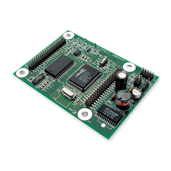
Summary of Contents for Digi Jackrabbit BL1800
- Page 1 Jackrabbit (BL1800) C-Programmable Single-Board Computer User’s Manual 019–0067 • 090515–J Downloaded from Elcodis.com electronic components distributor...
- Page 2 Trademarks Rabbit and Dynamic C are registered trademarks of Digi International Inc. Rabbit 2000 is a trademark of Digi International Inc. The latest revision of this manual is available on the Rabbit Web site, www.rabbit.com, for free, unregistered download.
-
Page 3: Table Of Contents
ABLE OF ONTENTS Chapter 1. Introduction 1.1 Features ..............................1 1.2 Development and Evaluation Tools......................2 1.3 How to Use This Manual ........................3 1.3.1 Additional Product Information ....................3 1.3.2 Online Documentation ........................3 1.4 CE Compliance .............................4 1.4.1 Design Guidelines .........................5 1.4.2 Interfacing the Jackrabbit to Other Devices..................5 Chapter 2. - Page 4 Chapter 4. Software Reference 4.1 An Overview of Dynamic C....................... 37 4.2 Sample Programs..........................39 4.2.1 DEMOJR1.C ..........................40 4.2.2 Other Sample Programs Illustrating Digital I/O................. 44 4.2.3 RS-232 Serial Communication Sample Programs ..............46 4.2.4 RS-485 Serial Communication Sample Program ............... 47 4.3 Cooperative Multitasking........................
-
Page 5: Chapter 1. Introduction
1. I NTRODUCTION The Jackrabbit is a high-performance, C-programmable single- ® board computer with a compact form factor. A Rabbit 2000 microprocessor operating at 29.5 MHz provides fast data pro- cessing. 1.1 Features • 29.5 MHz clock • 24 CMOS-compatible I/O •... -
Page 6: Development And Evaluation Tools
Three Jackrabbit models are available. Their standard features are summarized in Table 1. Table 1. Jackrabbit Features Model Features BL1800 Full-featured controller with switching voltage regulator. BL1800 with 14.74 MHz clock, 128K flash EPROM, linear voltage regulator, sinking outputs sink up to 200 mA, BL1810 sourcing output sources up to 100 mA, RS-232 serial ports rated for 1 kV ESD... -
Page 7: How To Use This Manual
1.3 How to Use This Manual This user’s manual is intended to give users detailed information on the Jackrabbit. It does not contain detailed information on the Dynamic C development environment or the Rabbit ® 2000 microprocessor. Most users will want more detailed information on some or all of these topics in order to put the Jackrabbit to effective use. -
Page 8: Ce Compliance
1.4 CE Compliance Equipment is generally divided into two classes. CLASS A CLASS B Digital equipment meant for light industrial use Digital equipment meant for home use Less restrictive emissions requirement: More restrictive emissions requirement: less than 40 dB µV/m at 10 m 30 dB µV/m at 10 m or 100 µV/m (40 dB relative to 1 µV/m) or 300 µV/m These limits apply over the range of 30–230 MHz. -
Page 9: Design Guidelines
digital I/O cables. Your results may vary, depending on your application, so additional shielding or filtering may be needed to maintain the Class B emission qualification. NOTE: If no ferrite absorbers are fitted, the Jackrabbit boards will still meet EN55022:1998 Class A requirements as long as the spectrum spreader is turned on. The spectrum spreader is on by default for Jackrabbit models BL1810 and BL1820. - Page 10 Jackrabbit (BL1800) Downloaded from Elcodis.com electronic components distributor...
-
Page 11: Chapter 2. Getting Started
2. G ETTING TARTED This chapter describes the Jackrabbit board in more detail, and explains how to set up and use the accompanying Prototyping Board. NOTE: This chapter (and this manual) assume that you have the Jackrabbit Development Kit. If you purchased a Jackrabbit board by itself, you will have to adapt the informa- tion in this chapter and elsewhere to your test and development setup. -
Page 12: Development Hardware Connections
2.2 Development Hardware Connections There are three steps to connecting the Prototyping Board for use with Dynamic C and the sample programs: 1. Attach the Jackrabbit to the Prototyping Board. 2. Connect the programming cable between the Jackrabbit and the workstation PC. 3. -
Page 13: Attach Jackrabbit To Prototyping Board
2.2.1 Attach Jackrabbit to Prototyping Board To attach the Jackrabbit board to the Prototyping Board, turn the Jackrabbit board over so that the battery is facing up. Plug the pins from headers J4 and J5 on the bottom side of the Jackrabbit board into the header sockets at J2 and J6 on the Prototyping Board as indicated in Figure 1. -
Page 14: Connect Programming Cable
2.2.2 Connect Programming Cable The programming cable connects the Jackrabbit to the PC running Dynamic C to down- load programs and to monitor the Jackrabbit during debugging. Connect the 10-pin connector of the programming cable labeled PROG to header J3 on the Jackrabbit board as shown in Figure 2. -
Page 15: Connect Power
2.2.3 Connect Power When all other connections have been made, you can connect power to the Jackrabbit. First, prepare the AC adapter for the country where it will be used by selecting the plug. The Jackrabbit Development Kit presently includes Canada/Japan/U.S., Australia/N.Z., U.K., and European style plugs. -
Page 16: Installing Dynamic C
2.3 Installing Dynamic C If you have not yet installed Dynamic C, do so now by inserting the Dynamic C CD from the Jackrabbit Development Kit in your PC’s CD-ROM drive. The CD will auto-install unless you have disabled auto-install on your PC. If the CD does not auto-install, click Start >... -
Page 17: Run A Sample Program
2.4 Run a Sample Program If you already have Dynamic C installed, you are now ready to test your programming connections by running a sample program. Start Dynamic C by double-clicking on the Dynamic C icon on your desktop or in your menu. -
Page 18: Where Do I Go From Here
2.5 Where Do I Go From Here? If everything appears to be working, we recommend the following sequence of action: 1. Run all of the sample programs described in Section 4.2 to get a basic familiarity with Dynamic C and the Jackrabbit’s capabilities. 2. -
Page 19: Chapter 3. Subsystems
3. S UBSYSTEMS Chapter 3 describes the principal subsystems and their use for the Jackrabbit. • Digital Inputs/Outputs • A/D Converter • D/A Converters • Serial Communication • Memory Figure 3 shows these Rabbit-based subsystems designed into the Jackrabbit. Digital BL1800 Inputs Programming... -
Page 20: Jackrabbit Pinouts
3.1 Jackrabbit Pinouts Figure 4 shows the pinout for headers J4 and J5, which carry the signals associated with the Jackrabbit subsystems. Legend Figure 4. Pinout for Jackrabbit Headers J4 and J5 3.1.1 Headers Standard Jackrabbit models are equipped with two 2 × 20 IDC headers (J4 and J5) with a 2 mm pitch. -
Page 21: Digital Inputs/Outputs
3.2 Digital Inputs/Outputs 3.2.1 Digital Inputs The Jackrabbit has six CMOS-level digital inputs, PB0–PB5, each of which is pulled up to +5 V as shown in Figure 5. The BL1820, which does not have RS-485, has one additional CMOS-level digital input, PC1. Rabbit 2000 ™... -
Page 22: Digital Outputs
3.2.2 Digital Outputs The Jackrabbit has four CMOS-level digital outputs, PB6–PB7, PCLK, and IOBEN. Four high-power outputs, HV0–HV3, are also available—HV0–HV2 can each sink up to 1 A (200 mA for the BL1810 and BL1820) at 30 V, and HV3 can source up to 500 mA (100 mA for the BL1810 and BL1820) at 30 V. - Page 23 3.2.2.1 Configurable High-Power Output (HV3) HV3, shown schematically in Figure 7, is factory-configured to be a sourcing output. Figure 7. Configurable High-Current Output When used as a sourcing output, HV3 is switched to K when PE3 on the Rabbit 2000 goes high, and the two transistors shown in Figure 7 are turned on.
-
Page 24: Bidirectional I/O
HV3 can also be reconfigured as a sinking output. To do so, remove the 0 Ω surface- mounted resistor R56, and solder on a 0 Ω surface-mounted resistor or jumper wire at R55. If you plan to drive inductive loads, add a diode at D21. Figure 8 shows the location of these components. -
Page 25: A/D Converter
3.3 A/D Converter The analog-to-digital (A/D) converter, shown in Figure 9, compares the DA0 voltage to AD0, the voltage presented to the converter. DA0 therefore cannot be used for the digital- to-analog (D/A) converter when the A/D converter is being used. Figure 9. - Page 26 There is a 10 kΩ resistor, R31, connected between Vcc and AD0. This resistor should pro- vide an appropriate voltage divider bias for a variety of common thermistors so that they can be connected directly between AD0 and ground. The A/D converter load is the 10 kΩ resistor connected to Vcc.
-
Page 27: D/A Converters
D/A conversion when the A/D converter is being used. Pulse-width modulation (PWM) is used for the D/A conversion. This means that the digi- tal signal, which is either 0 V or 5 V, is a train of pulses. This means that if the signal is taken to be usually at 0 V (or ground), there will be 5 V pulses. -
Page 28: Da1
It is very easy to do pulse-width modulation with the Rabbit 2000 microprocessor because of the chip’s architecture. 3.4.1 DA1 The op amp supporting DA1 converts pulse-width modulated signals to an analog voltage between 0 V and 5 V. A digital signal that varies with time is fed from PD4. The resolution of the DA1 output depends on the smallest increment of time to change the on/off time (the time between 5 V and 0 V). - Page 29 either a 0% or a 100% duty cycle. The duty cycle is programmed as the high-time count of 1024 total counts of the Rabbit 2000’s timer B. Thus, 256 counts would be 25% of 1024 counts, and corresponds to a 25% duty cycle. Table 2 lists typical DA1 voltages measured for various duty cycle values with a load larger than 1 MΩ.
-
Page 30: Da0
3.4.2 DA0 The op amp supporting DA0 translates a 12%–88% duty cycle to an analog voltage range of 0 V to 3 V. The software operates only within this duty cycle; a duty cycle less than 12% is rounded down to 0%, and any duty cycle above 88% is rounded up to 100%. DA0 uses a voltage divider that consists of R21 and R27 and a gain-offset circuit that con- sists of R26 and R29 to achieve the output range of 0 V to 3 V within the software duty cycle. - Page 31 The resolution of the DA0 output depends on the smallest increment of time to change the on/off time (the time between 5 V and 0 V). The Jackrabbit uses the Rabbit 2000’s Port D control registers to clock out the signal at a timer timeout. The timer used is timer B. Timer B has 10 bits of resolution so that the voltage can be varied in 1/1024 increments.
-
Page 32: Serial Communication
3.5 Serial Communication The Jackrabbit has two RS-232 (3-wire) serial channels, one RS-485 serial channel, and one synchronous CMOS serial channel. 3.5.1 RS-232 The Jackrabbit’s two RS-232 serial channels are connected to an RS-232 transceiver, U4, an industry-standard MAX232 chip. U4 provides the voltage output, slew rate, and input voltage immunity required to meet the RS-232 serial communication protocol. - Page 33 Figure 11. Multidrop Jackrabbit Network User’s Manual Downloaded from Elcodis.com electronic components distributor...
-
Page 34: Programming Port
The Jackrabbit comes with a 220 Ω termination resistor and 681 Ω bias resistors already installed, as shown in Figure 12. bias termination bias Figure 12. RS-485 Termination and Bias Resistors The load these bias and termination resistors present to the RS-485 transceiver (U6) limits the number of Jackrabbits in a multidrop network to one master and nine slaves, unless the bias and termination resistors are removed. - Page 35 In addition to Serial Port A, the Rabbit 2000 startup-mode (SMODE0, SMODE1), status, and reset pins are available on the serial programming port. The two startup mode pins determine what happens after a reset—the Rabbit 2000 is either cold-booted or the program begins executing at address 0x0000. These two SMODE pins can be used as general inputs once the cold boot is complete.
-
Page 36: Programming Cable
3.6 Programming Cable The programming cable is used to connect the Jackrabbit’s programming port to a PC serial COM port. The programming cable converts the RS-232 voltage levels used by the PC serial port to the TTL voltage levels used by the Rabbit 2000. When the PROG connector on the programming cable is connected to the Jackrabbit’s... -
Page 37: Memory
3.7 Memory 3.7.1 SRAM The Jackrabbit is designed to accept 32K to 512K of SRAM packaged in an SOIC case. Standard Jackrabbit models come with 128K of SRAM. A factory-installed option for 512K of SRAM is available. Figure 14 shows the locations and the jumper settings for the jump- ers at JP1 used to set the SRAM size. -
Page 38: Other Hardware
3.8 Other Hardware 3.8.1 External Interrupts Jackrabbit boards that carry the CE mark have external interrupts available on digital inputs PE4 and PE5. 3.8.2 Clock Doubler Jackrabbit BL1810 and BL1820 models take advantage of the Rabbit 2000 microproces- sor’s internal clock doubler. A built-in clock doubler allows half-frequency crystals to be used to reduce radiated emissions. -
Page 39: Spectrum Spreader
Jackrabbit BL1800 models only, you will need at least one wait state for both the flash memory and the RAM. The strong spectrum-spreading setting is not needed for any Jackrabbit board. - Page 40 Jackrabbit (BL1800) Downloaded from Elcodis.com electronic components distributor...
-
Page 41: Chapter 4. Software Reference
4. S OFTWARE EFERENCE To develop and debug programs for the Jackrabbit (and for all other Rabbit hardware), you must install and use Dynamic C. It runs on an IBM-compatible PC and is designed for use with Rabbit-based single-board computers and other devices based on the Rabbit microprocessor. - Page 42 Dynamic C has a number of standard features: • Full-feature source and/or assembly-level debugger, no in-circuit emulator required. • Royalty-free TCP/IP stack with source code and most common protocols. • Hundreds of functions in source-code libraries and sample programs: Exceptionally fast support for floating-point arithmetic and transcendental functions. RS-232 and RS-485 serial communication.
-
Page 43: Sample Programs
4.2 Sample Programs Sample programs are provided in the Dynamic C folder. S A M P L E S The various folders contain specific sample programs that illustrate the use of the corre- sponding Dynamic C libraries. For example, the sample program demonstrates PONG.C the output to the Dynamic C... -
Page 44: Demojr1.C
4.2.1 DEMOJR1.C This sample program can be used to illustrate some of the functions of Dynamic C. First, open the file , which is in the folder. The program DEMOJR1.C SAMPLES/JACKRAB will appear in a window, as shown in Figure 15 below (minus some comments). Use the mouse to place the cursor on the function name WrPortI in the program and type <Ctrl-H>... - Page 45 • The programming cable must be connected to the Jackrabbit board. (The colored wire on the programming cable is closest to pin 1 on header J3 on the Jackrabbit board, as shown in Figure 2.) The other end of the programming cable must be connected to the PC serial port.
- Page 46 Editing the Program Click on the Edit box on the task bar. This will set Dynamic C into the edit mode so that you can change the program. Use the choice on the menu to save the file Save as File with a new name so as not to change the demo program.
- Page 47 • Setting break points. The key is used to turn on or turn off (toggle) a break point at the cursor position if the program has already been compiled. You can set a break point if the program is paused at a break point. You can also set a break point in a program that is running at full speed.
-
Page 48: Other Sample Programs Illustrating Digital I/O
4.2.2 Other Sample Programs Illustrating Digital I/O —repeatedly flashes LED DS3 (which is controlled by PA2) on the Proto- • DEMOJR2.C typing Board. This sample program also illustrates the use of the function to allow runwatch() Dynamic C to update watch expressions while running. To test this: 1. - Page 49 Before running the sample program, you will need an LCD based on the LCD_DEMO.C HD44780 (or an equivalent) controller. —demonstrates a 4-bit interface to an LCD based on the HD44780 (or an • LCD_DEMO.C equivalent) controller. Connect the LCD to Parallel Port A. Jackrabbit PA0—LCD DB4 Prototyping Board...
-
Page 50: Rs-232 Serial Communication Sample Programs
4.2.3 RS-232 Serial Communication Sample Programs —This program demonstrates hardware flow control by config- • JR_FLOWCONTROL.C uring Serial Port C (PC3/PC2) for CTS/RTS with serial data coming from TxB at 115,200 bps. One character at a time is received and is displayed in the window. -
Page 51: Rs-485 Serial Communication Sample Program
4.2.4 RS-485 Serial Communication Sample Program The following sample program illustrates the use of the RS-485 serial drivers. The sample program shows a byte being transmitted, and then the RS-485 transceiver waits for a reply. #define DINBUFSIZE #define DOUTBUFSIZE 15 void main( void ){ int nEcho,nReply;... -
Page 52: Cooperative Multitasking
4.3 Cooperative Multitasking Cooperative multitasking is a convenient way to perform several different tasks at the same time. An example would be to step a machine through a sequence of steps and at the same time independently carry on a dialog with the operator via a human interface. Coop- erative multitasking differs from a different approach called preemptive multitasking. - Page 53 int vswitch; // state of virtual switch controlled by button main(){ // begin main program // set up parallel port A as output WrPortI(SPCR,NULL,0x84); WrPortI(PADR,&PADRShadow,0xff); // turn off all LEDs vswitch=0; // initialize virtual switch off (1) while (1) { // Endless loop BigLoopTop();...
-
Page 54: Advantages Of Cooperative Multitasking
used to collect some operations that are helpful to do once on every pass through the loop. Place the cursor on this function name and hit to learn more. <Ctrl-H> BigLoopTop() The statement at (3) waits for a time delay, in this case 200 ms. The costatement is being executed on each pass through the big loop. -
Page 55: Jackrabbit Function Calls
4.4 Jackrabbit Function Calls 4.4.1 I/O Drivers The Jackrabbit contains four high-power digital output channels, two D/A converter out- put channels, and one A/D converter input channel. These I/O channels can be accessed using the functions found in the library. JRIO.LIB 4.4.1.1 Initialization The function... - Page 56 void digOut(int channel, int value); sets the state of a digital output bit. jrioInit must be called first. channel is the output channel number (0-3 on the Jackrabbit). value is the output value (0 or 1). void digOn(int channel); sets the state of a digital output bit to on (1). jrioInit must be called first.
- Page 57 Table 5. Typical Analog Output Voltages Corresponding to Values in anaOut Function Channel 1024 PWM_MIN PWM_MAX 0.08 V 0.08 V 2.875 V 3.4 V 0.004 V 0.63 V 3.6 V 3.6 V The output value is set using the following function. void anaOut(int channel, int value);...
- Page 58 – -------------------------------------------------------------------- - PWM_MAX0 PWM_MIN – × voltage m value 4.4.1.4 Analog Input The analog input channel on the Jackrabbit (AD0 on header J5) works by varying analog output channel DA0 until its voltage matches the input voltage on AD0. DA0 obviously cannot be used while an input voltage is being measured, although channel DA0 is still available.
-
Page 59: Serial Communication Drivers
4.4.2 Serial Communication Drivers Library files included with Dynamic C provide a full range of serial communications sup- port. The library provides a set of circular-buffer-based serial functions. The RS232.LIB library provides packet-based serial functions where packets can be delim- PACKET.LIB ited by the 9th bit, by transmission gaps, or with user-defined special characters. -
Page 60: Upgrading Dynamic C
4.5 Upgrading Dynamic C 4.5.1 Patches and Bug Fixes Dynamic C patches that focus on bug fixes are available from time to time. Check the Web site www.rabbit.com/support/ for the latest patches, workarounds, and bug fixes. The default installation of a patch or bug fix is to install the file in a directory (folder) dif- ferent from that of the original Dynamic C installation. -
Page 61: Appendix A. Specifications
A. S PPENDIX PECIFICATIONS Appendix A provides the specifications for the Jackrabbit. User’s Manual Downloaded from Elcodis.com electronic components distributor... -
Page 62: Electrical And Mechanical Specifications
A.1 Electrical and Mechanical Specifications Figure A-1 shows the mechanical dimensions for the Jackrabbit. Please refer to the Jackrabbit footprint diagram later in this appendix for precise header locations. Figure A-1. Jackrabbit Dimensions NOTE: All measurements are in inches followed by millimeters enclosed in parentheses. All dimensions have a manufacturing tolerance of ±0.01"... - Page 63 Table A-1 lists the electrical, mechanical, and environmental specifications for the Jackrabbit boards. Table A-1. Jackrabbit Board Specifications Parameter BL1800 BL1810 BL1820 Microprocessor Rabbit 2000 @ 29.5 MHz Rabbit 2000 @ 14.74 MHz 256K 128K Flash EPROM (supports 128K–512K) (supports 128K–512K) 128K SRAM (supports 32K–512K)
-
Page 64: Exclusion Zone
A.1.1 Exclusion Zone It is recommended that you allow for “exclusion zones” around the Jackrabbit when the Jackrabbit is incorporated into an assembly that includes other components. These “exclu- sion zones” that you keep free of other components and boards will allow for sufficient air flow, and will help to minimize any electrical or EMI interference between adjacent boards. -
Page 65: Headers
A.1.2 Headers The Jackrabbit has 0.1" IDC headers at J1 (1 × 3) and J2 (2 × 2) for the power supply and an external battery connection. There are 2 mm IDC headers at J3 (2 × 5 programming port) and at J4 and J5 (2 × 20 Rabbit subsystems) for physical connection to other boards or ribbon cables. -
Page 66: Jumper Configurations
A.2 Jumper Configurations Figure A-4 shows the header and jumper locations used to configure the various Jackrabbit options. Top Side Bottom Side Figure A-4. Location of Jackrabbit Configurable Positions Jackrabbit (BL1800) Downloaded from Elcodis.com electronic components distributor... - Page 67 Table A-2 lists the configuration options. 0 Ω surface mount resistors are used for all the header positions. Table A-2. Jackrabbit Jumper Configurations Factory Header Description Pins Connected Default n.c. × SRAM Size 1–2 128K 2–3 512K × 1–2 128K/256K Flash Memory Size 2–3 512K ×...
-
Page 68: Conformal Coating
A.3 Conformal Coating The areas around the crystal oscillator and the battery backup circuit on the Jackrabbit have had the Dow Corning silicone-based 1-2620 conformal coating applied. The confor- mally coated areas are shown in Figure A-5. The conformal coating protects these high- impedance circuits from the effects of moisture and contaminants over time, and helps to maintain the accuracy of the real-time clock. -
Page 69: Use Of Rabbit 2000 Parallel Ports
A.4 Use of Rabbit 2000 Parallel Ports Figure A-6 shows the use of the Rabbit 2000 parallel ports. The Jackrabbit has 27 general- purpose digital inputs/outputs available on headers J4 and J5—15 are bidirectional (one of which is used by the RS-485 chip on BL1800 and BL1810 models), seven are inputs only (one of which is used by the RS-485 chip on BL1800 and BL1810 models), and five are outputs only (one of which is used by the RS-485 chip on BL1800 and BL1810 models), as shown in Figure A-6. - Page 70 The ports on the Rabbit 2000 microprocessor used in the Jackrabbit are configurable, and so the factory defaults can be reconfigured. Table A-3 lists the Rabbit 2000 factory defaults and the alternate configurations. Table A-3. Jackrabbit Pinout Configurations Rabbit 2000 Alternate Use Jackrabbit Use Factory Default...
- Page 71 Table A-3. Jackrabbit Pinout Configurations (continued) Rabbit 2000 Alternate Use Jackrabbit Use Factory Default Connected to control Connected to control Bitwise or parallel programmable I/O, can be driven or open- Connected to control ATXB output drain output Connected to RS-485 IC ARXB input data enable input ATXA output...
- Page 72 Jackrabbit (BL1800) Downloaded from Elcodis.com electronic components distributor...
-
Page 73: Appendix B. Prototyping Board
B. P PPENDIX ROTOTYPING OARD Appendix B describes the features and accessories of the Proto- typing Board, and explains the use of the Prototyping Board to demonstrate the Jackrabbit and to build prototypes of your own circuits. User’s Manual Downloaded from Elcodis.com electronic components distributor... -
Page 74: Prototyping Board Overview
B.1 Prototyping Board Overview The Prototyping Board included in the Development Kit makes it easy to connect a Jack- rabbit board to a power supply and a PC workstation for development. It also provides some basic I/O peripherals (switches and LEDs), as well as a prototyping area for more advanced hardware development. -
Page 75: Prototyping Board Features
B.1.1 Prototyping Board Features Power LED —The power LED lights whenever power is connected to the Prototyping • Board. Reset Switch —A momentary-contact, normally open switch is connected directly to the • Jackrabbit’s /RESET_IN pin. Pressing the switch forces a hardware reset of the system. —Four momentary-contact, normally open switches are con- •... -
Page 76: Mechanical Dimensions And Layout
B.2 Mechanical Dimensions and Layout Figure B-2 shows the mechanical dimensions and layout for the Jackrabbit Prototyping Board. Top Side Bottom Side Figure B-2. Jackrabbit Prototyping Board Jackrabbit (BL1800) Downloaded from Elcodis.com electronic components distributor... -
Page 77: Using The Prototyping Board
B.3 Using the Prototyping Board The Prototyping Board is actually both a demonstration board and a prototyping board. As a demonstration board, it can be used to demonstrate the functionality of the Jackrabbit right out of the box without any modifications to either board. There are no jumpers or dip switches to configure or misconfigure on the Prototyping Board so that the initial setup is very straightforward. -
Page 78: Demonstration Board
B.3.1 Demonstration Board A relay, a thermistor, four additional LEDs, and a serial cable are included in a bag of parts to further allow exploration of the Jackrabbit‘s operation. The SPDT relay handles 120 V at 5 A with a 12 V activating coil. The layout to accept this relay is included on the top side of the Prototyping Board. - Page 79 The thermistor has a nominal room-temperature resistance of about 10 kΩ, which drops to about 6 kΩ at 40°C. Once you solder the thermistor onto the RT1 pads (see Figure B-5) on the Prototyping Board, the A/D converter readings on AD0 will change with temperature.
-
Page 80: Prototyping Board
B.3.2 Prototyping Board To maximize the availability of Jackrabbit resources, the demonstration hardware (LEDs, switches, potentiometer, buzzer) on the Prototyping Board may be disconnected. This is done by cutting the traces seen between and within the silk-screen outline of headers JP1 and JP2 on the Prototyping Board. - Page 81 Once the LEDs, resistors, and switches are disconnected as described above, the user has a Jackrabbit board with connection points conveniently brought out to labeled points at headers J3 and J7 on the Prototyping Board. Small to medium circuits can be prototyped using point- to-point wiring with 20 to 30 AWG wire between the prototyping area and the holes at loca- tions J3 and J7.
- Page 82 Jackrabbit (BL1800) Downloaded from Elcodis.com electronic components distributor...
-
Page 83: Appendix C. Power Management
C. P PPENDIX OWER ANAGEMENT C.1 Power Supplies Power is supplied to the Jackrabbit board from an external source through either header J1 or header J4. J1 is a 3-pin straight header with a pitch of 0.1". V is on pin 2 between ground on pins 1 and 3. - Page 84 The linear voltage regulator is simply a fixed-voltage regulator with a ±5% voltage output tolerance as the temperature changes. The regulator has a small heat sink, which increases the maximum external input voltage. Higher external input voltages increase the voltage dropped by the regulator.
- Page 85 The switching voltage regulator is used when there is a need for an additional range in the external input voltage or when lower power consumption is desired. The input voltage range is from 8 V to 40 V. Figure C-3 shows typical power operating curves for both the linear regulator (BL1810 and BL1820) and the switching regulator (BL1800) for a nonloaded Jackrabbit operating at 14.74 MHz with the programming cable connected.
-
Page 86: Batteries And External Battery Connections
C.2 Batteries and External Battery Connections The soldered-in 950 mA·h lithium coin cell provides power to the real-time clock and SRAM when external power is removed from the circuit. This allows the Jackrabbit to continue to keep track of time and preserves the SRAM memory contents. The drain on the battery is typically less than 20 µA when there is no external power applied. -
Page 87: Battery Backup Circuit
C.2.1 Battery Backup Circuit Figure C-5 shows the Jackrabbit battery backup circuitry. Figure C-5. Jackrabbit Battery Backup Circuit Resistor R12, shown in Figure C-5, is typically not stuffed on the Jackrabbit board. VRAM and Vcc are equal when power is supplied to the Jackrabbit. R13 prevents any cat- astrophic failure of Q1 from allowing unlimited current to enter the soldered-in battery. -
Page 88: Power To Vram Switch
The battery-backup circuit serves two purposes: • It reduces the battery voltage to the real-time clock, thereby reducing the current con- sumed by the real-time clock and lengthening the battery life. • It ensures that current can flow only out of the battery to prevent charging the battery. C.2.2 Power to VRAM Switch The VRAM switch, shown in Figure C-6, allows the soldered-in battery to provide power when the external power goes off. -
Page 89: Chip Select Circuit
C.3 Chip Select Circuit Figure C-7 shows a schematic of the chip select circuit. Figure C-7. Chip Select Circuit The current drain on the battery in a battery-backed circuit must be kept at a minimum. When the Jackrabbit board is not powered, the battery keeps the SRAM memory contents and the real-time clock (RTC) going. - Page 90 Transistors Q20 and Q21 are of opposite polarity so that a rail-to-rail voltages can be passed. When the /CS1 voltage is low, Q20 will conduct. When the /CS1 voltage is high, Q21 will conduct. It takes time for the transistors to turn on, creating a propagation delay. This delay is typically very small, about 10 ns to 15ns.
-
Page 91: Index
NDEX digital inputs switching threshold ... 17 A/D converter ....21, 22 Jackrabbit digital outputs additional information dimensions ......58 function calls online documentation ..3 electrical specifications ..59 digOff ......52 analog input jumper configurations ..62, 63 digOn ...... - Page 92 Prototyping Board (continued) serial communication ....28 pinout .........77 function calls prototyping area ....77 Jr485Init ......55 thermistor ......75 Jr485Rx ......55 Jr485Tx ......55 programming port ....30 RS-232 .......28 Rabbit 2000 parallel ports 65, 66 RS-485 .......28 real-time clock RS-485 network ....29 how to set ......14 RS-485 termination and bias reset ........11 resistors ......30...
-
Page 93: Schematics
CHEMATICS 090-0092 Jackrabbit Schematic www.rabbit.com/documentation/schemat/090-0092.pdf 090-0088 Jackrabbit Prototyping Board Schematic www.rabbit.com/documentation/schemat/090-0088.pdf 090-0128 Programming Cable Schematic www.rabbit.com/documentation/schemat/090-0128.pdf You may use the URL information provided above to access the latest schematics directly. User’s Manual Downloaded from Elcodis.com electronic components distributor... - Page 94 Downloaded from Elcodis.com electronic components distributor...
Need help?
Do you have a question about the Jackrabbit BL1800 and is the answer not in the manual?
Questions and answers