Harman Kardon AVR145 Service Manual
5 x 40w 5.1 channel a/v receiver
Hide thumbs
Also See for AVR145:
- Brochure & specs (52 pages) ,
- Owner's manual (50 pages) ,
- Settings manual (3 pages)
Table of Contents
Advertisement
harman/kardon
5 X 40W 5.1 CHANNEL A/V RECEIVER
Esd Warning.....................................2
Leakage Testing...............................3
Basic Specifications.......................4
Packaging........................................5
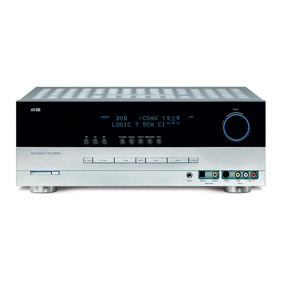
Front Panel Controls.....................6
Rear Panel Connections................8
Remote Control Functions..........10
Connections/Installation.............13
Operation.......................................22
Troubleshooting Guide.................26
REMOTE & PROCESSOR RESETS..........26
AVR145
SERVICE MANUAL
CONTENTS
harman/kardon, Inc.
250 Crossways Park Dr.
Woodbury, New York 11797
Disassembly.....................................27
Unit Exploded View..........................31
Exploded View Parts List...............32
Amp Bias Adjustment......................33
Block Diagram................................34
Pcb Drawings.................................35
ELECTRICAL PARTS LIST.....................42
Semiconductor Pinouts................73
Schematics....................................144
Wiring Diagram..............................151
Rev 0 1/2007
Advertisement
Table of Contents

Related Manuals for Harman Kardon AVR145


Summary of Contents for Harman Kardon AVR145
- Page 1 AVR145 5 X 40W 5.1 CHANNEL A/V RECEIVER SERVICE MANUAL CONTENTS ESD WARNING……………………………….2 DISASSEMBLY……………………………….27 LEAKAGE TESTING……………….…..…..3 UNIT EXPLODED VIEW…………..…….…..31 BASIC SPECIFICATIONS…………………..4 EXPLODED VIEW PARTS LIST……………32 PACKAGING…………………………….……5 AMP BIAS ADJUSTMENT……………….…33 FRONT PANEL CONTROLS………..…..…..6 BLOCK DIAGRAM…………………………..34 REAR PANEL CONNECTIONS………….…8 PCB DRAWINGS……………………………35 REMOTE CONTROL FUNCTIONS……….10...
- Page 2 AVR145 Some semiconductor (solid state) devices can be damaged easily by static electricity. Such components commonly are called Electrostatically Sensitive (ES) Devices. Examples of typical ES devices are integrated circuits and some field effect transistors and semiconductor "chip" components.
- Page 3 AVR145 SAFETY PRECAUTIONS The following check should be performed for the continued protection of the customer and service technician. LEAKAGE CURRENT CHECK Measure leakage current to a known earth ground (water pipe, conduit, etc.) by connecting a leakage current tester...
- Page 4 All features and specifications are subject to change without notice. Transient Intermodulation Distortion (TIM) Unmeasurable Harman Kardon, Harman International, Designed to Entertain and Logic 7 are trademarks of Harman International Slew Rate 40V/µsec Industries, Incorporated, registered in the United States and/or other countries.
- Page 5 AVR145 AVR 145 DOOR KIT FRONT COVER "A", SILVER FRONT COVER "B", SILVER...
- Page 6 AVR145 FRONT-PANEL CONTROLS Main Power Switch: Analog Audio, Video and Digital Audio Inputs: This is a mechanical switch that turns the Connect a power supply on or off. It is usually left pressed in (On position) at all source component that will only be used temporarily to these jacks, times, and cannot be turned on using the remote control.
- Page 7 AVR145 Source Digital Input Message Display Speaker Size Tone Mode Indicators Select Setup Speaker/Channel Channel Level Surround Mode Indicators Volume Navigation Delay Input Indicators Adjust Headphone Digital Power Surround Tuning Preset Stations Analog Audio Jack Audio Inputs Indicator Mode...
- Page 8 These jacks may be used to con- This specialized connector may be used with nect your VCR or another recorder. your personal computer in case Harman Kardon offers a software upgrade for the receiver at some time in the future. Composite and S-Video Monitor Outputs:...
- Page 9 AVR145 Video 2 Video 1 Video Monitor Component Video Coaxial Digital RS-232 AC Power Audio Inputs Serial Port FM Antenna Inputs Inputs Outputs Monitor Outputs Cord (1 & 2) Video 1 DVD A/V Component Video RS-232 The Bridge/ RS-232...
-
Page 10: Remote Control Functions
AVR145 REMOTE CONTROL FUNCTIONS The AVR 145 remote is capable of controlling nine devices, including Mute Button: Press this button to mute the AVR 145’s speaker and the AVR itself and an iPod docked in the optional The Bridge accessory. - Page 11 AVR145 REMOTE CONTROL FUNCTIONS Speaker Setup: Surround Mode Selectors: Press this button to configure speaker sizes, that is, Press any of these buttons to select the frequency-range capability of each speaker. Usually this is done a type of surround sound (e.g., multichannel) mode. Choose from the using the on-screen menu system, as described in the Getting Started Dolby modes, DTS modes, Logic 7 modes or Stereo modes.
- Page 12 AVR145 EzSet Microphone IR Transmitter Lens Power On Mute Program/EzSet Indicator Power Off Input Selectors AVR Selector 6-Channel Input Selector AM/FM Bridge EzSet (SPL) /DMP Selector Test Tone TV/Video Sleep Volume Control DSP Surround Not Used On-Screen Display Speaker Setup...
- Page 13 AVR145 CONNECTIONS There are different types of audio and video connections used to con- Bare wire cables are installed as follows: nect the receiver to the speakers and video display, and to connect 1. Unscrew the terminal cap until the pass-through hole in the collar is the source devices to the receiver.
-
Page 14: Audio Connections
Figure 8 – The Bridge Coaxial digital Coaxial Harman Kardon receivers also include a proprietary, dedicated audio audio cable connection called “The Bridge/DMP”. If you own an iPod with a dock Figure 4 – Coaxial Digital Audio connector, you may separately purchase The Bridge and connect it to The Bridge/DMP port on the receiver. - Page 15 RS-232 Serial Port The RS-232 serial port on the AVR 145 is used only for data. If Harman Kardon releases a software upgrade for the receiver’s operating system at some time in the future, the upgrade may be downloaded to the AVR using this port. Complete instructions will be provided at...
- Page 16 AVR145 INSTALLATION You are now ready to connect your various components to your receiver. Step Three – Connect the Antennas Before beginning, make sure that all components, including the AVR 145, Connect the FM and AM antennas to their terminals.
- Page 17 AVR145 INSTALLATION We recommend connecting your various sources using the connections shown in Table 2 below in order to simplify programming your receiver NOTE: It’s possible for a source to use none of the connections and remote control. However, you may connect any device to any named for that source.
- Page 18 AVR145 INSTALLATION STEPS NOTE: It isn’t possible to make recordings using component The DVD source is used for a DVD player. If you have a more advanced video connections. Keep this in mind as you connect other multichannel device, such as a Blu-ray Disc or HD-DVD player, connect source devices that you may wish to make recordings from.
- Page 19 Figure 27 – S-Video and Composite Video Monitor Outputs Bridge With Harman Kardon’s optional The Bridge, you can listen to audio Consult the manual for your TV to make sure you understand how to stored on your iPod (not included), use your AVR 145 remote select each video input.
- Page 20 Cable, Satellite docked in The Bridge are preprogrammed, and the codes for many Video 3 Harman Kardon DVD and CD players are also preprogrammed. If you have other source devices in your system, follow these steps to pro- CD, CDR gram the correct codes into the remote.
- Page 21 NOTE: The AVR 145 remote is preprogrammed to operate the grammed to operate that device. In order to control the receiver, transport controls of Harman Kardon DVD players when the AVR you will need to press the AVR button to return the remote to or the Video 2 (cable/satellite) or Video 3 (TV) source is selected.
-
Page 22: Operation
AVR145 OPERATION Now that you have installed your system components and completed at To turn the receiver off, press either the Standby/On Switch on the front least a basic configuration of your receiver, you are ready to begin panel, or press the AVR Button and the OFF Button on the remote. -
Page 23: Mute Function
AVR145 OPERATION Remember that the AVR 145 is designed to reproduce audio with a BACK TO MASTER MENU line if you wish to make other changes using minimum amount of distortion. This clarity may lead you to think that the menu system. -
Page 24: Using The Tuner
AVR145 OPERATION INDEPENDENT, the AVR 145 will change the speaker size configuration source, it will be selected. If your device is not using component video, to the one you programmed for the source. If you selected a surround make sure that other devices connected to the component video inputs mode for the source, the AVR 145 will switch to that mode. - Page 25 AVR145 OPERATION Radio stations may be selected in one of four ways: NOTES: 1. If you know the frequency number, enter it directly by first pressing 1. Analog audio signals are not converted to digital form, and the Direct Button on the remote, and then using the Numeric Keys.
-
Page 26: Troubleshooting Guide
RESET message appears in the display. If the receiver still does not function correctly after a processor reset, contact an authorized Harman Kardon service center for assistance. Service centers may be located by visiting our Web site at www.harmankardon.com. -
Page 27: Disassembly
DISASSEMBLY AVR145 harman/kardon AVR145 1. Removing the Top Cabinet 3. Removing the Rear Panel Remove the Screws Remove the Screws 16 17 21 22 4. Removing the Main PCB Remove the Screws 2. Removing the Front Panel Remove the Screws... - Page 28 AVR145 AVR145 DISASSEMBLY PROCEDURE 1 TOP-CABINET (21) REMOVAL 1. Remove 13 screws (S1,S7) and then remove the Top-cabinet. FRONT PANEL ASS’Y REMOVAL 1. Remove the Top-cabinet, referring to the previous step 1. 2. Disconnect the card cable between connector (CN72-17p) on the FIP PCB (37-1) and connector (CN72) on the Input PCB (39-1).
- Page 29 AVR145 8 TUNER MODULE (42) REMOVAL 1. Remove the Top-cabinet, referring to the previous step 1. 2. Disconnect the card cable between connector (CON1-13p) on the Tuner module (42) and connector (CN13) on Input PCB (39-1). 3. Remove 2 screws (S8) and then remove the Tuner Module (42).
- Page 30 AVR145 14 MAIN PCB ASS’Y (38-1) REMOVAL 1. Remove the Top-cabinet, referring to the previous step 1. 2. Remove the Tuner module (42), referring to the previous step8. 3. Remove the Video PCB (41) referring to the previous step9.
- Page 31 AVR145 AVR145 EXPLODED VIEW 37-7 39-2 40-1 40-3 40-4 39-1 40-5 40-2 38-1 38-2 40-2 DESCRIPTION PARTS NO. Q,ty Weright ORNAMENT,VOLUME CGU1A318Z CAP,VOLUME CGX1A338MBC63 HOLDER,VOLUME CMH1A214 INDICATOR,VOLUME CGL1A222 WINDOW ASS'Y CGUAVR145 WINDOW,FIP CGU1A399Z BADGE,MODEL CGB1A168Z SHEET,VOLUME CMZ2A090 FILTER,FIP CMZ1A088...
- Page 32 AVR145...
- Page 33 AVR145...
- Page 34 AVR145...
- Page 35 AVR145...
- Page 36 AVR145...
- Page 37 AVR145...
- Page 38 AVR145...
- Page 39 AVR145...
- Page 40 AVR145...
- Page 41 AVR145...
- Page 42 AVR145 AVR145 Electrical Parts List Ref. Designator Part Number Description FRONT PCB ASSY CUP11910-1 Capacitors C714 HCBS1H151KBT CAP , CERAMIC 150UF 50V K C716 CCEA1AH331T CAP , ELECT 330UF 10V C723 HCBS1H104ZFT CAP , CERAMIC 0.1UF 50V Z C728...
- Page 43 AVR145 Ref. Designator Part Number Description FRONT PCB ASSY CUP11910-1 Miscellaneous CMC3A111 PLATE , EARTH PLATE L702 HLQ02C100KT COIL , AXAIL COIL FIP1 HFLHCA18ML03 F.I.P F.I.P CN72 CJP17GA193ZY WAFER, CARD CABLE (SMD) WAFER CN89 CJP04GB46ZY WAFER WAFER BN81 CWB2C908200BM...
- Page 44 AVR145 Ref. Designator Part Number Description PCB , FRONT PANEL KEY CUP11910-2 R764 CRD20TF5601T RES ,CARBON(5.6K/F) 5.6K/1/5W/F R765 CRD20TF7501T RES , CARBON (7.5K/F) 7.5K/1/5W/F R766 CRD20TF1001T RES , CARBON 1K /1/5W /F R767 CRD20TF1501T RES , CARBON 1.5K /1/5W /F...
- Page 45 AVR145 Ref. Designator Part Number Description PCB , VR JACK CUP11910-6 R871 CRD20TJ104T RES , CARBON 100K OHM 1/5W J R872 CRD20TJ104T RES , CARBON 100K OHM 1/5W J R873 CRD20TJ471T RES , CARBON 470 OHM 1/5W J R874...
- Page 46 AVR145 Ref. Designator Part Number Description PCB , PHONE JACK CUP11910-5 R897 CRD20TJ101T RES , CARBON 100 OHM 1/5W J R898 CRD20TJ101T RES , CARBON 100 OHM 1/5W J R899 CRD20TJ104T RES , CARBON 100K OHM 1/5W J R900...
- Page 47 AVR145 Ref. Designator Part Number Description MAIN PCB/HEATSINK (CUP11911Z) C601 CCCT1H120JC CAP , CERAMIC 12PF 50V C602 CCCT1H120JC CAP , CERAMIC 12PF 50V C603 CCCT1H120JC CAP , CERAMIC 12PF 50V C604 CCCT1H120JC CAP , CERAMIC 12PF 50V C605 CCCT1H120JC...
- Page 48 AVR145 Ref. Designator Part Number Description MAIN PCB/HEATSINK (CUP11911Z) Semiconductors D501 CVD1SS133MT DIODE 1SS133 D502 CVD1SS133MT DIODE 1SS133 D503 CVD1SS133MT DIODE 1SS133 D504 CVD1SS133MT DIODE 1SS133 D505 CVD1SS133MT DIODE 1SS133 D581 CVD1SS133MT DIODE 1SS133 D582 CVD1SS133MT DIODE 1SS133 D583...
- Page 49 AVR145 Ref. Designator Part Number Description MAIN PCB/HEATSINK (CUP11911Z) Q602 HVTKTA1268GRT TRANSISTOR PNP KTA1268GR Q603 HVTKTA1268GRT TRANSISTOR PNP KTA1268GR Q604 HVTKTA1268GRT TRANSISTOR PNP KTA1268GR Q605 HVTKTA1268GRT TRANSISTOR PNP KTA1268GR Q681 HVTKSC2785YT TRANSISTOR NPN KSC2785Y Q682 HVTKSC2785YT TRANSISTOR NPN KSC2785Y...
- Page 50 AVR145 Ref. Designator Part Number Description MAIN PCB/HEATSINK (CUP11911Z) R532 CRD20TJ221T RES , CARBON 220 OHM 1/5W J R533 CRD20TJ221T RES , CARBON 220 OHM 1/5W J R534 CRD20TJ221T RES , CARBON 220 OHM 1/5W J R535 CRD20TJ221T RES , CARBON...
- Page 51 AVR145 Ref. Designator Part Number Description MAIN PCB/HEATSINK (CUP11911Z) R603 CRD20TJ223T RES , CARBON 22K OHM 1/5W J R604 CRD20TJ223T RES , CARBON 22K OHM 1/5W J R605 CRD20TJ223T RES , CARBON 22K OHM 1/5W J R606 CRD20TJ223T RES , CARBON...
- Page 52 AVR145 Ref. Designator Part Number Description MAIN PCB/HEATSINK (CUP11911Z) R773 CRD20TJ750T RES , CARBON 75 OHM 1/5W J R774 CRD20TJ750T RES , CARBON 75 OHM 1/5W J R775 CRD20TJ750T RES , CARBON 75 OHM 1/5W J R781 CRD20TJ750T RES , CARBON...
- Page 53 AVR145 Ref. Designator Part Number Description MAIN PCB/HEATSINK (CUP11911Z) Miscellaneous ET90 HJT1A025 PLATE , EARTH MET37-0002 ET91 HJT1A025 PLATE , EARTH MET37-0002 F901 KJCFC5S HOLDER , FUSE FUSE F902 KBA2D2500TLET FUSE 2.5A FUSE CTW3+8JR SCREW SCREW BN19 CWB3FE03250UP WIRE ASS'Y...
- Page 54 AVR145 Ref. Designator Part Number Description HEAT SINK ASS'Y CMYAVR145 CMY1A269 HEAT SINK HEAT SINK CTB3+10JR SCREW SCREW CTB3+8JR SCREW SCREW PCB , POWER TRANS CUP11916-3,4 Capacitors C104 HCBS1H103ZFT CAP , CERAMIC 0.01UF 50V C105 HCBS1H103ZFT CAP , CERAMIC 0.01UF 50V...
- Page 55 AVR145 Ref. Designator Part Number Description PCB , POWER TRANS CUP11916-3,4 D124 CVD1N4003ST RECT , DIODE 1N4003 D125 CVD1N4003ST RECT , DIODE 1N4003 D991 CVDKBU804FMA BRIDGE DIODE ASS'Y KBU804F HVDKBU804F DIODE , BRIDGE BRIDGE DIODE D992 CVDKBU804FMA BRIDGE DIODE ASS'Y...
- Page 56 AVR145 Ref. Designator Part Number Description PCB , DIGITAL IN/OUT CUP11916-1 C754 HCBS1H181KBT CAP , CERAMIC 180PF 50V C756 CCFT1H104ZF CAP , SEMICONDUCTOR 0.1UF 50V ZF C757 CCFT1H104ZF CAP , SEMICONDUCTOR 0.1UF 50V ZF C759 HCBS1H101KBT CAP , CERAMIC...
- Page 57 AVR145 Ref. Designator Part Number Description PCB , BIAS TR CUP11916-2 VR84 HVN1RA221B01T RES , SEMI FIXED(220 OHM) RH0615C100221 VR85 HVN1RA221B01T RES , SEMI FIXED(220 OHM) RH0615C100221 PCB , REGULATOR CUP11916-5,6 C902 HCBS1H223ZFT CAP , CERAMIC 0.022UF 50V C903...
- Page 58 AVR145 Ref. Designator Part Number Description PCB , INPUT CUP11912-1 C224 CCUS1H221JA CAP , CHIP 220PF C260 CCUS1H104KC CAP , CHIP 0.1UF C269 CCUS1A105KC CAP , CHIP C274 CCUS1A105KC CAP , CHIP C277 CCUS1H104KC CAP , CHIP 0.1UF C279...
- Page 59 AVR145 Ref. Designator Part Number Description PCB , INPUT CUP11912-1 C396 CCUS1H151JA CAP , CHIP 150PF C400 CCUS1H104KC CAP , CHIP 0.1UF C401 CCUS1H104KC CAP , CHIP 0.1UF C402 CCUS1H471JA CAP , CHIP 470PF C403 CCUS1H471JA CAP , CHIP...
- Page 60 AVR145 Ref. Designator Part Number Description PCB , INPUT CUP11912-1 C748 CCUS1H104KC CAP , CHIP 0.1UF C751 CCUS1H104KC CAP , CHIP 0.1UF C757 CCUS1H104KC CAP , CHIP 0.1UF C758 CCUS1H104KC CAP , CHIP 0.1UF C759 CCUS1H104KC CAP , CHIP 0.1UF...
- Page 61 AVR145 Ref. Designator Part Number Description PCB , INPUT CUP11912-1 C606 CCEA1CH101T CAP , ELECT 100UF 16V C608 CCEA1CH101T CAP , ELECT 100UF 16V C610 CCEA1CH101T CAP , ELECT 100UF 16V C612 CCEA1CH101T CAP , ELECT 100UF 16V C614...
- Page 62 AVR145 Ref. Designator Part Number Description PCB , INPUT CUP11912-1 IC88 HVILM1117S-3V3 I.C , REGULATOR (3.3V) IC89 CVIM24C32WMN6TP I.C , EEPROM (32 Kbit) IC90 CVIT5CC1 I.C , FLASH U-COM TOSHIBA IC91 HVI74ACT04MTR I.C , HEX TOSHIBA Q729 HVTKRC107S TR , CHIP NPN...
- Page 63 AVR145 Ref. Designator Part Number Description PCB , INPUT CUP11912-1 R213 CRJ10DJ101T RES , CHIP 100 OHM R214 CRJ10DJ101T RES , CHIP 100 OHM R215 CRJ10DJ101T RES , CHIP 100 OHM R216 CRJ10DJ101T RES , CHIP 100 OHM R219...
- Page 64 AVR145 Ref. Designator Part Number Description PCB , INPUT CUP11912-1 R301 CRJ10DJ332T RES , CHIP 3.3K OHM R302 CRJ10DJ332T RES , CHIP 3.3K OHM R303 CRJ10DJ332T RES , CHIP 3.3K OHM R304 CRJ10DJ332T RES , CHIP 3.3K OHM R305...
- Page 65 AVR145 Ref. Designator Part Number Description PCB , INPUT CUP11912-1 R710 CRJ10DJ103T RES , CHIP 10K OHM R714 CRJ10DJ104T RES , CHIP 100K OHM R715 CRJ10DJ104T RES , CHIP 100K OHM R716 CRJ10DJ472T RES , CHIP 4.7K OHM R717...
- Page 66 AVR145 Ref. Designator Part Number Description PCB , INPUT CUP11912-1 Miscellaneous X702 HOX27000E180S CRYSTAL 27MHZ L701 HLZ9Z014Z CHIP , BEAD HU-1H4516-600JT L702 HLZ9Z014Z CHIP , BEAD HU-1H4516-600JT L703 HLZ9Z014Z CHIP , BEAD HU-1H4516-600JT L704 HLZ9R005Z BEAD CHIP 60(1608 SIZE)
- Page 67 AVR145 Ref. Designator Part Number Description PCB , IPOD CUP11834Y Semiconductors D400 CVD1SS355T CHIP , DIODE 1SS355T D401 CVD1SS355T CHIP , DIODE 1SS355T D402 CVD1N4003SRT RECT , DIODE 1N4003 IC41 HVINJM2068MDTE1 I.C , DUAL OP AMP IC42 HVINJM2068MDTE1 I.C , DUAL OP AMP...
- Page 68 AVR145 Ref. Designator Part Number Description PCB , VIDEO CUP11917Z C471 CCUS1H223KC CAP , CHIP 0.022UF C473 CCUS1H223KC CAP , CHIP 0.022UF C485 CCUS1H223KC CAP , CHIP 0.022UF C487 CCUS1H223KC CAP , CHIP 0.022UF C491 CCUS1H101JA CAP , CHIP...
- Page 69 AVR145 Ref. Designator Part Number Description PCB , VIDEO CUP11917Z C503 CCEA1HH100T CAP , ELECT 10UF 50V C505 CCEA1HH100T CAP , ELECT 10UF 50V C514 CCEA1HH100T CAP , ELECT 10UF 50V C515 CCEA1HH100T CAP , ELECT 10UF 50V C522...
- Page 70 AVR145 Ref. Designator Part Number Description PCB , VIDEO CUP11917Z Q512 HVTKRC107S TRANSISTOR, CHIP NPN KRC107S Q515 HVTKRA107S TRANSISTOR, CHIP PNP KRA107S Q516 HVTKRC107S TRANSISTOR, CHIP NPN KRC107S Q517 HVTKRC107S TRANSISTOR, CHIP NPN KRC107S Q518 HVTKRC107S TRANSISTOR, CHIP NPN...
- Page 71 AVR145 Ref. Designator Part Number Description PCB , VIDEO CUP11917Z R536 CRJ10DJ101T RES , CHIP 100 OHM R537 CRJ10DJ183T RES , CHIP 18K OHM R539 CRJ10DJ181T RES , CHIP 180 OHM R540 CRJ10DJ101T RES , CHIP 100 OHM R541...
- Page 72 AVR145 Ref. Designator Part Number Description PCB , VIDEO CUP11917Z CN43 CJP04GA01ZY WAFER, STRAIGHT, 4PIN WAFER JK40 CJJ9P003Z JACK , (S-VIDEO + CVBS) JACK JK41 CJJ9R001Z JACK , (S-VIDEO + CVBS) JACK JK62 CJJ4R045Z JACK , BOARD JACK JK69...
-
Page 73: Block Diagram
AVR145 NJM2595 5-INPUT 3-OUTPUT VIDEO SWITCH GENERAL DESCRIPTION PACKAGE OUTLINE The NJM2595 is a 5-input 3-output video switch. Its switches select one from five signals received from VTR,TV,DVD, TV-GAME and others. The NJM2595 is designed for audio items, such as AV amplifier and others. - Page 74 AVR145 NJM2595 EQUIVALENT CIRCUIT PIN No. PIN NAME INSIDE EQUIVALENT CIRCUIT VOLTAGE Vin1 Vin2 Vin3 Vin4 Vin5 Vout1 Vout2 Vout3 2.1k Vout...
- Page 75 AVR145 NJM2595 EQUIVALENT CIRCUIT PIN No. PIN NAME INSIDE EQUIVALENT CIRCUIT VOLTAGE TEST CIRCUIT Vout2.2 Vout2.1 Vout3.2 Vout3.1 75 Ω 75 Ω 75 Ω 75 Ω 0.1µF Vin1 Vin2 75 Ω 75 Ω 100µF 10µF 10µF 1 10µF 10µF 10µF...
- Page 76 AVR145...
- Page 77 AVR145...
- Page 78 AVR145...
- Page 79 AVR145...
- Page 80 AVR145...
- Page 81 AVR145...
- Page 82 AVR145...
- Page 83 AVR145...
- Page 84 AVR145...
- Page 85 AVR145...
- Page 86 AVR145...
- Page 87 AVR145...
- Page 88 AVR145 HCF4053B TRIPLE 2-CHANNEL ANALOG MULTIPLEXER/DEMULTIPLEXER LOW "ON" RESISTANCE : 125 (Typ.) OVER 15V p.p SIGNAL-INPUT RANGE FOR = 15V HIGH "OFF" RESISTANCE : CHANNEL LEAKAGE 100pA (Typ.) at V = 18V BINARY ADDRESS DECODING ON CHIP HIGH DEGREE OF LINEARITY : < 0.5% DISTORTION TYP.
- Page 89 AVR145 HCF4053B INPUT EQUIVALENT CIRCUIT PIN DESCRIPTION PIN No SYMBOL NAME AND FUNCTION 11, 10, 9 A, B, C Binary Control Inputs Inhibit Inputs 12, 13, 2, 1, ax,ay,bx,by,cx,cy Input/ IN/OUT 5, 3 Output OUT/IN ax or ay OUT/IN...
- Page 90 AVR145...
- Page 91 AVR145...
- Page 92 AVR145...
- Page 93 AVR145...
- Page 94 AVR145...
- Page 95 AVR145...
- Page 96 AVR145...
- Page 97 AVR145...
- Page 98 AVR145...
- Page 99 AVR145...
- Page 100 AVR145...
- Page 101 AVR145...
- Page 102 AVR145...
- Page 103 AVR145...
- Page 104 AVR145 AK4589 2/8-Channel Audio CODEC with DIR PVSS PVDD X'tal Clock Oscillato r 8 to 3 Recovery Clock MCKO1 Generator Input MCKO2 Selector LRCK2 DAIF A udio BICK2 Decode r SDTO2 DAUX2 A VDD A VSS DVDD Error &...
- Page 105 AVR145 ASAHI KASEI [AK4589] -10 ∼ +70°C AK4589VQ 80pin LQFP(0.5mm pitch) AKD4589 TEST1 INT1 BOUT TVDD DVDD AVSS DVSS AVDD VREFH XT I VCOM (Top View) TEST3 MCKO2 MCKO1 ROUT1+ COUT ROUT1- UOUT LOUT1+ VOUT LOUT1- SDTO2 ROUT2+ BICK2...
- Page 106 AVR145 ASAHI KASEI [AK4589] AK4588 Functions AK4588 AK4589 DAC S/(N+D) 90dB 94dB DAC S/N 106dB 114dB Typ ±2.7Vpp DAC Output voltage Typ 3.0Vpp DAC AOUT AOUT=0.6xVREFH AOUT=0.54xVREFH Load Resistance 5k ohm 2k ohm ±1.0 Frequency Response 80kHz +0/-0.6 #35, #37, #39,#41,#43,#45,#47,#49 #35 - #50 Min=4.5V, Max=5.5V...
- Page 107 AVR145 ASAHI KASEI [AK4589] Pin Name Function INT1 Interrupt 1 Pin Block-Start Output Pin for Receiver Input BOUT “H” during first 40 flames. TVDD Output Buffer Power Supply Pin, 2.7V∼5.25V DVDD Digital Power Supply Pin, 4.75V∼5.25V DVSS Digital Ground Pin...
- Page 108 AVR145 ASAHI KASEI [AK4589] Pin Name Function Power-Down Mode Pin When “L”, the AK4589 is powered-down, all digital output pins go “L”, all registers are reset. When CAD1/0 pins are changed, the AK4589 should be reset by PDN pin.
- Page 109 AVR145 ASAHI KASEI [AK4589] Pin Name Function AVDD Analog Power Supply Pin, 4.75V∼5.25V Analog Ground Pin, 0V AVSS Receiver Channel 0 Pin (Internal biased pin. Internally biased at PVDD/2) No Connect pin No internal bonding. This pin should be connected to PVSS.
- Page 110 AVR145 ASAHI KASEI [AK4589] Classification Pin Name Setting Analog RX0-7, LOUT1-4, ROUT1-4, LIN, RIN These pins should be open. INT0-1, BOUT, XTO, MCKO1-2, COUT, UOUT, These pins should be open. VOUT, SDTO1-2, CDTO, DZF1-2, TX1-0 Digital These pins should be connected to DVSS.
- Page 111 AVR145...
- Page 112 AVR145 M29W800DT M29W800DB 8 Mbit (1Mb x8 or 512Kb x16, Boot Block) 3V Supply Flash Memory FEATURES SUMMARY SUPPLY VOLTAGE Figure 1. Packages – = 2.7V to 3.6V for Program, Erase and Read ACCESS TIMES: 45, 70, 90ns PROGRAMMING TIME –...
- Page 113 AVR145 M29W800DT, M29W800DB SUMMARY DESCRIPTION The M29W800D is a 8 Mbit (1Mb x8 or 512Kb x16) command set required to control the memory is non-volatile memory that can be read, erased and consistent with JEDEC standards. reprogrammed. These operations can be per- The blocks in the memory are asymmetrically ar- formed using a single low voltage (2.7 to 3.6V)
- Page 114 AVR145 M29W800DT, M29W800DB Figure 3. SO Connections Figure 4. TSOP Connections BYTE V SS DQ15A–1 DQ14 DQ13 DQ12 V CC M29W800DT M29W800DT M29W800DB DQ11 M29W800DB BYTE V SS V SS DQ10 DQ15A–1 DQ14 DQ13 DQ10 DQ12 V SS DQ11...
- Page 115 AVR145 M29W800DT, M29W800DB Figure 6. Block Addresses (x8) M29W800DT M29W800DB Top Boot Block Addresses (x8) Bottom Boot Block Addresses (x8) FFFFFh FFFFFh 16 KByte 64 KByte FC000h F0000h FBFFFh EFFFFh 8 KByte 64 KByte FA000h E0000h F9FFFh Total of 15...
- Page 116 AVR145 M29W800DT, M29W800DB Figure 7. Block Addresses (x16) M29W800DT M29W800DB Top Boot Block Addresses (x16) Bottom Boot Block Addresses (x16) 7FFFFh 7FFFFh 8 KWord 32 KWord 7E000h 78000h 7DFFFh 77FFFh 4 KWord 32 KWord 7D000h 70000h 7CFFFh Total of 15...
- Page 117 AVR145 M29W800DT, M29W800DB SIGNAL DESCRIPTIONS Figure 2., Logic Diagram, Table , whichever occurs last. See the Ready/Busy RHEL 1., Signal Names, for a brief overview of the sig- Output section, Table 15. Figure 15., Reset/ nals connected to this device.
- Page 118 AVR145 M29W800DT, M29W800DB BUS OPERATIONS There are five standard bus operations that control ance state. To reduce the Supply Current to the the device. These are Bus Read, Bus Write, Out- Standby Supply Current, I , Chip Enable should put Disable, Standby and Automatic Standby.
- Page 119 AVR145 M29W800DT, M29W800DB Table 3. Bus Operations, BYTE = V Address Inputs Data Inputs/Outputs Operation A0-A18 DQ15A–1, DQ14-DQ0 Bus Read Cell Address Data Output Bus Write Command Address Data Input Output Disable Hi-Z Standby Hi-Z A0 = V , A1 = V...
- Page 120 AVR145 M29W800DT, M29W800DB After the program operation has completed the During the erase operation the memory will ignore all commands. It is not possible to issue any com- memory will return to the Read mode, unless an error has occurred. When an error occurs the mand to abort the operation.
- Page 121 AVR145 M29W800DT, M29W800DB Erase Suspend Command. The Erase Suspend mode before the Resume command will be ac- Command may be used to temporarily suspend a cepted. Block Erase operation and return the memory to Erase Resume Command. The Erase Resume Read mode.
- Page 122 AVR145 Video Switch · 75 driver · Y/C mix MM1501 MITSUMI Video Switch · 75 driver · Y/C mix Monolithic IC MM1501 Series Outline This IC extends the series of ICs for video/audio signal switching, with a 2-input 1-output single video switch, video signal/chroma signal 75 driver, and Y/C mixing circuit in one small package (SOT-26).
-
Page 123: Block Diagram
AVR145 Video Switch · 75 driver · Y/C mix MM1501 MITSUMI Block Diagram MM1501 MM1502 MM1503 MM1504 MM1505 MM1506... - Page 124 AVR145 Video Switch · 75 driver · Y/C mix MM1501 MITSUMI MM1507 MM1508 MM1509 MM1510 MM1511 MM1512...
- Page 125 AVR145...
- Page 126 AVR145...
- Page 127 AVR145 www.fairchildsemi.com MC78XX/LM78XX/MC78XXA 3-Terminal 1A Positive Voltage Regulator Features Description • Output Current up to 1A The MC78XX/LM78XX/MC78XXA series of three • Output Voltages of 5, 6, 8, 9, 10, 12, 15, 18, 24V terminal positive regulators are available in the •...
- Page 128 AVR145...
- Page 129 AVR145...
- Page 130 AVR145...
- Page 131 AVR145 M24C64 M24C32 64Kbit and 32Kbit Serial I²C Bus EEPROM FEATURES SUMMARY Two-Wire I C Serial Interface Figure 1. Packages Supports 400kHz Protocol Single Supply Voltage: – 4.5 to 5.5V for M24Cxx – 2.5 to 5.5V for M24Cxx-W –...
- Page 132 AVR145 M24C64, M24C32 SUMMARY DESCRIPTION These I C-compatible electrically erasable pro- Table 2. Signal Names grammable memory (EEPROM) devices are orga- E0, E1, E2 Chip Enable nized as 8192 x 8 bits (M24C64) and 4096 x 8 bits (M24C32).
- Page 133 AVR145 M24C64, M24C32 SIGNAL DESCRIPTION Serial Clock (SCL). This input signal is used to rial Data (SDA) to V (Figure 4. indicates how strobe all data in and out of the device. In applica- the value of the pull-up resistor can be calculated).
- Page 134 AVR145 M24C64, M24C32 MEMORY ORGANIZATION The memory is organized as shown in Figure Figure 6. Block Diagram High Voltage Control Logic Generator I/O Shift Register Address Register Data and Counter Register 1 Page X Decoder AI06899 7/26...
- Page 135 AVR145 M24C64, M24C32 DEVICE OPERATION The device supports the I C protocol. This is sum- Data (SDA) Low to acknowledge the receipt of the marized in Figure 5.. Any device that sends data eight data bits. on to the bus is defined to be a transmitter, and Data Input any device that reads the data to be a receiver.
- Page 136 AVR145 M24C64, M24C32 Figure 7. Write Mode Sequences with WC=1 (data write inhibited) NO ACK BYTE WRITE DEV SEL BYTE ADDR BYTE ADDR DATA IN NO ACK PAGE WRITE DEV SEL BYTE ADDR BYTE ADDR DATA IN 1 DATA IN 2...
- Page 137 AVR145 M24C64, M24C32 Page Write The bus master sends from 1 to 32 bytes of data, each of which is acknowledged by the device if The Page Write mode allows up to 32 bytes to be Write Control (WC) is Low. If Write Control (WC) is...
- Page 138 AVR145 M24C64, M24C32 Figure 9. Write Cycle Polling Flowchart using ACK WRITE Cycle in Progress START Condition DEVICE SELECT with RW = 0 Returned First byte of instruction with RW = 0 already decoded by the device Next Operation is...
- Page 139 AVR145 M24C64, M24C32 Figure 10. Read Mode Sequences NO ACK CURRENT ADDRESS DEV SEL DATA OUT READ NO ACK RANDOM ADDRESS DEV SEL * BYTE ADDR BYTE ADDR DEV SEL * DATA OUT READ NO ACK SEQUENTIAL CURRENT DEV SEL...
-
Page 140: Pin Configuration
AVR145 LOW VOL TAGE DETECTOR R 5VT SERIES R 5VT PIN CONFIGURATION TO-92 • SOT-89 SOT-23-5 • • (mark side) (mark side) (mark side) PIN DESCRIPTION TO-92 SOT-89 SOT-23-5 • • • Pin No. Symbol Pin No. Symbol Pin No. - Page 141 AVR145 VOL TAGE DETECTOR R 5VL SERIES R 5VL PIN CONFIGURATION TO-92 SOT-89 SOT-23-5 • • • (mark side) (mark side) (mark side) PIN DESCRIPTION TO-92 SOT-89 SOT-23-5 • • • Pin No Symbol Pin No Symbol Pin No...
- Page 142 AVR145...
- Page 143 AVR145...
- Page 144 AVR145...
- Page 145 AVR145...
- Page 146 AVR145...
- Page 147 AVR145...
- Page 148 AVR145...
- Page 149 AVR145...
- Page 150 AVR145...
- Page 151 AVR145...