Harman Kardon AVR147 Service Manual
5 x 40w 5.1 channel a/v receiver
Hide thumbs
Also See for AVR147:
- Owner's manual (68 pages) ,
- Settings manual (3 pages) ,
- Quick start manual (2 pages)
Table of Contents
Advertisement
harman/kardon
5 X 40W 5.1 CHANNEL A/V RECEIVER
ESD WARNING.....................................2
LEAKAGE TESTING...............................3
BASIC SPECIFICATIONS.......................4
PACKAGING........................................5
FRONT PANEL CONTROLS.....................6
REAR PANEL CONNECTIONS................8
REMOTE CONTROL FUNCTIONS..........10
CONNECTIONS/INSTALLATION.............13
OPERATION.......................................23
TROUBLESHOOTING GUIDE.................30
REMOTE & PROCESSOR RESETS..........31
Released 2007
Discontinued XXXX
AVR147
SERVICE MANUAL
CONTENTS
harman/kardon, Inc.
250 Crossways Park Dr.
Woodbury, New York 11797
DISASSEMBLY......................................32
UNIT EXPLODED VIEW..........................37
EXPLODED VIEW PARTS LIST...............38
AMP BIAS ADJUSTMENT......................39
BLOCK DIAGRAM................................40
PCB DRAWINGS.................................41
ELECTRICAL PARTS LIST.....................52
SEMICONDUCTOR PINOUTS................86
SCHEMATICS.....................................181
WIRING DIAGRAM..............................190
Rev0 6/2007
Advertisement
Table of Contents

Related Manuals for Harman Kardon AVR147


Summary of Contents for Harman Kardon AVR147
-
Page 1: Table Of Contents
AVR147 5 X 40W 5.1 CHANNEL A/V RECEIVER SERVICE MANUAL CONTENTS ESD WARNING……………………………….2 DISASSEMBLY…...…………………………..32 LEAKAGE TESTING……………….…..…..3 UNIT EXPLODED VIEW…………..…….…..37 BASIC SPECIFICATIONS…………………..4 EXPLODED VIEW PARTS LIST……………38 PACKAGING…………………………….……5 AMP BIAS ADJUSTMENT……………….…39 FRONT PANEL CONTROLS………..…..…..6 BLOCK DIAGRAM…………………………..40 REAR PANEL CONNECTIONS………….…8 PCB DRAWINGS……………………………41 REMOTE CONTROL FUNCTIONS……….10... -
Page 2: Esd Warning
AVR147 Some semiconductor (solid state) devices can be damaged easily by static electricity. Such components commonly are called Electrostatically Sensitive (ES) Devices. Examples of typical ES devices are integrated circuits and some field effect transistors and semiconductor "chip" components. -
Page 3: Leakage Testing
AVR147 SAFETY PRECAUTIONS The following check should be performed for the continued protection of the customer and service technician. LEAKAGE CURRENT CHECK Measure leakage current to a known earth ground (water pipe, conduit, etc.) by connecting a leakage current tester... -
Page 4: Basic Specifications
Slew Rate 40V/µsec All features and specifications are subject to change without notice. Harman Kardon and Logic 7 are trademarks of Harman International Industries, Incorporated, registered FM Tuner Section in the United States and/or other countries. Designed to Entertain, Bridge... -
Page 5: Packaging
AVR147 1. Instruction manual ass'y - Accessories 2. Package Drawing MICROPHONE ASS'Y CARD WARRANTY POLY BAG AM LOOP ANTENNA ASS'Y MANUAL ASS'Y SNOW PAD (L) SNOW PAD (R) FM 1 POLE ANT(UL) MANUAL INSTRUCTION BATTERY ASS'Y AVR 147 REMOCON SHEET GUIDE... -
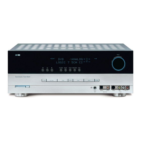
Page 6: Front Panel Controls
AVR147 FRONT-PANEL CONTROLS Main Power Switch: Surround Select: This mechanical switch turns the power supply After you have selected the desired surround on or off. It is usually left pressed in (On position), and cannot be turned mode group, press this button to select a specific mode. - Page 7 AVR147 Source Digital Input Message Display Speaker Size Indicators Select Tone Mode Setup Speaker/Channel Channel Level Navigation Surround Mode Indicators Delay Volume Input Indicators Adjust Headphone Jack/EzSet/EQ Digital Power Surround Tuning Preset Stations Microphone Video 3 Indicator Mode Input...
-
Page 8: Rear Panel Connections
This specialized connector may be used with video signals between devices. Although the AVR 147 is not capable of your personal computer in case Harman Kardon offers a software processing HDMI signals, if your video display is HDMI-capable, you may upgrade for the receiver at some time in the future. - Page 9 AVR147 HDMI 1 Input HDMI Output HDMI 2 Input Video 2 Video 1 Video Monitor Antenna Component Video Coaxial Digital RS-232 AC Power Inputs Outputs Jack Monitor Outputs Audio Inputs Serial Port Cord FM Antenna Inputs (1 & 2)
-
Page 10: Remote Control Functions
AVR147 REMOTE CONTROL FUNCTIONS The AVR 147 remote is capable of controlling up to ten devices, including Press the AVR Button so that you can access the Volume Controls. the AVR itself and an iPod docked in the optional The Bridge accessory. - Page 11 AVR147 IR Transmitter Lens Power On Mute Program Indicator Power Off AVR Selector Input Selectors 6-Channel Input Selector AM/FM XM Radio Test Tone TV/Video Sleep Volume Controls DSP Surround Not Used On-Screen Display Speaker Setup Channel Level Navigation Digital Input...
-
Page 12: Night Mode
AVR147 REMOTE CONTROL FUNCTIONS Volume Controls: Press these buttons to raise or lower the volume, ⁄ ¤ Buttons to select a letter (A through E) representing one of which will be shown in decibels (dB) in the Message Display. -
Page 13: Connections/Installation
AVR147 CONNECTIONS There are different types of audio and video connections used to Bare wire cables are installed as follows (see Figure 2): connect the receiver to the speakers and video display, and to connect 1. Unscrew the terminal cap until the pass-through hole in the collar the source devices to the receiver. -
Page 14: Audio Connections
Figure 7 – Multichannel Analog Audio Coaxial digital audio jacks are usually color-coded in orange. Although Harman Kardon receivers also include a proprietary, dedicated audio they look similar to analog jacks, they should not be confused, and you connection called “The Bridge/DMP”. If you own an iPod with a dock... - Page 15 The RS-232 serial port on the AVR 147 is used only for data. If components using separate wires contained within a single cable. The Harman Kardon releases a software upgrade for the receiver’s operating plug on an S-video cable contains four metal pins, plus a plastic guide system at some time in the future, the upgrade may be downloaded pin.
- Page 16 AVR147 INSTALLATION You are now ready to connect your various components to your receiver. Step Three – Connect the Antennas Before beginning, make sure that all components, including the AVR 147, Connect the FM and AM antennas to their terminals. See Figure 18.
- Page 17 AVR147 INSTALLATION We recommend connecting your various sources using the connections NOTE: It’s possible for a source to use none of the connections shown in Table 2 below in order to simplify programming your receiver named for that source. For example, you might connect your and remote control.
- Page 18 AVR147 INSTALLATION Figure 21 – Video 3 A/V and Digital Audio Inputs NOTE: If you receive your television programming using your TV with an antenna or direct cable connection, connect the TV’s analog and optical digital audio outputs (if available) to the Video 3 Analog Audio inputs and to the Coax or Optical 3 Figure 19 –...
- Page 19 Interface) input, you may use an HDMI-to-DVI adapter (not included). No video connections are needed. Bridge With Harman Kardon’s optional The Bridge, you can enjoy audio, video Figure 24 – HDMI 1 and Coaxial 2 Inputs or still images stored on your iPod (not included), use your AVR 147 remote control to operate the iPod, and even charge the iPod while it’s...
- Page 20 Video 1, the next time you press the DVD/CD Selector, the remote will return to the CD device mode. The AVR 147’s remote is factory-programmed to control an iPod docked in The Bridge and many Harman Kardon DVD and CD players.
- Page 21 Alternatively, you it until the Program LED starts to flash, then release it. Next, press may wish to consider purchasing Harman Kardon’s optional TC 30 the Input Selector that corresponds to the device type you want to activity-based remote, which is programmed by accessing a large program into the HDMI 2 mode, i.e., DVD, VCR/PVR or CBL/SAT.
- Page 22 AVR147 INSTALLATION Step Nine – Turn On the AVR 147 Two steps are required the first time you turn on the AVR 147. 1. Gently press the Master Power Switch until the word OFF is no longer visible. The Power Indicator above the two power switches should light up in amber, indicating that the AVR is in Standby mode and is ready to be turned on.
-
Page 23: Operation
AVR147 OPERATION Now that you have installed your system components and completed the Master Power Switch. When the Master Power Switch is turned off, at least a basic configuration of your receiver, you are ready to begin any settings you have programmed, including system configuration and enjoying your home theater system. -
Page 24: Mute Function
AVR147 OPERATION Mute Function NOTE: The AVR 147 does not have a conventional balance control. The EzSet/EQ process compensates for any characteristics To temporarily mute all speakers and the headphones, press the Mute of your room or speakers, and we recommend that you leave Button on the remote. -
Page 25: Audio Input Selection
AVR147 OPERATION button lighting up in red. Press that Input Selector again quickly to select display on the front panel are assigned to the Component Video 2 the source whose name appears above the button (i.e., CD, The Bridge... -
Page 26: Using The Tuner
AVR147 OPERATION then connect the player’s composite or S-video output to the AVR’s Using the Tuner corresponding DVD video input. The AVR 147’s built-in tuner may be selected in one of three ways c) Connect the player’s 6-channel analog audio outputs to the AVR’s... -
Page 27: Xm Radio Operation
AVR147 OPERATION To store a station in one of the 30 presets (see Figure 71): 2. Press the Tuning Buttons on the front panel or remote to scan through the channels. Auto tuning mode is not available. 1. Tune the desired station. - Page 28 AVR147 OPERATION NOTES: Table 5 – Using The Bridge 1. Analog audio signals are not converted to digital form, and iPod Function Remote Control Key Front-Panel Button digital audio signals are not converted to analog audio form. › Play...
-
Page 29: Selecting A Surround Mode
AVR147 OPERATION Selecting a Surround Mode Surround mode selection can be as simple or sophisticated as your individual system and tastes. Feel free to experiment with the many available surround modes on the AVR 147, and you may find a few that become your favorites for certain sources or program types. -
Page 30: Troubleshooting Guide
• Amplifier is in protection mode • Contact your local Harman Kardon service center due to internal problems No sound from surround or • Incorrect surround mode • Select a mode other than Stereo center speakers •... -
Page 31: Remote & Processor Resets
Tone Mode Button for at least 5 seconds until the RESET message appears in the display. If the receiver still does not function correctly after a processor reset, contact an authorized Harman Kardon service center for assistance. Service centers may be located by visiting our Web site at www.harmankardon.com. -
Page 32: Disassembly
AVR147 DISASSEMBLY AVR147 1. Removing the Top Cabinet 3. Removing the Rear Panel Remove the Screws Remove the Screws 24 25 4. Removing the Main PCB Remove the Screws 2. Removing the Front Panel Remove the Screws... - Page 33 AVR147 AVR147 DISASSEMBLY PROCEDURES 1 TOP-CABINET (21) REMOVAL 1. Remove 13 screws (S1,S7) and then remove the Top-cabinet. 2 FRONT PANEL ASS’Y REMOVAL 1. Remove the Top-cabinet, referring to the previous step 1. 2. Disconnect the card cable between connector (CN72-17p) on the Fip PCB (37-1)and connector (CN72) on the Input PCB (39-1).
- Page 34 AVR147 3. Disconnect the lead wire (BN84-5P) on the Fip PCB (37-1) from connector (CN84) on the Volume PCB (37-6). 4. Disconnect the lead wire (BN85-3P) on the Fip PCB (37-1) from connector (CN85) on the Phone PCB (37-5).
- Page 35 AVR147 5. Disconnect the board to board connector between and connector (CN23) on the XM PCB (42) and connector (BN17- 12P) on the iPod PCB (39-2). 6. Remove 1 screw (S15) and then remove the XM PCB (42). 12 HDMI PCB (47) REMOVAL 1.
- Page 36 AVR147 16 MAIN PCB ASS’Y(38-1) REMOVAL 1. Remove the Top-cabinet, referring to the previous step 1. 2. Remove the Tuner module (43), referring to the previous step 8. 3. Remove the Video PCB (41) referring to the previous step 9.
-
Page 37: Unit Exploded View
AVR147 AVR147 EXPLODED VIEW 37-7 40-1 40-3 39-2 40-4 39-1 40-5 40-2 38-1 38-2 40-2 DESCRIPTION PARTS NO. Q,ty Weright ORNAMENT,VOLUME CGU1A318Z CAP,VOLUME CGX1A338MBC63 HOLDER,VOLUME CMH1A214 INDICATOR,VOLUME CGL1A222 WINDOW ASS'Y CGUAVR145 WINDOW,FIP CGU1A399Y BADGE,MODEL CGB1A178Z SHEET,VOLUME CMZ2A090 FILTER,FIP CMZ1A088... -
Page 38: Exploded View Parts List
AVR147... -
Page 39: Amp Bias Adjustment
AVR147 AMPLIFIER SECTION BIAS ADJUSTMENT Measurement condition .No input signal or volume position is minimum. Standard value .Ideal current = 48mA (± 5%) .Ideal DC Voltage = 25.92mV (± 5%) DC EVM CUP11911* (MAIN PCB) CN61 CN64 CN63 CN65... - Page 40 AVR147...
-
Page 41: Pcb Drawings
AVR147... - Page 42 AVR147...
- Page 43 AVR147...
- Page 44 AVR147...
- Page 45 AVR147...
- Page 46 AVR147...
- Page 47 AVR147...
- Page 48 AVR147...
- Page 49 AVR147...
- Page 50 AVR147...
- Page 51 AVR147...
-
Page 52: Electrical Parts List
AVR147 AVR147 Electrical Parts List Ref. Designator Part Number Description FRONT PCB ASSY CUP11910-1 Capacitors C714 HCBS1H151KBT CAP , CERAMIC 150UF 50V K C716 CCEA1AH331T CAP , ELECT 330UF 10V C723 HCBS1H104ZFT CAP , CERAMIC 0.1UF 50V Z C728... - Page 53 AVR147 Ref. Designator Part Number Description FRONT PCB ASSY CUP11910-1 R920 CRD20TJ102T RES , CARBON 1K OHM 1/5W J Miscellaneous L702 HLQ02C100KT COIL , AXAIL 10uH BK71 CMD1A209 BRACKET , FLT BRACKET BK72 CMD1A209 BRACKET , FLT BRACKET BK73...
- Page 54 AVR147 Ref. Designator Part Number Description PCB , FRONT PANEL KEY CUP11910-2 R755 CRD20TF1801T RES , CARBON 1.8K /1/5W /F R756 CRD20TF2701T RES , CARBON 2.7K /1/5W/F R757 CRD20TF3301T RES , CARBON 3.3K /1/5W/F R758 CRD20TF5601T RES , CARBON 5.6K/1/5W/F...
- Page 55 AVR147 Ref. Designator Part Number Description PCB , VR JACK CUP11910-6 C874 HCBS1H101KBT CAP , CERAMIC 100PF 50V K Semiconductors IC87 HVINJM2068MDTE1 I.C , DUAL OP AMP D774 CVD1SS133MT DIODE 1SS133 D701 CVD52CSBBCEAB2 BLUE L.E.D L.E.D D703 CVD52CSBBCEAB2 BLUE L.E.D L.E.D...
- Page 56 AVR147 Ref. Designator Part Number Description PCB , PHONE JACK CUP11910-5 C852 HCBS1H104ZFT CAP , CERAMIC 0.1UF 50V Z C866 CCEA1HKS100T CAP , ELECT 10UF 50V C867 CCEA1HKS100T CAP , ELECT 10UF 50V C868 CCEA1EKS470T CAP , ELECT 47UF 25V...
- Page 57 AVR147 Ref. Designator Part Number Description PCB , PHONE JACK CUP11910-5 JW83 CWE8202150RV WIRE ASS'Y WIRE CN85 CJP03GA19ZY WAFER, STRAIGHT, 3PIN WAFER CN92 CJP05GA19ZY WAFER, STRAIGHT, 5PIN WAFER BN18 CWZAVR125BN18 WIRE ASS'Y (SHIELD) WIRE BN22 CWZAVR145BN22 WIRE ASS'Y (SHIELD)
- Page 58 AVR147 Ref. Designator Part Number Description MAIN PCB/HEATSINK (CUP11911) C917 HCQI1H473JZT CAP , MYLAR 0.047UF 50V J C924 CCFT1H104ZF CAP , SEMICONDUCTOR 0.1UF 50V ZF C939 CCEA1HH4R7T CAP , ELECT 4.7UF 50V C940 CCEA1AH471T CAP , ELECT 470UF 10V...
- Page 59 AVR147 Ref. Designator Part Number Description MAIN PCB/HEATSINK (CUP11911) D973 CVD1SS133MT DIODE 1SS133 D974 CVD1SS133MT DIODE 1SS133 D979 HVDMTZJ6.2BT DIODE , ZENER MTZJ6.2B D980 CVD1SS133MT DIODE 1SS133 Q501 HVTKTA1268GRT KTA1268GR TRANSISTOR PNP Q502 HVTKTA1268GRT TRANSISTOR PNP KTA1268GR Q503 HVTKTA1268GRT...
- Page 60 AVR147 Ref. Designator Part Number Description MAIN PCB/HEATSINK (CUP11911) Q882 HVT2SC3423O TRANSISTOR NPN POWER 2SC3423O Q883 HVT2SC3423O TRANSISTOR NPN POWER 2SC3423O Q884 HVT2SC3423O TRANSISTOR NPN POWER 2SC3423O Q885 HVT2SC3423O TRANSISTOR NPN POWER 2SC3423O IC94 HVIMC7805C I.C, REGULATOR(+5V) FAIRCHILD IC97 HVIS-80842CNY-X I.C RESET...
- Page 61 AVR147 Ref. Designator Part Number Description MAIN PCB/HEATSINK (CUP11911) R568 CRD20TJ561T RES , CARBON 560 OHM 1/5W J R569 CRD20TJ561T RES , CARBON 560 OHM 1/5W J R570 CRD20TJ561T RES , CARBON 560 OHM 1/5W J R571 CRD20TJ561T RES , CARBON...
- Page 62 AVR147 Ref. Designator Part Number Description MAIN PCB/HEATSINK (CUP11911) R654 CRD25FJ3R3T RES , CARBON 3.3 OHM 1/4W J R655 CRD25FJ3R3T RES , CARBON 3.3 OHM 1/4W J R666 CRD25TJ470T RES , CARBON 47 OHM 1/4W R667 CRD25TJ470T RES , CARBON...
- Page 63 AVR147 Ref. Designator Part Number Description MAIN PCB/HEATSINK (CUP11911) R944 CRD25TJ223T RES , CARBON 22K OHM 1/4W J R946 CRD25TJ223T RES , CARBON 22K OHM 1/4W J R947 CRD20TJ223T RES , CARBON 22K OHM 1/5W J R948 CRD25TJ222T RES , CARBON 2.2K OHM 1/4W J...
- Page 64 AVR147 Ref. Designator Part Number Description MAIN PCB/HEATSINK (CUP11911) JK92 CJJ5P020Z TERMINAL , SPEAKER TERMINAL JW90 CWE8212120VV WIRE , RED WIRE JW91 CWE8212180VV WIRE ASS'Y WIRE JW92 CWEE212080VV WIRE ASS'Y WIRE JW93 CWEP202110VV WIRE WIRE L501 CLEY0R5KAK COIL , SPEAKER 0.5UH...
- Page 65 AVR147 Ref. Designator Part Number Description PCB , POWER TRANS CUP11916-3,4 C921 HCQI1H104JZT CAP , MYLAR 0.1UF 50V J C922 HCQI1H104JZT CAP , MYLAR 0.1UF 50V J C923 HCQI1H104JZT CAP , MYLAR 0.1UF 50V J C924 HCQI1H104JZT CAP , MYLAR 0.1UF 50V J...
- Page 66 AVR147 Ref. Designator Part Number Description PCB , POWER TRANS CUP11916-3,4 R917 CRD20TJ153T RES , CARBON 15K OHM 1/5W J R918 CRD20TJ153T RES , CARBON 15K OHM 1/5W J R919 CRD20TJ153T RES , CARBON 15K OHM 1/5W J R920...
- Page 67 AVR147 Ref. Designator Part Number Description PCB , DIGITAL IN/OUT CUP11916-1 R766 CRD20TJ472T RES , CARBON 4.7K OHM 1/5W J R767 CRD20TJ472T RES , CARBON 4.7K OHM 1/5W J R768 CRD20TJ472T RES , CARBON 4.7K OHM 1/5W J R770...
- Page 68 AVR147 Ref. Designator Part Number Description PCB , REGULATOR CUP11916-5,6 C939 CCEA1EH101T CAP , ELECT 100UF 25V C940 CCEA1EH101T CAP , ELECT 100UF 25V C912 CCEA0JKR3222E CAP , ELECT 2200UF 6.3V C929 CCEA1VH102E CAP , ELECT 1000UF 35V C930...
- Page 69 AVR147 Ref. Designator Part Number Description PCB , INPUT CUP11912-1 C291 CCUS1H104KC CAP , CHIP 0.1UF C293 CCUS1H104KC CAP , CHIP 0.1UF C299 CCUS1H104KC CAP , CHIP 0.1UF C301 CCUS1H471JA CAP , CHIP 470PF C302 CCUS1H471JA CAP , CHIP...
- Page 70 AVR147 Ref. Designator Part Number Description PCB , INPUT CUP11912-1 C609 CCUS1H104KC CAP , CHIP 0.1UF C611 CCUS1H104KC CAP , CHIP 0.1UF C613 CCUS1H104KC CAP , CHIP 0.1UF C615 CCUS1H104KC CAP , CHIP 0.1UF C617 CCUS1H104KC CAP , CHIP 0.1UF...
- Page 71 AVR147 Ref. Designator Part Number Description PCB , INPUT CUP11912-1 C268 CCEA1EH470T CAP , ELECT 47UF 25V C272 CCEA1HH100T CAP , ELECT 10UF 50V C273 CCEA1HH100T CAP , ELECT 10UF 50V C275 CCEA1HH100T CAP , ELECT 10UF 50V C276...
- Page 72 AVR147 Ref. Designator Part Number Description PCB , INPUT CUP11912-1 C737 CCEA1CH101T CAP , ELECT 100UF 16V C740 CCEA1CH101T CAP , ELECT 100UF 16V C749 CCEA1CH101T CAP , ELECT 100UF 16V C764 CCEA0JH102T CAP , ELECT 1000UF 6.3V C766...
- Page 73 AVR147 Ref. Designator Part Number Description PCB , INPUT CUP11912-1 Resistors RN61 CRJ104DJ103T RES , 4ARRAY (1608*4) 10K OHM/1608*4 RN62 CRJ104DJ103T RES , 4ARRAY (1608*4) 10K OHM/1608*4 RN63 CRJ104DJ103T RES , 4ARRAY (1608*4) 10K OHM/1608*4 RN64 CRJ104DJ101T RES , 4ARRAY (1608*4)
- Page 74 AVR147 Ref. Designator Part Number Description PCB , INPUT CUP11912-1 R240 CRJ10DJ474T RES , CHIP 470K OHM R241 CRJ10DJ474T RES , CHIP 470K OHM R242 CRJ10DJ474T RES , CHIP 470K OHM R245 CRJ10DJ474T RES , CHIP 470K OHM R246...
- Page 75 AVR147 Ref. Designator Part Number Description PCB , INPUT CUP11912-1 R328 CRJ10DJ103T RES , CHIP 10K OHM R329 CRJ10DJ512T RES , CHIP 5.1K OHM R330 CRJ10DJ122T RES , CHIP 1.2K OHM R331 CRJ10DJ122T RES , CHIP 1.2K OHM R332...
- Page 76 AVR147 Ref. Designator Part Number Description PCB , INPUT CUP11912-1 R740 CRJ10DJ820T RES , CHIP 820 OHM R741 CRJ10DJ330T RES , CHIP 33 OHM R742 CRJ10DJ330T RES , CHIP 33 OHM R743 CRJ10DJ330T RES , CHIP 33 OHM R744...
- Page 77 AVR147 Ref. Designator Part Number Description PCB , INPUT CUP11912-1 CN72 CJP17GA117ZY WAFER WAFER ET02 CMD1A570 BRACKET , PCB BARCKET JK11 CJJ4R019W TERMINAL , IN/OUT TERMINAL JK12 CJJ4P014W JACK , IN/OUT JACK JK13 CJJ4R019W TERMINAL , IN/OUT TERMINAL JK14...
- Page 78 AVR147 Ref. Designator Part Number Description IPOD PCB(CUP11912-2) R438 CRJ10DJ222T RES , CHIP 2.2K OHM R439 CRJ10DJ222T RES , CHIP 2.2K OHM R440 CRJ10DJ220T RES , CHIP 2.2K OHM R441 CRJ10DJ472T RES , CHIP 4.7K OHM R442 CRJ10DJ472T RES , CHIP 4.7K OHM...
- Page 79 AVR147 Ref. Designator Part Number Description XM PCB (CUP11920) C507 CCUS1H104KC CAP , CHIP 0.1UF C508 CCUS1H104KC CAP , CHIP 0.1UF C509 CCUS1H104KC CAP , CHIP 0.1UF C510 CCUS1H104KC CAP , CHIP 0.1UF C511 CCUS1H104KC CAP , CHIP 0.1UF...
- Page 80 AVR147 Ref. Designator Part Number Description XM PCB (CUP11920) R528 CRJ10DJ223T RES , CHIP 22K OHM R529 CRJ10DJ223T RES , CHIP 22K OHM R530 CRJ10DJ223T RES , CHIP 22K OHM Miscellaneous X501 COX45158E180S X-TAL, 45.1584MHz (SMD) 45.1584MHz BK51 CMD1A569...
- Page 81 AVR147 Ref. Designator Part Number Description PCB , VIDEO CUP11917 C701 CCUS1H330JA CAP , CHIP 33PF C702 CCUS1H330JA CAP , CHIP 33PF C705 CCUS1H181JA CAP , CHIP 180PF C717 CCUS1H220JA CAP , CHIP 22PF C721 CCUS1H560JA CAP , CHIP...
- Page 82 AVR147 Ref. Designator Part Number Description PCB , VIDEO CUP11917 Semiconductors D502 HVDRLS4148SR DIODE, SWITCHING, SMD TYPE RLS4148 TE-11 D505 HVDRLS4148SR DIODE, SWITCHING, SMD TYPE RLS4148 TE-11 D512 HVDRLS4148SR DIODE, SWITCHING, SMD TYPE RLS4148 TE-11 D514 HVDRLS4148SR DIODE, SWITCHING, SMD TYPE...
- Page 83 AVR147 Ref. Designator Part Number Description PCB , VIDEO CUP11917 R493 CRJ10DJ750T RES , CHIP 75 OHM R501 CRJ10DJ333T RES , CHIP 33K OHM R502 CRJ10DJ680T RES , CHIP 68 OHM R503 CRJ10DJ123T RES , CHIP 12K OHM R504...
- Page 84 AVR147 Ref. Designator Part Number Description PCB , VIDEO CUP11917 R717 CRJ10DJ271T RES , CHIP 270 OHM R721 CRJ10DJ222T RES , CHIP 2.2 OHM R724 CRJ10DJ393T RES , CHIP 39J OHM R725 CRJ10DJ152T RES , CHIP 1.5K OHM R726...
- Page 85 AVR147 Ref. Designator Part Number Description CNVM9001MS0J72L AVR 147 TUNER MODULE...
-
Page 86: Semiconductor Pinouts
AVR147 AK4384 106dB 192kHz 24-Bit 2ch ∆Σ DAC GENERAL DESCRIPTION The AK4384 offers the perfect mix for cost and performance based audio systems. Using AKM's multi bit architecture for its modulator the AK4384 delivers a wide dynamic range while preserving linearity for improved THD+N performance. - Page 87 AVR147 ASAHI KASEI [AK4384] n Ordering Guide -40 ∼ +85°C AK4384VT 16pin TSSOP (0.65mm pitch) AKD4384 Evaluation Board for AK4384 n Pin Layout MCLK DZFL BICK DZFR SDTI LRCK View VCOM SMUTE/CSN AOUTL ACKS/CCLK AOUTR DIF0/CDTI PIN/FUNCTION Pin Name...
- Page 88 AVR147 IC51 XM IC...
- Page 89 AVR147...
- Page 90 AVR147...
- Page 91 AVR147...
- Page 92 AVR147...
- Page 93 AVR147...
- Page 94 AVR147 ST202E ST232E 15KV ESD PROTECTED 5V RS-232 TRANSCEIVER ESD PROTECTION FOR RS-232 I/O PINS: 15 KV HUMAN BODY MODEL GUARANTEED 120 kbps DATE RATE GUARANTEED SLEW RATE RANGE 3 to 30V/ µ s OPERATE FROM A SINGLE 5V POWER...
- Page 95 AVR147 ST202E/ST232E PIN CONFIGURATION PIN DESCRIPTION PIN No SYMBOL NAME AND F UNCTION Positive Terminal for the first Charge Pump Capacitor Doubled Voltage Terminal Negative Terminal for the first Charge Pump Capacitor Positive Terminal for the second Charge Pump Capacitor...
- Page 96 AVR147...
- Page 97 AVR147...
- Page 98 AVR147...
- Page 99 AVR147...
- Page 100 AVR147...
- Page 101 AVR147...
- Page 102 AVR147...
- Page 103 AVR147...
- Page 104 AVR147...
- Page 105 AVR147...
- Page 106 AVR147...
- Page 107 AVR147...
- Page 108 AVR147...
- Page 109 AVR147...
- Page 110 AVR147...
- Page 111 AVR147 Excel Semiconductor inc. ES29LV800E 8Mbit(1M x 8/512K x 16) CMOS 3.0 Volt-only, Boot Sector Flash Memory GENERAL FEATURES • Minimum 100,000 program/erase cycles per sector • 20 Year data retention at 125 • Single power supply operation - 2.7V -3.6V for read, program and erase operations SOFTWARE FEATURES •...
- Page 112 AVR147 Excel Semiconductor inc. GENERAL PRODUCT DESCRIPTION The ES29LV800 is completely compatible with the The ES29LV800 is a 8 megabit, 3.0 volt-only flash JEDEC standard command set of single power sup- memory device, organized as 1M x 8 bits (Byte ply Flash.
- Page 113 AVR147 Excel Semiconductor inc. PRODUCT SELECTOR GUIDE Family Part Number ES29LV800 Voltage Range 2.7 ~ 3.6V Speed Option Max Access Time (ns) CE# Access (ns) OE# Access (ns) FUNCTION BLOCK DIAGRAM RY/BY# Timer/ Vcc Detector DQ0-DQ15(A-1) Counter Analog Bias...
- Page 114 AVR147 Excel Semiconductor inc. PIN DESCRIPTION Description A0-A18 19 Addresses DQ0-DQ14 15 Data Inputs/Outputs DQ15 (Data Input/Output, Word Mode) DQ15/A-1 A-1 (LSB Address Input, Byte Mode) Chip Enable Output Enable Write Enable RESET# Hardware Reset Pin, Active Low BYTE#...
-
Page 115: Connection Diagram
AVR147 Excel Semiconductor inc. CONNECTION DIAGRAM BYTE# DQ15/A-1 48-Pin Standard TSOP DQ14 DQ13 DQ12 RESET# ES29LV800 DQ11 RY/BY# DQ10 48-Ball FBGA (6 x 8 mm) (Top View, Balls Facing Down) DQ15/ BYTE# DQ14 DQ13 DQ12 RESET# DQ10 DQ11... -
Page 116: Ordering Information
AVR147 HY57V161610E 2 Banks x 512K x 16 Bit Synchronous DRAM DESCRIPTION THE Hynix HY57V161610E is a 16,777,216-bits CMOS Synchronous DRAM, ideally suited for the main memory and graphic appli- cations which require large memory density and high bandwidth. HY57V161610E is organized as 2banks of 524,288x16. - Page 117 AVR147 HY57V161610E PIN CONFIGURATION DQ15 DQ15 DQ14 DQ14 VSSQ VSSQ DQ13 DQ13 DQ12 DQ12 VDDQ VDDQ DQ11 DQ11 DQ10 DQ10 VSSQ VSSQ VDDQ VDDQ 50pin TSOP II 50pin TSOP II VDDQ VDDQ 400mil x 825mil 400mil x 825mil LDQM LDQM 0.8mm pin pitch...
-
Page 118: Functional Block Diagram
AVR147 HY57V161610E FUNCTIONAL BLOCK DIAGRAM 1Mx16 Synchronous DRAM Self Refresh Counter Refresh Refresh Interval Timer Counter 512Kx16 Bank 0 Address[0:10] Sense AMP & I/O gates Column Decoder Address Precharge Register Row Active BA(A11) Column Addr. Column Active Latch & Counter... - Page 119 AVR147 HY57V161610E COMMAND TRUTH TABLE A10/ Command CKEn-1 CKEn A0~A9 Note Mode Register Set OP code No Operation Bank Active Row Address Read Column Address Read with Auto precharge Write Column Address Write with Auto precharge Precharge All Bank...
- Page 120 AVR147 Philips Semiconductors Product specification Hex inverter 74HCU04 FEATURES • Output capability: standard • I category: SSI GENERAL DESCRIPTION The 74HCU04 is a high-speed Si-gate CMOS device and is pin compatible with low power Schottky TTL (LSTTL). It is specified in compliance with JEDEC standard no. 7A.
- Page 121 AVR147 Philips Semiconductors Product specification Hex inverter 74HCU04 PIN DESCRIPTION PIN NO. SYMBOL NAME AND FUNCTION 1, 3, 5, 9, 11, 13 1A to 6A data inputs 2, 4, 6, 8, 10, 12 1Y to 6Y data outputs ground (0 V) positive supply voltage Fig.1 Pin configuration.
- Page 122 AVR147 74ACT04 HEX INVERTER HIGH SPEED: t = 5.0ns (TYP.) at V = 5V LOW POWER DISSIPATION: = 2µA(MAX.) at T =25°C COMPATIBLE WITH TTL OUTPUTS = 2V (MIN.), V = 0.8V (MAX.) 50Ω TRANSMISSION LINE DRIVING CAPABILITY TSSOP...
- Page 123 AVR147 NJM2595 5-INPUT 3-OUTPUT VIDEO SWITCH GENERAL DESCRIPTION PACKAGE OUTLINE The NJM2595 is a 5-input 3-output video switch. Its switches select one from five signals received from VTR,TV,DVD, TV-GAME and others. The NJM2595 is designed for audio items, such as AV amplifier and others.
- Page 124 AVR147 NJM2595 EQUIVALENT CIRCUIT PIN No. PIN NAME INSIDE EQUIVALENT CIRCUIT VOLTAGE Vin1 Vin2 Vin3 Vin4 Vin5 Vout1 Vout2 Vout3 2.1k Vout...
- Page 125 AVR147 NJM2595 EQUIVALENT CIRCUIT PIN No. PIN NAME INSIDE EQUIVALENT CIRCUIT VOLTAGE TEST CIRCUIT Vout2.2 Vout2.1 Vout3.2 Vout3.1 75 Ω 75 Ω 75 Ω 75 Ω 0.1µF Vin1 Vin2 75 Ω 75 Ω 100µF 10µF 10µF 1 10µF 10µF 10µF...
- Page 126 AVR147...
- Page 127 AVR147...
- Page 128 AVR147...
- Page 129 AVR147...
- Page 130 AVR147...
- Page 131 AVR147...
- Page 132 AVR147...
- Page 133 AVR147...
- Page 134 AVR147...
- Page 135 AVR147...
- Page 136 AVR147...
- Page 137 AVR147...
- Page 138 AVR147 HCF4053B TRIPLE 2-CHANNEL ANALOG MULTIPLEXER/DEMULTIPLEXER LOW "ON" RESISTANCE : 125Ω (Typ.) OVER 15V p.p SIGNAL-INPUT RANGE FOR = 15V HIGH "OFF" RESISTANCE : CHANNEL LEAKAGE ± 100pA (Typ.) at V = 18V BINARY ADDRESS DECODING ON CHIP HIGH DEGREE OF LINEARITY : < 0.5% DISTORTION TYP.
- Page 139 AVR147 HCF4053B INPUT EQUIVALENT CIRCUIT PIN DESCRIPTION PIN No SYMBOL NAME AND FUNCTION 11, 10, 9 A, B, C Binary Control Inputs Inhibit Inputs 12, 13, 2, 1, ax,ay,bx,by,cx,cy Input/ IN/OUT 5, 3 Output OUT/IN ax or ay OUT/IN...
- Page 140 AVR147...
- Page 141 AVR147...
- Page 142 AVR147...
- Page 143 AVR147...
- Page 144 AVR147...
- Page 145 AVR147...
- Page 146 AVR147...
- Page 147 AVR147...
- Page 148 AVR147...
- Page 149 AVR147...
- Page 150 AVR147...
- Page 151 AVR147...
- Page 152 AVR147...
- Page 153 AVR147 AK4589 2/8-Channel Audio CODEC with DIR PVSS PVDD X'tal Clock Oscillato r 8 to 3 Recovery Clock MCKO1 Generator Input MCKO2 Selector LRCK2 DAIF A udio BICK2 Decode r SDTO2 DAUX2 A VDD A VSS DVDD Error &...
- Page 154 AVR147 ASAHI KASEI [AK4589] オーダリングガイド -10 ∼ +70°C AK4589VQ 80pin LQFP(0.5mm pitch) 評価ボード AKD4589 ピン配置 TEST1 INT1 BOUT TVDD DVDD AVSS DVSS AVDD VREFH XT I VCOM (Top View) TEST3 MCKO2 MCKO1 ROUT1+ COUT ROUT1- UOUT LOUT1+ VOUT LOUT1-...
- Page 155 AVR147 ASAHI KASEI [AK4589] AK4588 との相違点 Functions AK4588 AK4589 DAC 出力 シングルエンド 差動 DAC S/(N+D) 90dB 94dB DAC S/N 106dB 114dB Typ ±2.7Vpp DAC Output voltage Typ 3.0Vpp DAC AOUT AOUT=0.6xVREFH AOUT=0.54xVREFH Load Resistance 5k ohm 2k ohm ±1.0 Frequency Response 80kHz +0/-0.6...
- Page 156 AVR147 ASAHI KASEI [AK4589] ピン/機能 Pin Name Function INT1 Interrupt 1 Pin Block-Start Output Pin for Receiver Input BOUT “H” during first 40 flames. TVDD Output Buffer Power Supply Pin, 2.7V∼5.25V DVDD Digital Power Supply Pin, 4.75V∼5.25V DVSS Digital Ground Pin...
- Page 157 AVR147 ASAHI KASEI [AK4589] Pin Name Function Power-Down Mode Pin When “L”, the AK4589 is powered-down, all digital output pins go “L”, all registers are reset. When CAD1/0 pins are changed, the AK4589 should be reset by PDN pin.
- Page 158 AVR147 ASAHI KASEI [AK4589] Pin Name Function AVDD Analog Power Supply Pin, 4.75V∼5.25V Analog Ground Pin, 0V AVSS Receiver Channel 0 Pin (Internal biased pin. Internally biased at PVDD/2) No Connect pin No internal bonding. This pin should be connected to PVSS.
- Page 159 AVR147 ASAHI KASEI [AK4589] 使用しないピンの処理について 使用しない入出力ピンは下記の設定を行い、適切に処理して下さい。 Classification Pin Name Setting Analog RX0-7, LOUT1-4, ROUT1-4, LIN, RIN These pins should be open. INT0-1, BOUT, XTO, MCKO1-2, COUT, UOUT, These pins should be open. VOUT, SDTO1-2, CDTO, DZF1-2, TX1-0 Digital These pins should be connected to DVSS.
- Page 160 AVR147 Video Switch · 75Ω driver · Y/C mix MM1501 MITSUMI Video Switch · 75Ω driver · Y/C mix Monolithic IC MM1501 Series Outline This IC extends the series of ICs for video/audio signal switching, with a 2-input 1-output single video switch, video signal/chroma signal 75Ω...
-
Page 161: Block Diagram
AVR147 Video Switch · 75Ω driver · Y/C mix MM1501 MITSUMI Block Diagram MM1501 MM1502 MM1503 MM1504 MM1505 MM1506... - Page 162 AVR147 Video Switch · 75Ω driver · Y/C mix MM1501 MITSUMI MM1507 MM1508 MM1509 MM1510 MM1511 MM1512...
- Page 163 AVR147...
- Page 164 AVR147...
- Page 165 AVR147...
- Page 166 AVR147 M24C64 M24C32 64Kbit and 32Kbit Serial I²C Bus EEPROM FEATURES SUMMARY Two-Wire I C Serial Interface Figure 1. Packages Supports 400kHz Protocol Single Supply Voltage: – 4.5 to 5.5V for M24Cxx – 2.5 to 5.5V for M24Cxx-W –...
- Page 167 AVR147 M24C64, M24C32 SUMMARY DESCRIPTION These I C-compatible electrically erasable pro- Table 2. Signal Names grammable memory (EEPROM) devices are orga- E0, E1, E2 Chip Enable nized as 8192 x 8 bits (M24C64) and 4096 x 8 bits (M24C32).
- Page 168 AVR147 M24C64, M24C32 SIGNAL DESCRIPTION Serial Clock (SCL). This input signal is used to rial Data (SDA) to V (Figure 4. indicates how strobe all data in and out of the device. In applica- the value of the pull-up resistor can be calculated).
- Page 169 AVR147 M24C64, M24C32 MEMORY ORGANIZATION The memory is organized as shown in Figure Figure 6. Block Diagram High Voltage Control Logic Generator I/O Shift Register Address Register Data and Counter Register 1 Page X Decoder AI06899 7/26...
-
Page 170: Device Operation
AVR147 M24C64, M24C32 DEVICE OPERATION The device supports the I C protocol. This is sum- Data (SDA) Low to acknowledge the receipt of the marized in Figure 5.. Any device that sends data eight data bits. on to the bus is defined to be a transmitter, and Data Input any device that reads the data to be a receiver. - Page 171 AVR147 M24C64, M24C32 Figure 7. Write Mode Sequences with WC=1 (data write inhibited) NO ACK BYTE WRITE DEV SEL BYTE ADDR BYTE ADDR DATA IN NO ACK PAGE WRITE DEV SEL BYTE ADDR BYTE ADDR DATA IN 1 DATA IN 2...
- Page 172 AVR147 M24C64, M24C32 Page Write The bus master sends from 1 to 32 bytes of data, each of which is acknowledged by the device if The Page Write mode allows up to 32 bytes to be Write Control (WC) is Low. If Write Control (WC) is...
- Page 173 AVR147 M24C64, M24C32 Figure 9. Write Cycle Polling Flowchart using ACK WRITE Cycle in Progress START Condition DEVICE SELECT with RW = 0 Returned First byte of instruction with RW = 0 already decoded by the device Next Operation is...
- Page 174 AVR147 M24C64, M24C32 Figure 10. Read Mode Sequences NO ACK CURRENT ADDRESS DEV SEL DATA OUT READ NO ACK RANDOM ADDRESS DEV SEL * BYTE ADDR BYTE ADDR DEV SEL * DATA OUT READ NO ACK SEQUENTIAL CURRENT DEV SEL...
- Page 175 AVR147 LOW VOLTAGE DETECTOR × 5VT SERIES × PIN CONFIGURATION TO-92 • SOT-89 SOT-23-5 • • (mark side) (mark side) (mark side) PIN DESCRIPTION TO-92 SOT-89 SOT-23-5 • • • Pin No. Symbol Pin No. Symbol Pin No. Symbol...
- Page 176 AVR147 VOL TAGE DETECTOR × 5VL SERIES × PIN CONFIGURATION TO-92 SOT-89 SOT-23-5 • • • (mark side) (mark side) (mark side) PIN DESCRIPTION TO-92 SOT-89 SOT-23-5 • • • Pin No Symbol Pin No Symbol Pin No Symbol...
- Page 177 AVR147 1A LOWDROP OUT VOLTAGE REGULATOR (ADJUSTABLE & FIXED) LM1117 FEATURES SOT-223 PKG (FRONT VIEW) ● Output Current up to 1 A ● Low Dropout Voltage ( 700mV at 1A Output Current ) PIN FUNCTION ● Three Terminal Adjustable or Fixed 1.5V, 1.8V, 2.5V, 2.85V, 1.
- Page 178 AVR147 TRANSISTOR, REGULATOR IC BLOCK DIAGRAM TO-92L TO-92M TO-92 TO-220 1. Emitter 1. Emitter 1. Emitter 1. GND 2. Collector 2. Collector 2. Collector 2. INPUT 3. Base 3. Base 3. Base 3. OUTPUT 12 3 1 2 3...
- Page 179 AVR147 ULTRA-SMALL PACKAGE HIGH-PRECISION VOLTAGE DETECTOR Rev.3.2 S-808xxC Series Pin Configurations Table 7 SC-82AB Top view Pin No. Pin name Pin description Voltage detection output pin Voltage input pin No connection GND pin *1. The NC pin is electrically open.
-
Page 180: Absolute Maximum Ratings
AVR147 ULTRA-SMALL PACKAGE HIGH-PRECISION VOLTAGE DETECTOR Rev.3.2 S-808xxC Series S-80842CNY Table 11 TO-92 Bottom view Pin No. Pin name Pin description Voltage detection output pin Voltage input pin GND pin Figure 8 Absolute Maximum Ratings 1. Detection Voltage Typ. 1.4 V or Less Products Table 12 (Ta = 25 °... -
Page 181: Schematics
AVR147... - Page 182 AVR147...
- Page 183 AVR147...
- Page 184 AVR147...
- Page 185 AVR147...
- Page 186 AVR147...
- Page 187 AVR147...
- Page 188 AVR147...
- Page 189 AVR147...
-
Page 190: Wiring Diagram
AVR147...