Table of Contents
Advertisement
Quick Links
Advertisement
Table of Contents

Related Manuals for Clevo NL51CU


Summary of Contents for Clevo NL51CU
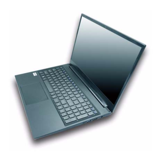
- Page 1 NL50CU / NL51CU...
- Page 3 Preface Notebook Computer NL50CU / NL51CU Service Manual...
- Page 4 Preface Notice The company reserves the right to revise this publication or to change its contents without notice. Information contained herein is for reference only and does not constitute a commitment on the part of the manufacturer or any subsequent ven- dor.
- Page 5 It is organized to allow you to look up basic information for servicing and/or upgrading components of the NL50CU / NL51CU series notebook PC. The following information is included: Chapter 1, Introduction, provides general information about the location of system elements and their specifications.
- Page 6 Preface IMPORTANT SAFETY INSTRUCTIONS Follow basic safety precautions, including those listed below, to reduce the risk of fire, electric shock and injury to per- sons when using any electrical equipment: 1. Do not use this product near water, for example near a bath tub, wash bowl, kitchen sink or laundry tub, in a wet basement or near a swimming pool.
- Page 7 Preface Instructions for Care and Operation The notebook computer is quite rugged, but it can be damaged. To prevent this, follow these suggestions: Don’t drop it, or expose it to shock. If the computer falls, the case and the components could be damaged. Do not expose the computer Do not place it on an unstable Do not place anything heavy...
- Page 8 Preface Avoid interference. Keep the computer away from high capacity transformers, electric motors, and other strong mag- netic fields. These can hinder proper performance and damage your data. Take care when using peripheral devices. Use only approved brands of Unplug the power cord before peripherals.
- Page 9 Preface Battery Precautions • Only use batteries designed for this computer. The wrong battery type may explode, leak or damage the computer. • Do not continue to use a battery that has been dropped, or that appears damaged (e.g. bent or twisted) in any way. Even if the computer continues to work with a damaged battery in place, it may cause circuit damage, which may possibly result in fire.
- Page 10 Preface Related Documents You may also need to consult the following manual for additional information: User’s Manual on CD/DVD This describes the notebook PC’s features and the procedures for operating the computer and its ROM-based setup pro- gram. It also describes the installation and operation of the utility programs provided with the notebook PC. System Startup 1.
-
Page 11: Table Of Contents
Preface Contents Introduction ..........1-1 Bottom ................... A-4 LCD ....................A-5 Overview ..................1-1 HDD ....................A-6 Specifications ..................1-2 MB ....................A-7 External Locator - Top View with LCD Panel Open ......1-4 Schematic Diagrams......... B-1 External Locator - Front & Right Side Views .........1-5 External Locator - Left Side &... - Page 12 Preface M Key PCIE SSD ................. B-27 3G/LTE ..................B-28 USB Type-A ................. B-29 Conn, CCD, Fan, TP ..............B-30 3V, 5V, 3VS, 5VS, 1.8V, 1.5VS ..........B-31 VDD3, VDD5 ................B-32 1.05VA, VCCST, VCCSTG ............B-33 VDDQ, VDDQ_VTT, 1.8VA ............B-34 Power PD Function ..............
-
Page 13: Introduction
Chapter 1: Introduction Overview This manual covers the information you need to service or upgrade the NL50CU / NL51CU series notebook computer. Information about operating the computer (e.g. getting started, and the Setup utility) is in the User’s Manual. Information about dri-vers (e.g. -
Page 14: Specifications
Introduction Specifications Processor Options Pointing Device Intel® Core™ i7 Processor Built-in Click pad (with Microsoft PTP Multi Gesture & Scroll- ing Functionality) i7-10510U (1.80GHz) 8MB Smart Cache, 14nm, DDR4-2666MHz, TDP 15W Keyboard Intel® Core™ i5 Processor Latest Specification Information i5-10210U (1.60GHz) Full-size Keyboard (with Numeric Keypad) 6MB Smart Cache, 14nm, DDR4-2666MHz, TDP 15W... - Page 15 Introduction Communication Power Built-In 10/100/1000Mb Base-TX Ethernet LAN Full Range AC/DC Adapter 1.0M HD Camera Module AC Input: 100 - 239.3V, 50 - 60Hz (Factory Option) 4G M.2 Module DC Output: 19V, 2.1A (40W) WLAN/ Bluetooth M.2 Modules: Embedded Lithium-Ion Polymer Battery Pack, 36WH (Factory Option) Intel®...
-
Page 16: External Locator - Top View With Lcd Panel Open
Introduction External Locator - Top View with LCD Panel Open Figure 1 Top View 1. PC Camera 2. *PC Camera LED *When the PC camera is in use, the LED will be illuminated in white. 3. Built-In Array Microphone 4. LCD 5. -
Page 17: External Locator - Front & Right Side Views
Introduction External Locator - Front & Right Side Views Figure 2 Front View FRONT VIEW Figure 3 Right Side View 1. Speaker 2. USB 3.1 Gen 2 Type-C Port 3. USB 3.1 Gen 2 RIGHT SIDE VIEW Type-A Port 4. HDMI-Out Port 5. -
Page 18: External Locator - Left Side & Rear View
Introduction External Locator - Left Side & Rear View Figure 4 Left Side View 1. Security Lock Slot 2. RJ-45 LAN Jack 3. MicroSD Card LEFT SIDE VIEW Reader 4. USB 2.0 Port 5. USIM Card Reader 6. 2-In-1 Audio Jack (Headphone and Microphone) 7. -
Page 19: External Locator - Bottom View
Introduction External Locator - Bottom View Figure 6 Bottom View 1. Vent 2. RJ-45 LAN Jack 3. Speakers Overheating To prevent your com- puter from overhea- ting, make sure no- thing blocks any vent while the computer is in use. External Locator - Bottom View 1 - 7... -
Page 20: Mainboard Overview - Top (Key Parts)
Introduction Mainboard Overview - Top (Key Parts) Figure 7 Mainboard Top Key Parts 1. KBC-ITE IT5570 1 - 8 Mainboard Overview - Top (Key Parts) -
Page 21: Mainboard Overview - Bottom (Key Parts)
Introduction Mainboard Overview - Bottom (Key Parts) Figure 8 Mainboard Bottom Key Parts 1. CPU 2. Memory Slots DDR4 SO-DIMM Mainboard Overview - Bottom (Key Parts) 1 - 9... -
Page 22: Mainboard Overview - Top (Connectors)
Introduction Mainboard Overview - Top (Connectors) Figure 9 Mainboard Top Connectors 1. DC-In Jack 2. HDMI-Out Port 3. USB 3.1 Gen 2 Type-A Port 4. USB 3.1 Gen 2 Type-C Port 5. LED Keyboard Connector 6. Keyboard Cable Connector 7. Power Switch Connector 1 - 10 Mainboard Overview - Top (Connectors) -
Page 23: Mainboard Overview - Bottom (Connectors)
Introduction Mainboard Overview - Bottom (Connectors) Figure 10 Mainboard Bottom Connectors 1. CCD Cable Connector 2. Fan Connector 3. M.2 Card Connector 4. Speaker Connecto 5. HDD Connector 6. Battery Connector 7. Touchpad Connector 8. USIM Card Reader Connector 9. USB Board Connector 10. - Page 24 Introduction 1 - 12...
-
Page 25: Disassembly
Chapter 2: Disassembly Overview This chapter provides step-by-step instructions for disassembling the NL50CU / NL51CU series notebook’s parts and subsystems. When it comes to reassembly, reverse the procedures (unless otherwise indicated). We suggest you completely review any procedure before you take the computer apart. -
Page 26: Maintenance Tools
Disassembly NOTE: All disassembly procedures assume that the system is turned OFF, and disconnected from any power supply (the battery is removed too). Maintenance Tools The following tools are recommended when working on the notebook PC: • M3 Philips-head screwdriver •... -
Page 27: Maintenance Precautions
Disassembly Maintenance Precautions The following precautions are a reminder. To avoid personal injury or damage to the computer while performing a removal and/or replacement job, take the following precautions: Power Safety Don't drop it. Perform your repairs and/or upgrades on a stable surface. If the computer falls, the case and other components Warning could be damaged. -
Page 28: Disassembly Steps
Disassembly Disassembly Steps The following table lists the disassembly steps, and on which page to find the related information. PLEASE PERFORM THE DISASSEMBLY STEPS IN THE ORDER INDICATED. To remove the Battery: To remove the CCD Module: 1. Remove the battery page 2 - 5 1. -
Page 29: Removing The Battery
Disassembly Removing the Battery Figure 1 Battery Removal 1. Turn off the computer, turn it over. 2. Remove screws on the bottom case (Figure 1a). a. Remove the screws. 3. Note to remove screws , do so with the screwdriver angled at about 90 degrees to the computer surface b. - Page 30 Disassembly 6. Carefully disconnect the cable , then remove screws (Figure 2d Figure 2 7. Lift the battery off the computer (Figure 2e Battery Removal 8. Reverse the process to install a new battery (do not forget to replace all the screws and bottom cover). (cont’d.) 9.
-
Page 31: Removing The Hard Disk Drive
Disassembly Removing the Hard Disk Drive Figure 3 The hard disk drive can be taken out to accommodate other 2.5" serial (SATA) hard disk drives with a height of 7.0mm HDD Assembly (h). Follow your operating system’s installation instructions, and install all necessary drivers and utilities (as outlined in Removal Chapter 4 of the User’s Manual) when setting up a new hard disk. - Page 32 Disassembly 5. Remove screws and bracket from the hard disk (Figure 4d Figure 4 6. Reverse the process to install a new hard disk (do not forget to replace the screws). HDD Assembly Removal (cont’d.) d. Remove the screws and bracket from the HDD.
-
Page 33: Removing The System Memory (Ram)
Disassembly Removing the System Memory (RAM) Figure 5 RAM Module The computer has two memory sockets for 260 pin Small Outline Dual In-line Memory Modules (SO-DIMM) supporting Removal DDR4 2400MHz. The main memory can be expanded up to 32GB. The total memory size is automatically detected by the POST routine once you turn on your computer. - Page 34 Disassembly 5. Pull the latches to release the second module if necessary. 6. Insert a new module holding it at about a 30° angle and fit the connectors firmly into the memory slot. 7. The module will only fit one way as defined by its pin alignment. Make sure the module is seated as far into the slot as it will go.
-
Page 35: Removing The Keyboard
Disassembly Removing the Keyboard Figure 6 1. Turn off the computer, turn it over to remove the battery (page 2 - Keyboard Removal 2. Locate the release points from the open bottom case (Figure 6a). 3. Open it up with the LCD on a flat surface before pressing at point to release the keyboard module (use the spe- cific eject stick to do this) while releasing the keyboard in the direction of the arrow... -
Page 36: Removing The Wireless Lan Module
Disassembly Removing the Wireless LAN Module Figure 7 Wireless LAN 1. Turn off the computer, turn it over to remove the battery (page 2 - Module Removal 2. The Wireless LAN module will be visible at point on the mainboard (Figure 7a). -
Page 37: Wireless Lan, And Combo Module Cables
Disassembly Wireless LAN, and Combo Module Cables Note that the cables for connecting to the antennae on WLAN, WLAN & Bluetooth Combo modules are not labelled. The cables/covers (each cable will have either a black or transparent cable cover) are color coded for identification as outlined in the table below. -
Page 38: Removing The 4G Module
Disassembly Removing the 4G Module Figure 8 4G Module Removal 1. Turn off the computer, turn it over to remove the battery (page 2 - 2. The module will be visible at point on the mainboard (Figure 7a). a. Locate the WLAN. 3. -
Page 39: Removing The M.2 Ssd Module
Disassembly Removing the M.2 SSD Module Figure 9 M.2 SSD Module 1. Turn off the computer, turn it over to remove the battery (page 2 - Removal 2. The M.2 SSD module will be visible at point on the mainboard (Figure 9a). -
Page 40: Removing The Ccd
Disassembly Removing the CCD Figure 10 CCD Removal 1. Turn off the computer, turn it over to remove the battery (page 2 - 2. Run your fingers around the inner frame of the LCD panel at the points as indicated by the arrows (Figure a. - Page 41 Disassembly 4. Disconnect the cable (Figure 11f). Figure 11 5. Remove the CCD module (Figure 11g). CCD Removal 6. Reverse the process to install a new CCD module. (cont’d.) c. Disconnect the cable. d. Remove the CCD mod- ule. 6.
- Page 42 Disassembly 2 - 18...
-
Page 43: Part Lists
Appendix A:Part Lists This appendix breaks down the NL50CU / NL51CU series notebook’s construction into a series of illustrations. The component part numbers are indicated in the tables opposite the drawings. Note: This section indicates the manufacturer’s part numbers. Your organization may use a different system, so be sure to cross-check any relevant documentation. -
Page 44: Part List Illustration Location
Part List Illustration Location The following table indicates where to find the appropriate part list illustration. Table A - 1 Part List Illustration Part Location page A - 3 page A - 4 Bottom page A - 5 page A - 6 page A - 7 A - 2... -
Page 45: Top
Figure A - 1 Top A - 3... -
Page 46: Bottom
Bottom Figure A - 2 Bottom A - 4 Bottom... -
Page 47: Lcd
Figure A - 3 LCD A - 5... -
Page 48: Hdd
Figure A - 4 A - 6 HDD... - Page 49 Figure A - 5 MB A - 7...
- Page 50 A - 8...
-
Page 51: Schematic Diagrams
Schematic Diagrams Appendix B: Schematic Diagrams This appendix has circuit diagrams of the NL50CU / NL51CU notebook’s PCB’s. The following table indicates where to find the appropriate schematic diagram. Diagram - Page Diagram - Page Diagram - Page Table B - 1... - Page 52 Schematic Diagrams System Block Diagram 5 IN 1 6-7P-NL4C5-002 NL40CU Comet LAKE U62 (HDCP2.2) System Block Diagram MAIN BOARD SHEET 2~38 6-71-NL4C0-D02 LAN BOARD 5V,5VS,3.3VA,3.3V 1866/ 2133 MHz 6-71-NL4CZ-D02 3.3VS,1.8V,1.5VS SHEET 39 DDI2 DDR4 SHEET 30 DDR4 14" I/O BOARD SO-DIMM A SHEET 16 HDMI...
- Page 53 Schematic Diagrams Processor 1/12 Comet Lake U A,D/20 DDI,MISC,JAG TYPE C+DP PORT eDP PANEL MDP_D#0 DDI1_TXN_0 EDP_TXN_0 EDP_TXN_0 MDP_D0 DDI1_TXP_0 EDP_TXP_0 EDP_TXP_0 MDP_D#1 EDP_TXN_1 DDI1_TXN_1 EDP_TXN_1 MDP_D1 DDI1_TXP_1 EDP_TXP_1 EDP_TXP_1 DIFF=85ohm MDP_D#2 DDI1_TXN_2 EDP_TXN_2 EDP_TXN_2 Length <6000 mils MDP_D2 EDP_TXP_2 DDI1_TXP_2 EDP_TXP_2 MDP_D#3...
- Page 54 Schematic Diagrams Processor 2/12 Comet Lake U B,C/20 DDR4 Interleave M_A_DQ[63:0] M_B_DQ[63:0] LP3 / DDR4 DDR4 (IL) / LP3 - DDR4 (NIL) M_A_CLK_DDR#0 LP3 / DDR4 AF28 M_A_DQ0 DDR0_CKN_0/DDR0_CKN_0 DDR4 (IL) / LP3 - DDR4 (NIL) DDR1_CKN_0/DDR1_CKN_0 M_B_CLK_DDR#0 M_B_DQ0 DDR0_DQ_0/DDR0_DQ_0 DDR0_CKP_0/DDR0_CKP_0 M_A_CLK_DDR0 AF29...
-
Page 55: Processor 11/12
Schematic Diagrams Processor 3/12 CFG0 CFG_0 RSVD_TP_1 RSVD_TP_2 CFG_1 CP36 IST_TRIG Comet Lake U Q/20 CFG CFG_2 CN36 CFG3 RSVD_TP_3 CFG_3 1K_04 R358 CFG4 CFG_4 *1K_04 R361 CFG5 BJ36 CFG_5 RSVD_5 *1K_04 R357 CFG6 BJ34 CFG_6 RSVD_6 CFG7 CFG_7 CFG[0]: Stall reset sequence after PCU PLL BK34 CFG_8 TP_3... - Page 56 Schematic Diagrams Processor 4/12 Comet Lake U E/20 SPI/SMB/LPC SPI_SCLK_R SMB_CLK CH37 CK14 R194 *0402_short SPI0_CLK GPP_C0/SMBCLK SMB_CLK_DDR 14,15 SPI_SO_R SMB_DATA R195 CF37 CH15 *0402_short SPI0_MISO GPP_C1/SMBDATA SMB_DAT_DDR 14,15 SPI_SI_R CF36 CJ15 PCH_GPP_C2 SPI_W P#_0 PCH_SPI_DQ2 SPI0_MOSI GPP_C2/SMBALERT# R504 49.9_1%_04 CF34 SPI_HOLD#_0 PCH_SPI_DQ3...
-
Page 57: Processor 12/12
Schematic Diagrams Processor 5/12 Comet Lake U F,G/20 GPIO/HDA R191 *10K_04 3.3VA CC27 GPP_B15/GSPI0_CS0# CC32 CN22 R417 0_04 SW I# TPM_PIRQ# PCH_GPP_B16 GPP_A7/PIRQA#/GSPI0_CS1# GPP_D9/ISH_SPI_CS#/GSPI2_CS0# CE28 CR22 GPP_B16/GSPI0_CLK GPP_D10/ISH_SPI_CLK/GSPI2_CLK PCH_GPP_B17 R161 100K_04 CE27 CM22 GPP_B17/GSPI0_MISO GPP_D11/ISH_SPI_MISO/GSPI2_MISO PCH_GPP_B18 CE29 CP22 PCH_GPP_D12 GPP_B18/GSPI0_MOSI GPP_D12/ISH_SPI_MOSI/GSPI2_MOSI CA31 CK22... - Page 58 Schematic Diagrams Processor 6/12 Comet Lake U H/20 PCIE,SATA,USB USB3_1RXN PCIE5_RXN/USB31_5_RXN PCIE1_RXN/USB31_1_RXN USB port1 (2.0+3.1) USB3_1RXP PCIE5_RXP/USB31_5_RXP PCIE1_RXP/USB31_1_RXP USB3.1 GEN2 Type-A PCIE5_TXN/USB31_5_TXN PCIE1_TXN/USB31_1_TXN USB3_1TXN USB3_1TXP PCIE5_TXP/USB31_5_TXP PCIE1_TXP/USB31_1_TXP USB3_2RXN PCIE6_RXN/USB31_6_RXN PCIE2_RXN/USB31_2_RXN/SSIC_1_RXN M/B USB port2 (2.0+3.1) PCIE6_RXP/USB31_6_RXP PCIE2_RXP/USB31_2_RXP/SSIC_1_RXP USB3_2RXP Type C PCIE6_TXN/USB31_6_TXN PCIE2_TXN/USB31_2_TXN/SSIC_1_TXN USB3_2TXN PCIE6_TXP/USB31_6_TXP...
- Page 59 Schematic Diagrams Processor 7/12 Comet Lake U I,J/20 CNVI/CLK 3.3VS CNVi CR30 CNVI_W R_D0N CNV_WR_D0N CPU_C10_GATE# CPU_C10_GATE# CP30 CN27 R418 *100K_04 D02 unstuff CPU_C10_GATE# 24,32,37 CNVI_W R_D0P CNV_WR_D0P GPP_H18/CPU_C10_GATE# CM30 CM27 CNVI_W R_D1N CNV_WR_D1N GPP_H19/TIMESYNC_0 CN30 3.3VA CNVI_W R_D1P CNV_WR_D1P GPPC_H21 CF25 GPP_H21/XTAL_FREQ_SELECT...
- Page 60 Schematic Diagrams Processor 8/12 VCCST Comet Lake U K/20 POWER CONTROL R253 3.3V 1K_04 H_VCCST_PW RGD R252 1M_04 Q16A MTDK3S6R D02 modify SLP_S0# 24,35 Q16B RSMRST# PLT_RST# SLP_S0# MTDK3S6R BJ35 BJ37 R392 *100K_04 GPP_B13/PLTRST# GPP_B12/SLP_S0# SYS_RESET# SUSB#_PCH D02 modify CN10 BU36 SYS_RESET# GPD4/SLP_S3#...
- Page 61 Schematic Diagrams Processor 9/12 Comet Lake U L,M/20 VCC,VCCGT VCC_CORE VCORE SVID VCC_CORE PLACE IN CPU BACK SIDE AW24 VCCCORE_28 VCCCORE_67 VCCGT AN10 AW25 VCCCORE_29 VCCCORE_68 AN24 AW26 C370 VCCGT SVID 31A C104 C126 C115 C114 VCCCORE_30 VCCCORE_69 AN26 AW27 VCCGT VCCCORE_31 VCCCORE_70...
- Page 62 Schematic Diagrams Processor 10/12 Comet Lake U N,O/20 VDDQ,VCCIO VDDQ FIX 3.3A 1.2V+5% VCCIO FIX 0.95V 4A VCCIO VDDQ PLACE IN CPU BACK SIDE PLACE IN CPU BACK SIDE 2.8A AK24 VCCIO_OUT_1 AD36 AK26 VDDQ_1 VCCIO_OUT_2 AH32 AL24 C154 C134 C135 VDDQ_2 VCCIO_OUT_3...
- Page 63 Schematic Diagrams Processor 11/12 Comet Lake U P/20 POWER 1.625A BP20 1.05VA VCCPRIM_1P05_5 BW16 CB16 199mA 3.3VA VCCPRIM_1P05_6 VCCPRIM_3P3_3 C164 1u_6.3V_X6S_04 BW18 VCCPRIM_1P05_7 VCC_RTC BW19 VCCPRIM_1P05_8 BY16 VCCPRIM_1P05_9 CA14 BR23 C149 1u_6.3V_X6S_04 VCCPRIM_1P05_10 VCCRTC C150 0.1u_6.3V_X5R_02 696mA CC15 BY20 1.625A 1.8VA 1.05VA VCCPRIM_1P8_6...
- Page 64 Schematic Diagrams Processor 12/12 Comet Lake U R,S,T/20 VSS BT35 BY25 VSS_277 VSS_180 CR34 CF23 VSS_342 VSS_330 VSS_290 VSS_183 VSS_66 VSS_99 AE25 AL32 AU32 VSS_351 VSS_337 VSS_156 VSS_186 VSS_73 VSS_106 BM33 BT36 BY28 BE30 VSS_361 VSS_345 VSS_165 VSS_245 VSS_79 VSS_115 CP35 CF28 VSS_371...
-
Page 65: Ddr4 So-Dimm_0
Schematic Diagrams DDR4 SO-DIMM_0 VDDQ_VTT VDDQ J_DIMMAA J_DIMMAB M_A_DQ[63:0] M_A_DQ2 M_A_CLK_DDR0 CK0_T VDD19 M_A_DQ0 2.5V M_A_CLK_DDR#0 CK0_C VDD18 M_A_DQ1 M_A_CLK_DDR1 CK1_T VDD17 M_A_DQ3 M_A_CLK_DDR#1 CK1_C M_A_DQ5 VDD16 VPP2 M_A_DQ4 VDDQ VDD15 VPP1 PLACE CLOSE TO SODIMM M_A_CKE0 CKE0 VDD14 M_A_DQ6 3.3VS M_A_CKE1 CKE1... -
Page 66: Ddr4 So-Dimm_1
Schematic Diagrams DDR4 SO-DIMM_1 VDDQ VDDQ_VTT J_DIMMBA J_DIMMBB M_B_DQ[63:0] M_B_DQ11 M_B_CLK_DDR0 CK0_T M_B_DQ13 VDD19 2.5V M_B_CLK_DDR#0 CK0_C VDD18 M_B_DQ10 SO-DIMM B M_B_CLK_DDR1 CK1_T VDD17 M_B_DQ9 M_B_CLK_DDR#1 CK1_C M_B_DQ8 VDD16 VPP2 VDD15 VPP1 M_B_DQ12 M_B_CKE0 CKE0 VDD14 M_B_DQ15 M_B_CKE1 CKE1 VDD13 M_B_DQ14 RAM2 3.3VS... -
Page 67: Hdmi
Schematic Diagrams HDMI HDMI_5VS HDMI CONNECTOR For ESD HDMI_5VS VOUT C383 C382 J_HDMI1 C128G1-K1909-L PCB Footprint = C12826-119A8L C384 22u_6.3V_X5R_06 22u_6.3V_X5R_06 P/N = 6-21-14A70-019 *10u_6.3V_X5R_06 APL3517A RB751S-40C2 20190708 HDMI_HPD-C HOT PLUG DETECT TMDS_CLOCK DDC/CEC GND HDMI_SDA-C R390 R389 HDMI_SCL-C C377 R376 2.2K_04 2.2K_04... -
Page 68: Panel
Schematic Diagrams Panel PANEL POWER PLVDD J_LCD1 DEFAULT SHORT C352 1u_6.3V_X5R_02 VLED *AO3415 EDP_TXN0 C356 0.1u_10V_X5R_04 *0.1u_50V_X5V_04 EDP_TXN_0 EDP_TXP0 C357 0.1u_10V_X5R_04 *0.22u_25V_X7R_06 6-15-35726-7B0 EDP_TXP_0 EDP_TXN1 3.3V C358 0.1u_10V_X5R_04 EDP_TXN_1 EDP_TXP1 C359 0.1u_10V_X5R_04 *4.7K_06 EDP_TXP_1 8/14 EDP_TXN2 GND1 C360 0.1u_10V_X5R_04 *150K_1%_04 EDP_TXN_2 EDP_TXP2 GND1... -
Page 69: Usb / Dp Mux Anx7440
Schematic Diagrams USB / DP MUX ANX7440 Layout rules: 1. Place ANX7440/30/90/96 and USB Type-C/Type-A connector in an open area for ANX7440 PWR ON SEQ easier routing. 2. High-speed trace should be routed with high-priority. VDD_IO/VDD33 USB3.1/DP MUX ANX7440 0 m s 3. -
Page 70: Anx7411, Type-C
Schematic Diagrams ANX7411, Type-C 20190617 Analogix recommend 7411_AVDD33 W/_TYPE_C+DP 20190617 Analogix recommend TYPE-C (USB3.1 Gen2+DP) HCB1005KF-121T20 DVDD_IO DVDD_IO P/N = 6-19-31001-275 C320 C318 C319 DCR = 0.1ohm C300 C305 C294 Impedance = 120ohm close to connector Rated Current = 2A 1u_6.3V_X5R_02 0.1u_6.3V_X5R_02 1000p_50V_X7R_04... -
Page 71: Asm1543
Schematic Diagrams ASM1543 ASM1543 TYPEC CON Sheet 20 of 43 Colay Colay ASM_3.3V 3.3V ASM1543 USB3.1 Gen2 Port2 TYPE-C ANX7440 HCB1608KF-121T30 W /O_TYPE_C+DP ASM_5V ASM_3.3V HCB1608KF-121T30 ASM_3.3V ASM_5V W /O_TYPE_C+DP Current setting C437 C436 C431 ASM1543_VCONN_EN C418 C417 I_SEL1 I_SEL0 Description ASM1543_PW R_EN 0.1u_10V_X7R_04... -
Page 72: Led Kb, Led
Schematic Diagrams LED KB, LED RGB LED KEYBOARD RGBKB_PW R FOR 15" C308 R288 R289 1K_04 AO3415 4.7K_04 4.7u_6.3V_X5R_04 FOR 15" FOR 15" FOR 15" FOR 15" R307 2.7K_04 FOR 15" RGBKBSW _R KBZONE_R R517 0_06 FOR 15" MTA90N03ZN3 2SK3018S3 EC_PW M_LEDKB_R EC_PW M_LEDKB_P FOR 15"... -
Page 73: Sata Hdd, Tpm
Schematic Diagrams SATA HDD, TPM FOR 15" HDD RTD3 POWER FOR 15" HDD CON J_HDD1 PJ45 SATA_TXP0 FOR 15" HDD_W /O_RTD3 C450 0.01u_16V_X7R_04 FOR 15" SATATXP0 7 SATA_TXN0 C451 0.01u_16V_X7R_04 FOR 15" SATA_5VS SATATXN0 7 SATA_5VS SATA_RXN0 C453 0.01u_16V_X7R_04 FOR 15" SATARXN0 SATA_RXP0 2.5A... -
Page 74: Audio Codec
Schematic Diagrams Audio Codec AUDIO CODEC ALC293D HEADPHONE_R HEADPHONE_L AUDG BEEP_R PC BEEP MIC1_VREFO_L R409 *4.7K_04 ANALOG DIGITAL C249 SLEEVE Layout trace > 40 mil , 5VS_AUD BAT54CS3 FOR VOLUMN RING2 ADJUST suggest to implement shapes. R419 0_04 BEEP 0.1u_6.3V_X5R_02 HCB1005KF-121T20 KBC_BEEP BEEP_A... -
Page 75: Kbc Ite It5570
Schematic Diagrams KBC ITE IT5570 VDD3 EC_VDD3 VBUS_LDO3.3V EC_VDD3 10K_04 SS1040WG 20190708 EC_VDD3 LED_CAP# C188 C130 C176 OPTION E X E C L ) *SS1040WG 20190708 E X E C L 10u_6.3V_X5R_06 0.1u_6.3V_X5R_02 0.1u_6.3V_X5R_02 0.1u_6.3V_X5R_02 OP TI O N KBC_AVDD AUTO_LOAD_PWR D02 BCN update KBC_MUTE#... -
Page 76: Wlan
Schematic Diagrams WLAN W LAN_3.3V >40 mil WLAN/CNVi 20190528 update by common design 0.1u_6.3V_X5R_02 22u_6.3V_X5R_06 About REFCLK_0 38.4MHz TO PCH J_W LAN1 PIN 72, 74 PIN 72, 74 CML U ES & WHL U need to connect REFCLK (38.4MHz) CML U QS can not connect REFCLK (38.4MHz) GND13 3.3V3 CNVI_W T_CLKP... -
Page 77: M Key Pcie Ssd
Schematic Diagrams M Key PCIE SSD NGFF_M (M2) SSD (PCIE 4X) 3.3VS >120 mil R325 SATAGP2 SSD_3.3VS J_SSD1 L: SATA 10K_04 C339 C295 C301 22u_6.3V_X5R_06 H: PCIe GND13 0.1u_6.3V_X5R_02 0.1u_6.3V_X5R_02 GND12 3.3V8 FOR OPTANE SUPPORT GND11 3.3V7 PCIE_SATA R515 1K_04 SATAGP2 PEDET(NC-PCIe/GND-SATA) 3.3V6... -
Page 78: Lte
Schematic Diagrams 3G/LTE For 15" OPTION 3G CARD CURRENT 2A ,DON'T DROP BELOW 3.135V 3G_3.3V 80 mils 220u,6.3V,ESR=15mΩ,H=1.9mm J_3G1 3G/LTE C387 EEFCX0J221YR 3G/LTE 3G_PW R_EN C105 0.1u_6.3V_X5R_02 3G/LTE CONFIG_2 3.3V4 GND10 3.3V3 0.1u_6.3V_X5R_02 3G/LTE GND9 3.3V2 R112 *100_06 CONFIG_1 SUSCLK(32Khz)(O) M2_SIM_DET Reset#(O)1.8V SIM Detect(O) -
Page 79: Usb Type-A
Schematic Diagrams USB Type-A Sheet 28 of 43 USB Type-A USB3.1 Gen2 Port1 TYPE-A USBVCC_CH USB 3.1 PORT (CHARGER) VDD5 80 mil VOUT C400 Smart CDP 10u_6.3V_X5R_04 C402 pin8 pin4 Function 0.1u_6.3V_X5R_02 SY6288D20AAC DCP autodetect with USB_DD_ON# 2A/90mohm USB3.1 Max Trace length mouse/keyboard wake up SY6288D20AAC: 6-02-62882-9C0 Follow Design Guide... -
Page 80: Conn, Ccd, Fan, Tp
Schematic Diagrams Conn, CCD, Fan, TP TP_VCC Touch PAD CONN TP_VCC CPU FAN CONN R508 *20mil short-p 3.3VS R305 R306 C446 1u_6.3V_X5R_02 J_FAN1 1K_04 1K_04 J_FAN1 C447 0.1u_6.3V_X5R_02 J_TP1 I2C_SCL_TP I2C_SCL_TP C397 C395 C396 I2C_SDA_TP I2C_SDA_TP TP_I2C_DAT_CON I2C_SDA_TP TP_VCC 1u_6.3V_X5R_02 *4.7u_6.3V_X5R_06 10u_6.3V_X5R_04 TP_I2C_CLK_CON... -
Page 81: 5V, 3Vs, 5Vs, 1.8V, 1.5Vs
Schematic Diagrams 3V, 5V, 3VS, 5VS, 1.8V, 1.5VS VREG3 DD_ON# SUSB VDD3 VDD3 VREG3 47K_04 R236 R220 PW R_SW # VREG3 100K_04 200K_04 10K_04 SUSB SUSB 22,33 DD_ON# 2SK3018S3 MTDK3S6R 2SK3018S3 C213 47K_04 9,17,28,32 SUSB# DEL J9 C214 24,28,31 DD_ON 1M_04 *CV-40mil *30p_50V_NPO_04... -
Page 82: Vdd3, Vdd5
Schematic Diagrams VDD3, VDD5 PR27 PR26 68K_1%_04 75K_1%_04 PJ44 EN_3V EN_5V PC181 *CV-40mil 1000p_50V_X7R_04 VREG3 PU13 2.5A PC186 PC33 PC187 PC152 PC81 PC185 PC34 PC29 PC159 VDD3 1u_6.3V_X5R_04 PQ13 VREG3 PGOOD PDC3908Z PC177 PW R ASSY BOM PR163 0_06 PR164 0_06 VBST2 VBST1... -
Page 83: Va, Vccst, Vccstg
Schematic Diagrams 1.05VA, VCCST, VCCSTG VDD3 PR146 47K_1%_04 1.05VA_PW RGD PR145 0_04 1.05V For CV test PC143 0.1u_10V_X7R_04 PL10 V1.05 DEFAULT SHORT 1.05VA BCIHP-0735-0R68M-NL PR153 V1.05_LX PJ40 *0_04 PR151 100K_04 PJ39 *CV-40mil PCB Footprint = BCIHP0735A VDD3 PU12 PR152 SY8288RAC D02 modify 0_04 PJ37... -
Page 84: Vddq, Vddq_Vtt, 1.8Va
Schematic Diagrams VDDQ, VDDQ_VTT, 1.8VA PC71 PC72 VDDQ_VTT(0.6V) VDDQ_R *RB0540S2 G5616BRZ1U 4/12 power change , layout VDDQ(1.2V) PDC3908Z VDDQ_VBST DEFAULT PC70 10u_6.3V_X5R_04 PW R ASSY BOM VDDQ_VTT VLDOIN VBST PR82 VDDQ_DRVH_R SHORT 0.1u_10V_X7R_04 DEFAULT VTT_MEM_R VDDQ_DRVH 0_04 PJ21 SHORT VDDQ DRVH VDDQ_R D02 pwr common design... -
Page 85: Power Pd Function
Schematic Diagrams Power PD Function W/O_TYPE_C+DP D02 Modify PRS3 0.01_1%_32 W /O_TYPE_C+DP JDC_AC 3.5A J_DC_JACK1 PD19 SK540SB W /_TYPE_C+DP GND1 PC189 GND2 W/_TYPE_C+DP 2DC3206-000111F PC83 PC80 P/N = 6-20-B3210-003 PCB Footprint = 2dc3206-000111f D02 change TYPE-C_VBUS PQ16 PQ17 3.5A AONS21321 AONS21321 Sheet 34 of 43 W /_TYPE_C+DP... -
Page 86: Vcore
Schematic Diagrams VCore VDD3 VRACPU_PWM1 VRACPU_PWM1 VR_VDD18 VDD3 VR_EN VRACPU_PWM2 PR113 10K_04 PJ25 *CV-40mil 3.3V VRACPU_PWM2 VRACPU_PWM3 PC85 *0.1u_16V_X7R_04 VRACPU_PWM3 DEFAULT SHORT PJ27 9,17,24 ALL_SYS_PWRGD PJ26 *1mm VRAGT_PWM1 PR108 *0_04 VRAGT_PWM1 PJ28 *1mm VR_ON VRASA_PWM1 VRASA_PWM1 VRACPU_PE EC_GPIO RB751S-40C2 20190708 VRA_STB PC92 PR112... -
Page 87: Vccin, Vccgt, Vccsa
Schematic Diagrams VCCIN, VCCGT, VCCSA E-CAP 100u_25V PC138 PC162 PC52 Co-lay VCCcore PC96 PC91 PC90 3.3V MP86903-CGLT-Z VIN1 VIN2 0V~1.52V PC94 1u_10V_X7R_06 BST_PWM1 AGND VCC_CORE PR119 0_04 PC95 VRACPU_PWM1 1u_16V_X7R_06 SW_PWM1 PR120 0_04 35,36 VRA_VTEMP VTEP/FLT CCCA-0630-R15-MR 35,36 VRA_STB SYNC PGND9 20190626 PGND8... -
Page 88: Vccio/2.5V
Schematic Diagrams VCCIO, 2.5V PR133 3.3_06 PR142 0_04 PR141 0_04 PART NUMBER !LPM VOUT (V) 8,24,32 CPU_C10_GATE# PC133 VCCIO 0.22u_10V_X5R_04 0(LPM) PU10 0.85V DEFAULT VCCIO SHORT BCIHP-0735-0R68M-NL PC134 PC125 PC136 PC124 PC137 PC128 VCCIO 0.875V VCCIO_OUT PJ32 PCB Footprint = BCIHP0735A 0.95V PC130 PC131... -
Page 89: Charger, Ac In
Schematic Diagrams Charger, AC IN SMART CHARGER TI24780S MDL914S2 MDL914S2 VDD3 PR32 287K_1%_04 PR33 PDC3906Z PDC3906Z ILIM PRS1 45.3K_1%_04 HCB2012KF-800T80 0.01_1%_32 D02 pwr common design PC169 PC30 PC28 PC184 PC183 PC179 PC182 PC15 PC13 PR46 PC44 PR172 PR171 10_1%_06 1u_25V_X5R_06 PC11 PC151 PD11... -
Page 90: Rtl8411B
Schematic Diagrams RTL8411B 6 IN 1 SOCKET - MMC / RSMMC LAN (RTL8411B) - SD / mini SD / SDHC / SDXC Z_RSET LAN_BD ZR17 2.49K_1%_04 ZGND Switching Regulator close to PIN48 ZJ_SD1 LAN_BD ZR15 *1K_04 ZGND Z_SD_D0/MS_D1_R ZVDD10 Z_SD_D1_R DATA0 (>20mil) LAN_BD... -
Page 91: 14" I/O Board
Schematic Diagrams 14” I/O Board COMBO JACK A_AUDG AVLC5S02100 A_SLEEVE_CONN A_SLEEVE_CON_R HP-L 0_04 FCM1005MF-300T03 14"_IO_BD 14"_IO_BD 3 * R / L 14"_IO_BD D02 change HP-R 100p_50V_NPO_04 14"_IO_BD *0402_short A_AUDG Layout note: A_AUDG AJ_COMBO1 A_SLEEVE_CON 14"_IO_BD H e a d p h o n e >... -
Page 92: 15" I/O Board-1
Schematic Diagrams 15” I/O Board-1 W UDG COMBO JACK W D4 AVLC5S02100 W _SLEEVE_CONN W _SLEEVE_CON_R W R11 0_04 W L1 FCM1005MF-300T03 15"_IO_BD 15"_IO_BD HP-L 3 * R / L 15"_IO_BD HP-R W C6 100p_50V_NPO_04 15"_IO_BD W R10 *0402_short Layout note: W UDG W UDG D02 change... -
Page 93: 15" I/O Board-2
Schematic Diagrams 15” I/O Board-2 FOR 15" I/O BOARD USB2.0 PORT_3 TYPE-A W _USBVCC W U3 W 5V VOUT W C9 W C28 10u_6.3V_X5R_06 0.1u_6.3V_X5R_02 15"_IO_BD 15"_IO_BD Sheet 42 of 43 W GND SY6288D20AAC 2A/90mohm 15"_IO_BD W GND 20190702 Modify from USB3.1 to USB2.0 SY6288D20AAC: 6-02-62882-9C0 15”... -
Page 94: Power Button Board
Schematic Diagrams Power Button Board FOR 15" POWER BUTTON BOARD Sheet 43 of 43 POWER BUTTON Power Button B_SW1 D02 change to H active BM_BTN# Board POWER ON BLED_PWR_R B3.3VS LOCK LED BJ_BTN1 T4BJB10BQR PCB Footprint = T4BJB16-Q BLED_PWR P/N = 6-53-31500-B41 BM_BTN# 2.7K_04 D02 BCN update...