Table of Contents
Advertisement
Advertisement
Table of Contents

Related Manuals for Clevo N130BU


Summary of Contents for Clevo N130BU
- Page 1 N130BU / N131BU...
- Page 3 Preface Notebook Computer N130BU / N131BU Service Manual...
- Page 4 Preface Notice The company reserves the right to revise this publication or to change its contents without notice. Information contained herein is for reference only and does not constitute a commitment on the part of the manufacturer or any subsequent ven- dor.
- Page 5 This manual is intended for service personnel who have completed sufficient training to undertake the maintenance and inspection of personal computers. It is organized to allow you to look up basic information for servicing and/or upgrading components of the N130BU / N131BU series notebook PC.
- Page 6 Preface IMPORTANT SAFETY INSTRUCTIONS Follow basic safety precautions, including those listed below, to reduce the risk of fire, electric shock and injury to per- sons when using any electrical equipment: 1. Do not use this product near water, for example near a bath tub, wash bowl, kitchen sink or laundry tub, in a wet basement or near a swimming pool.
- Page 7 Preface Instructions for Care and Operation The notebook computer is quite rugged, but it can be damaged. To prevent this, follow these suggestions: Don’t drop it, or expose it to shock. If the computer falls, the case and the components could be damaged. Do not expose the computer Do not place it on an unstable Do not place anything heavy...
- Page 8 Preface Avoid interference. Keep the computer away from high capacity transformers, electric motors, and other strong mag- netic fields. These can hinder proper performance and damage your data. Take care when using peripheral devices. Use only approved brands of Unplug the power cord before peripherals.
- Page 9 Preface Battery Precautions • Only use batteries designed for this computer. The wrong battery type may explode, leak or damage the computer. • Do not continue to use a battery that has been dropped, or that appears damaged (e.g. bent or twisted) in any way. Even if the computer continues to work with a damaged battery in place, it may cause circuit damage, which may possibly result in fire.
- Page 10 Preface Related Documents You may also need to consult the following manual for additional information: User’s Manual on CD/DVD This describes the notebook PC’s features and the procedures for operating the computer and its ROM-based setup pro- gram. It also describes the installation and operation of the utility programs provided with the notebook PC. System Startup °...
-
Page 11: Table Of Contents
Preface Contents Introduction ..........1-1 Bottom ................... A-4 LCD ....................A-5 Overview ..................1-1 MB ....................A-6 Specifications ..................1-2 Schematic Diagrams......... B-1 External Locator - Top View with LCD Panel Open ......1-4 External Locator - Front & Right Side Views .........1-5 System Block Diagram ..............B-2 External Locator - Left Side &... - Page 12 Preface WLAN/BT, 3G ................B-28 M Key PCIE SSD ................. B-29 SATA, LED, LID, SW ..............B-30 USB / TPM ................... B-31 Conn, CCD, Fan, TP, LED KB ............ B-32 3V, 5V, 3VS, 5VS, 1.8VS CTL ........... B-33 VDD3, VDD5 ................B-34 VDDQ, VDDQ_VTT, 1.5VS, 1.8VA ..........
-
Page 13: Introduction
Chapter 1: Introduction Overview This manual covers the information you need to service or upgrade the N130BU / N131BU series notebook computer. Information about operating the computer (e.g. getting started, and the Setup utility) is in the User’s Manual. Information about dri-vers (e.g. -
Page 14: Specifications
Introduction Specifications Processor Options Video Adapter Intel® Core™ i7 Processor Intel HD Graphics i7-7500U (2.70GHz) Dynamic Frequency Intel Dynamic Video Memory Technology 4MB Smart Cache, 14nm, DDR4-2133MHz, TDP 15W Intel® Core™ i5 Processor Microsoft DirectX®12 Compatible Latest Specification Information i5-7200U (2.50GHz) Storage 3MB Smart Cache, 14nm, DDR4-2133MHz, TDP 15W... - Page 15 Introduction M.2 Slots Power Slot 1 for WLAN and Bluetooth Combo Module Full Range AC/DC Adapter Slot 2 for SATA/PCIe Gen3 x4 SSD (Processor Dependent) AC Input: 100 - 240V, 50 - 60Hz (Factory Option) Slot 3 for 3G/4G Module DC Output: 19V, 2.1A (40W) Embedded Polymer Smart Lithium Ion Battery Pack, 36WH Interface...
-
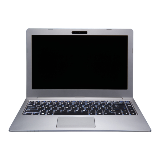
Page 16: External Locator - Top View With Lcd Panel Open
Introduction External Locator - Top View with LCD Panel Open Figure 1 Top View 1. PC Camera 2. *PC Camera LED *When the PC camera is in use, the LED will be illuminated in red. 3. Built-In Microphone 4. LCD 5. -
Page 17: External Locator - Front & Right Side Views
Introduction External Locator - Front & Right Side Views Figure 2 Front View 1. LED Indicator FRONT VIEW Figure 3 Right Side View 1. USB 3.0/3.1 Type- C Port (Factory Option) RIGHT SIDE VIEW Thunderbolt 3 Combo Port (Type- 2. USB 3.0/3.1 Type- A Port 3. -
Page 18: External Locator - Left Side & Rear View
Introduction External Locator - Left Side & Rear View Figure 4 Left Side View 1. DC-In Jack 2. USIM Card Reader (for 3G/4G LEFT SIDE VIEW USIM Cards) - Factory Option 3. USB 3.0/3.1 Type- A Port 4. Power Button 5. -
Page 19: External Locator - Bottom View
Introduction External Locator - Bottom View Figure 6 Bottom View 1. Vent 2. Speakers Overheating To prevent your com- puter from overhea- ting, make sure no- thing blocks any vent while the computer is in use. External Locator - Bottom View 1 - 7... -
Page 20: Mainboard Overview - Top (Key Parts)
Introduction Mainboard Overview - Top (Key Parts) Figure 7 Mainboard Top Key Parts 1 - 8 Mainboard Overview - Top (Key Parts) -
Page 21: Mainboard Overview - Bottom (Key Parts)
Introduction Mainboard Overview - Bottom (Key Parts) Figure 8 Mainboard Bottom Key Parts 1. CPU 2. Memory Slots DDR4 SO-DIMM 3. KBC-ITE IT8587 Mainboard Overview - Bottom (Key Parts) 1 - 9... -
Page 22: Mainboard Overview - Top (Connectors)
Introduction Mainboard Overview - Top (Connectors) Figure 9 Mainboard Top Connectors 1. USB Board Connector 2. Keyboard Cable Connector 3. White LED Keyboard Connector 4. RJ-45 LAN Jack 5. HDMI-Out Port 6. Mini Display Port 7. USB Port 3.0/3.1 Type A Port 8. -
Page 23: Mainboard Overview - Bottom (Connectors)
Introduction Mainboard Overview - Bottom (Connectors) Figure 10 Mainboard Bottom Connectors 1. Multi-in-1 Card Reader 2. Fan Connector 3. LCD Cable Connector 4. Speaker Connector 5. HDD Connector 6. Battery Connector 7. M.2 Card Connector (SSD) 8. 3G/4G Connector 9. WLAN Connector 10. - Page 24 Introduction 1 - 12...
-
Page 25: Disassembly
Chapter 2: Disassembly Overview This chapter provides step-by-step instructions for disassembling the N130BU / N131BU series notebook’s parts and subsystems. When it comes to reassembly, reverse the procedures (unless otherwise indicated). We suggest you completely review any procedure before you take the computer apart. -
Page 26: Maintenance Tools
Disassembly NOTE: All disassembly procedures assume that the system is turned OFF, and disconnected from any power supply (the battery is removed too). Maintenance Tools The following tools are recommended when working on the notebook PC: • M3 Philips-head screwdriver •... -
Page 27: Maintenance Precautions
Disassembly Maintenance Precautions The following precautions are a reminder. To avoid personal injury or damage to the computer while performing a re- moval and/or replacement job, take the following precautions: Power Safety Warning 1. Don't drop it. Perform your repairs and/or upgrades on a stable surface. If the computer falls, the case and other Before you undertake components could be damaged. -
Page 28: Disassembly Steps
Disassembly Disassembly Steps The following table lists the disassembly steps, and on which page to find the related information. PLEASE PERFORM THE DISASSEMBLY STEPS IN THE ORDER INDICATED. To remove the Keyboard: To remove and install the M.2 SSD Module: 1. -
Page 29: Removing The Keyboard
Disassembly Removing the Keyboard Figure 1 1. Turn off the computer, turn it over. Keyboard Removal 2. Remove screws from the bottom case (Figure 1a). 3. Open it up with the LCD on a flat surface before pressing at point to release the keyboard module (use the spe- cific eject stick to do this) while releasing the keyboard in the direction of the arrow... -
Page 30: Removing The Battery
Disassembly Removing the Battery Figure 2 Battery Removal 1. Turn off the computer, turn it over to remove the keyboard (page 2 - 2. Remove screws (Figure 2a). a. Remove the screws. 3. Remove screws on the bottom case (Figure 2b). -
Page 31: Removing The Hard Disk Drive
Disassembly Removing the Hard Disk Drive Figure 3 HDD Assembly The hard disk drive can be taken out to accommodate other 2.5" serial (SATA) hard disk drives with a height of 7.0mm Removal (h). Follow your operating system’s installation instructions, and install all necessary drivers and utilities (as outlined in Chapter 4 of the User’s Manual) when setting up a new hard disk. - Page 32 Disassembly 4. Slightly lift to pull the hard disk assembly in the direction of arrow (Figure 4c Figure 4 5. Lift the hard disk out of the bay (Figure 4d HDD Assembly 6. Reverse the process to install a new hard disk (do not forget to replace all the screws and bottom cover). Removal (cont’d.) c.
-
Page 33: Removing The System Memory (Ram)
Disassembly Removing the System Memory (RAM) Figure 5 RAM Module The computer has two memory sockets for 260 pin Small Outline Dual In-line Memory Modules (SO-DIMM) supporting Removal DDR4 2133MHz. The main memory can be expanded up to 32GB. The total memory size is automatically detected by the POST routine once you turn on your computer. - Page 34 Disassembly 5. Pull the latches to release the second module if necessary. 6. Insert a new module holding it at about a 30° angle and fit the connectors firmly into the memory slot. 7. The module will only fit one way as defined by its pin alignment. Make sure the module is seated as far into the slot as it will go.
-
Page 35: Removing The Wireless Lan Module
Disassembly Removing the Wireless LAN Module Figure 6 Wireless LAN 1. Turn off the computer, turn it over to remove the keyboard (page 2 - 5) and battery (page 2 - Module Removal 2. The Wireless LAN module will be visible at point on the mainboard (Figure 6a). -
Page 36: Wireless Lan, And Combo Module Cables
Disassembly Wireless LAN, and Combo Module Cables Note that the cables for connecting to the antennae on WLAN, WLAN & Bluetooth Combo, 3G and LTE modules are not labelled. The cables/covers (each cable will have either a black or transparent cable cover) are color coded for iden- tification as outlined in the table below. -
Page 37: Removing The 3G Module
Disassembly Removing the 3G Module Figure 7 3G Module Removal Procedure 3G Module Removal 1. Turn off the computer, turn it over to remove the keyboard (page 2 - 5) and battery (page 2 - a. Locate the module. 2. Locate the module, it is visible at point Figure 7a b. -
Page 38: Removing And Installing The M.2 Ssd Module
Disassembly Removing and Installing the M.2 SSD Module Figure 8 M.2 SSD-1 Module M.2 SSD-1 Removal Procedure Removal 1. Turn off the computer, turn it over to remove the keyboard (page 2 - 5) and battery (page 2 - 2. The M.2 SSD module will be visible at point on the mainboard (Figure 8a). - Page 39 Disassembly M.2 SSD-2 Removal Procedure Figure 9 1. Turn off the computer, turn it over to remove the keyboard (page 2 - 5) and battery (page 2 - M.2 SSD-2 Module 2. The M.2 SSD module will be visible at point on the mainboard (Figure 9a).
- Page 40 Disassembly M.2 SSD Installation Procedure Figure 10 M.2 SSD Module 1. Place the thermal pad on the module as shown (Figure 10a). Installation 2. Insert the module in the computer Figure 10b 3. Tighten the screw to secure the module in place (Figure 10c) a.
-
Page 41: Removing The Ccd
Disassembly Removing the CCD Figure 11 CCD Removal 1. Turn off the computer, turn it over to remove the keyboard (page 2 - 5) and battery (page 2 - 2. Run your fingers around the inner frame of the LCD panel at the points as indicated by the arrows (Figure a. - Page 42 Disassembly 4. Disconnect the cable (Figure 12f). Figure 12 5. Remove the CCD module (Figure 12g). CCD Removal 6. Reverse the process to install a new CCD module. (cont’d.) c. Disconnect the cable. d. Remove the CCD mod- ule. 6.
-
Page 43: Part Lists
Appendix A:Part Lists This appendix breaks down the N130BU / N131BU series notebook’s construction into a series of illustrations. The com- ponent part numbers are indicated in the tables opposite the drawings. Note: This section indicates the manufacturer’s part numbers. Your organization may use a different system, so be sure to cross-check any relevant documentation. -
Page 44: Part List Illustration Location
Part List Illustration Location The following table indicates where to find the appropriate part list illustration. Table A - 1 Part List Illustration Part Location page A - 3 Bottom page A - 4 page A - 5 page A - 6 A - 2... -
Page 45: Top
Figure A - 1 Top A - 3... -
Page 46: Bottom
Bottom Figure A - 2 Bottom A - 4 Bottom... -
Page 47: Lcd
Figure A - 3 LCD A - 5... - Page 48 Figure A - 4 A - 6 MB...
-
Page 49: Schematic Diagrams
Schematic Diagrams Appendix B: Schematic Diagrams This appendix has circuit diagrams of the N130BU / N131BU notebook’s PCB’s. The following table indicates where to find the appropriate schematic diagram. Diagram - Page Diagram - Page Diagram - Page Table B - 1... -
Page 50: System Block Diagram
Schematic Diagrams System Block Diagram 7 IN 1 6-7P-N1307-002 N130BU KABY LAKE U 2+2 (HDCP2.2) System Block Diagram MAIN BOARD SHEET 1~39 6-71-N1300-D02A USB BOARD 3V,5V,3VS,5VS,1.8VS 1866/ 2133 MHz 6-71-N1303-D02A SHEET 40 DDR4 SHEET 32 DDR4 AUDIO BOARD SO-DIMM A... - Page 51 [02] KBL1/10 DDR4 [02] KBL1/10 DDR4 Size Size Size Document Number Document Number Document Number 6-71-N1300-D02A 6-71-N1300-D02A 6-71-N1300-D02A N130BU N130BU N130BU 2.0A 2.0A 2.0A Date: Date: Date: W ednesday, November 30, 2016 W ednesday, November 30, 2016 W ednesday, November 30, 2016...
- Page 52 [03] KBL 2/10 DISPLAY [03] KBL 2/10 DISPLAY Size Size Size Document Number Document Number Document Number 6-71-N1300-D02A 6-71-N1300-D02A 6-71-N1300-D02A N130BU N130BU N130BU 2.0A 2.0A 2.0A Date: Date: Date: W ednesday, November 30, 2016 W ednesday, November 30, 2016 W ednesday, November 30, 2016...
-
Page 53: Processor 3/10
[04] KBL 3/10 SATA/PCIE/USB [04] KBL 3/10 SATA/PCIE/USB Size Size Size Document Number Document Number Document Number 6-71-N1300-D02A 6-71-N1300-D02A 6-71-N1300-D02A N130BU N130BU N130BU 2.0A 2.0A 2.0A Date: Date: Date: W ednesday, November 30, 2016 W ednesday, November 30, 2016 W ednesday, November 30, 2016... - Page 54 1.0VS 6,7,10,24,26,27,29,32,33,34,35,37,39 VDD3 Size Size Size Document Number Document Number Document Number 6-71-N1300-D02A 6-71-N1300-D02A 6-71-N1300-D02A RTCVCC N130BU N130BU N130BU 2.0A 2.0A 2.0A 3,4,6,7,12,13,14,15,16,17,18,20,24,25,26,27,28,29,30,31,32,38 3.3VS Date: Date: Date: W ednesday, November 30, 2016 W ednesday, November 30, 2016 W ednesday, November 30, 2016...
-
Page 55: Processor 5/10
PM_PW ROK PCH_HDA_SPKR R399 *1K_04 Size Size Size Document Number Document Number Document Number 74LVC08APW 6-71-N1300-D02A 6-71-N1300-D02A 6-71-N1300-D02A N130BU N130BU N130BU 2.0A 2.0A 2.0A Date: Date: Date: Friday, December 02, 2016 Friday, December 02, 2016 Friday, December 02, 2016 Sheet Sheet... - Page 56 VDD3 Size Size Size Document Number Document Number Document Number 6-71-N1300-D02A 6-71-N1300-D02A 6-71-N1300-D02A MTDK3S6R 4,6,10,32 3.3VA SMB_DATA N130BU N130BU N130BU SMB_DAT_DDR 12,13 2.0A 2.0A 2.0A 3,4,5,6,12,13,14,15,16,17,18,20,24,25,26,27,28,29,30,31,32,38 3.3VS Date: Date: Date: W ednesday, November 30, 2016 W ednesday, November 30, 2016...
-
Page 57: Processor 7/10
[08] KBL 7/11 RESERVED SIGNALS [08] KBL 7/11 RESERVED SIGNALS Size Size Size Document Number Document Number Document Number 6-71-N1300-D02A 6-71-N1300-D02A 6-71-N1300-D02A N130BU N130BU N130BU 2.0A 2.0A 2.0A Date: Date: Date: W ednesday, November 30, 2016 W ednesday, November 30, 2016... - Page 58 KBL_ULT REV = 1 Size Size Size Document Number Document Number Document Number 6-71-N1300-D02A 6-71-N1300-D02A 6-71-N1300-D02A N130BU N130BU N130BU 2.0A 2.0A 2.0A Date: Date: Date: W ednesday, November 30, 2016 W ednesday, November 30, 2016 W ednesday, November 30, 2016...
-
Page 59: Processor 9/10
[10] KBL 9/11 POWER2 [10] KBL 9/11 POWER2 Size Size Size Document Number Document Number Document Number 6-71-N1300-D02A 6-71-N1300-D02A 6-71-N1300-D02A N130BU N130BU N130BU 2.0A 2.0A 2.0A Date: Date: Date: W ednesday, November 30, 2016 W ednesday, November 30, 2016 W ednesday, November 30, 2016... - Page 60 [11] KBL 10/11 POWER3,VSS [11] KBL 10/11 POWER3,VSS [11] KBL 10/11 POWER3,VSS Size Size Size Document Number Document Number Document Number 6-71-N1300-D02A 6-71-N1300-D02A 6-71-N1300-D02A N130BU N130BU N130BU 2.0A 2.0A 2.0A 36,38 VCCGT Date: Date: Date: W ednesday, November 30, 2016...
-
Page 61: Ddr4 So-Dimm_0
[12] DDR4 SO-DIMM_0 24.9_1%_04 VREFCA_CHA_DIMM Size Size Size Document Number Document Number Document Number 6-71-N1300-D02A 6-71-N1300-D02A 6-71-N1300-D02A N130BU N130BU N130BU 2.0A 2.0A 2.0A Date: Date: Date: W ednesday, November 30, 2016 W ednesday, November 30, 2016 W ednesday, November 30, 2016... -
Page 62: Ddr4 So-Dimm_1
[13] DDR4 SO-DIMM_1 24.9_1%_04 VREFCA_CHB_DIMM Size Size Size Document Number Document Number Document Number 6-71-N1300-D02A 6-71-N1300-D02A 6-71-N1300-D02A N130BU N130BU N130BU 2.0A 2.0A 2.0A Date: Date: Date: W ednesday, November 30, 2016 W ednesday, November 30, 2016 W ednesday, November 30, 2016... -
Page 63: Hdmi
[14] HDMI [14] HDMI Size Size Size Document Number Document Number Document Number 6-71-N1300-D02A 6-71-N1300-D02A 6-71-N1300-D02A N130BU N130BU N130BU 2.0A 2.0A 2.0A Date: Date: Date: W ednesday, November 30, 2016 W ednesday, November 30, 2016 W ednesday, November 30, 2016... -
Page 64: Panel
[15] PANEL 26,32,33,34,35,36,37,38,39 Size Size Size Document Number Document Number Document Number 6-71-N1300-D02A 6-71-N1300-D02A 6-71-N1300-D02A 3,4,5,6,7,12,13,14,16,17,18,20,24,25,26,27,28,29,30,31,32,38 3.3VS N130BU N130BU N130BU 2.0A 2.0A 2.0A 3,6,20,22,27,30,31,32,34,35,37 3.3V Date: Date: Date: Friday, December 02, 2016 Friday, December 02, 2016 Friday, December 02, 2016... -
Page 65: Rtd2136N
Schematic Diagrams RTD2136N VCCK_V12 LVDS Power LVDS 3.3VS AVCC33 3.3VS DVCC33 :33pcs R496 0_06 LVDS R283 0_06 LVDS C309 LVDS 40mils 40mils C528 80mils 80mils 0.1u_10V_X7R_04 C527 LVDS C340 C312 ENBLT ENBLT LVDS LVDS LVDS 0.1u_10V_X7R_04 2.2u_6.3V_X5R_04 2.2u_6.3V_X5R_04 0.1u_10V_X7R_04 R249 LVDS 10K_04 LVDS... -
Page 66: Ps8338B
Title [17] PS8338B [17] PS8338B [17] PS8338B Size Size Size Document Number Document Number Document Number 6-71-N1300-D02A 6-71-N1300-D02A 6-71-N1300-D02A N130BU N130BU N130BU 2.0A 2.0A 2.0A 3,4,5,6,7,12,13,14,15,16,18,20,24,25,26,27,28,29,30,31,32,38 3.3VS Date: Date: Date: W ednesday, November 30, 2016 W ednesday, November 30, 2016... -
Page 67: Minidp
W /O-TBT Size Size Size Document Number Document Number Document Number 6-71-N1300-D02A 6-71-N1300-D02A 6-71-N1300-D02A 3,4,5,6,7,12,13,14,15,16,17,20,24,25,26,27,28,29,30,31,32,38 3.3VS N130BU N130BU N130BU 2.0A 2.0A 2.0A 14,25,29,31,32 Date: Date: Date: W ednesday, November 30, 2016 W ednesday, November 30, 2016 W ednesday, November 30, 2016... -
Page 68: Ar_Tbt
Document Number Document Number 6-71-N1300-D02A 6-71-N1300-D02A 6-71-N1300-D02A 20,21 VCC3V3_SX_SYS 2.0A 2.0A 2.0A Custom Custom Custom N130BU N130BU N130BU Date: Date: Date: Wednesday, December 21, 2016 Wednesday, December 21, 2016 Wednesday, December 21, 2016 Sheet Sheet Sheet B - 20 AR_TBT... -
Page 69: Ar_Power
Size Size Size Document Number Document Number Document Number 6-71-N1300-D02A 6-71-N1300-D02A 6-71-N1300-D02A 2.0A 2.0A 2.0A N130BU N130BU N130BU Date: Date: Sheet Sheet Date: W ednesday, December 21, 2016 W ednesday, December 21, 2016 W ednesday, December 21, 2016 Sheet AR_Power B - 21... -
Page 70: Tps65982
Size Size Document Number Document Number Document Number 6-71-N1300-D02A 6-71-N1300-D02A 6-71-N1300-D02A 2.0A 2.0A 2.0A 22,29,31,32,34,37,38 N130BU N130BU N130BU Date: Date: Date: W ednesday, November 30, 2016 W ednesday, November 30, 2016 W ednesday, November 30, 2016 Sheet Sheet Sheet B - 22 TPS65982... -
Page 71: Asm1543
[22] ASM1543 [22] ASM1543 Size Size Size Document Number Document Number Document Number 6-71-N1300-D02A 6-71-N1300-D02A 6-71-N1300-D02A N130BU N130BU N130BU 2.0A 2.0A 2.0A Date: Date: Date: W ednesday, November 30, 2016 W ednesday, November 30, 2016 W ednesday, November 30, 2016... -
Page 72: Type C
0_04 W /TBT TBTA_USB2_BP Size Size Size Document Number Document Number Document Number 6-71-N1300-D02A 6-71-N1300-D02A 6-71-N1300-D02A N130BU N130BU N130BU 2.0A 2.0A 2.0A Date: Date: Date: W ednesday, November 30, 2016 W ednesday, November 30, 2016 W ednesday, November 30, 2016... -
Page 73: Card Reader & Lan_Rtl8411B
[24] CARD READER & LAN_RTL8411B MA1206CG-101J-202ER 6-07-1012C-HB0 Size Size Size Document Number Document Number Document Number 2.0A 2.0A 2.0A N130BU N130BU N130BU 6-71-N1300-D02A 6-71-N1300-D02A 6-71-N1300-D02A 6-07-1012C-1B0 Date: Date: Date: W ednesday, November 30, 2016 W ednesday, November 30, 2016 W ednesday, November 30, 2016... -
Page 74: Audio Codec
[25] ALC269Q-VC2(AUDIO CODEC) [25] ALC269Q-VC2(AUDIO CODEC) Size Size Size Document Number Document Number Document Number 6-71-N1300-D02A 6-71-N1300-D02A 6-71-N1300-D02A N130BU N130BU N130BU 2.0A 2.0A 2.0A Date: Date: Date: W ednesday, November 30, 2016 W ednesday, November 30, 2016 W ednesday, November 30, 2016... -
Page 75: Kbc Ite It8587
CCD_EN R325 *100K_04 LED_BAT_FULL PM_PW ROK 6,26 GPA6/PWM6/SSCK/5VT TMRI1/GPC6 10K_1% 3.3V LED_PW R GPA7/PWM7/RIG1#/5VT PS/2 10K_1% CTX0/TMA0/GPB2 LAN_W AKEUP# 6,24,27 N130BU 80CLK W LAN_PW R_EN *100K_04 GPF0/PS2CLK0/TMB0/CEC/5VT 3IN1 22.6K_1% 10K_1% 1.01V GPF2/PS2CLK1/DTR0#/5VT 5VT/L80HLAT/BAO/GPE0 SW I# 10K_1% 15.4K_1% 32,33 USB_CHARGE_EN GPF1/PS2DAT0/TMB1/5VT... -
Page 76: Wlan/Bt, 3G
GND0 Size Size Size Document Number Document Number Document Number 6-71-N1300-D02A 6-71-N1300-D02A 6-71-N1300-D02A 2.0A 2.0A 2.0A N130BU N130BU N130BU 213AAAA32FA P/N = 6-21-84KV0-075 Date: Date: Date: Friday, December 02, 2016 Friday, December 02, 2016 Friday, December 02, 2016 Sheet Sheet... -
Page 77: M Key Pcie Ssd
Size Size Size Document Number Document Number Document Number 6-71-N1300-D02A 6-71-N1300-D02A 6-71-N1300-D02A 2.0A 2.0A 2.0A N130BU N130BU N130BU Date: Date: Date: W ednesday, November 30, 2016 W ednesday, November 30, 2016 W ednesday, November 30, 2016 Sheet Sheet Sheet M Key PCIE SSD B - 29... -
Page 78: Sata, Led, Lid, Sw
P/N = 6-02-08251-LC0 3,4,5,6,7,12,13,14,15,16,17,18,20,24,25,26,27,28,30,31,32,38 3.3VS Size Size Size Document Number Document Number Document Number 21,22,31,32,34,37,38 6-71-N1300-D02A 6-71-N1300-D02A 6-71-N1300-D02A N130BU N130BU N130BU 2.0A 2.0A 2.0A Date: Date: Date: Friday, December 02, 2016 Friday, December 02, 2016 Friday, December 02, 2016 Sheet... -
Page 79: Usb / Tpm
Schematic Diagrams USB / TPM USB PORT Charge USB 3.0 port (CHARGER) USB3.0 Max Trace length C582 22u_6.3V_X5R_08 C540 22u_6.3V_X5R_08 Follow Design Guide 80 MIL Smart CDP C524 *22u_6.3V_X5R_08 USBVCC_CH C525 *22u_6.3V_X5R_08 pin8 pin4 Function 0822 22uX2 CLOSE TO CONNECTOR J_USB3_1 DCP autodetect with TVUDF1004AD0... -
Page 80: Conn, Ccd, Fan, Tp, Led Kb
[31] CONN,CCD,FAN,T/P,LEDKB [31] CONN,CCD,FAN,T/P,LEDKB Solution) Size Size Size Document Number Document Number Document Number 6-71-N1300-D02A 6-71-N1300-D02A 6-71-N1300-D02A CONNECT N130BU N130BU N130BU 2.0A 2.0A 2.0A Date: Date: Date: Friday, December 02, 2016 Friday, December 02, 2016 Friday, December 02, 2016 Sheet... -
Page 81: 5V, 3Vs, 5Vs, 1.8Vs Ctl
[32] 3V,5V,3VS,5VS,1.8VS CTL [32] 3V,5V,3VS,5VS,1.8VS CTL Size Size Size Document Number Document Number Document Number 2.0A 2.0A 2.0A N130BU N130BU N130BU 6-71-N1300-D02A 6-71-N1300-D02A 6-71-N1300-D02A Date: Date: Date: W ednesday, November 30, 2016 W ednesday, November 30, 2016 W ednesday, November 30, 2016... -
Page 82: Vdd3, Vdd5
Schematic Diagrams VDD3, VDD5 VREF_VDD PR70 0_04 PC59 1u_6.3V_X5R_04 PR182 PR183 PC55 EN_3V EN_5V 1000p_50V_X7R_04 130K_1%_04 130K_1%_04 PC48 0824 08 COLAY B2 PC138 PC156 PC58 1000p_50V_X7R_04 B2 08 Size Colay VREG3 PC57 PC155 PC139 PC153 PC159 PC46 VCC_3P3DSW _PW RGD 1u_6.3V_X5R_04 PR67 *10K_04... -
Page 83: Vddq, Vddq_Vtt, 1.5Vs, 1.8Va
Title Title Title [34] VDDQ,VDDQ_VTT,1.5VS,1.8VA [34] VDDQ,VDDQ_VTT,1.5VS,1.8VA [34] VDDQ,VDDQ_VTT,1.5VS,1.8VA 10K_1%_04 Size Size Size Document Number Document Number Document Number N130BU N130BU N130BU 2.0A 2.0A 2.0A 6-71-N1300-D02A 6-71-N1300-D02A 6-71-N1300-D02A Date: Date: Date: W ednesday, November 30, 2016 W ednesday, November 30, 2016... -
Page 84: Series
5,6,7,10,24,26,27,29,32,33,34,37,39 VDD3 3,6,15,20,22,27,30,31,32,34,37 3.3V Size Size Size Document Number Document Number Document Number 15,26,32,33,34,36,37,38,39 2.0A 2.0A 2.0A N130BU N130BU N130BU 6-71-N1300-D02A 6-71-N1300-D02A 6-71-N1300-D02A 33,34 VDD5_LDO5 Date: Date: Date: Thursday, December 01, 2016 Thursday, December 01, 2016 Thursday, December 01, 2016... -
Page 85: Vccgt, Vccsa
[36] ,VCCGT,VCCSA [36] ,VCCGT,VCCSA Size Size Size Document Number Document Number Document Number 2.0A 2.0A 2.0A N130BU N130BU N130BU 6-71-N1300-D02A 6-71-N1300-D02A 6-71-N1300-D02A Date: Date: Date: W ednesday, November 30, 2016 W ednesday, November 30, 2016 W ednesday, November 30, 2016... -
Page 86: V, Vccio_Out, Vccin
[37] 2.5V,VCCIO-OUT,VCCIN AVcore1 LL/IMON Compesation Size Size Size Document Number Document Number Document Number 2.0A 2.0A 2.0A N130BU N130BU N130BU 6-71-N1300-D02A 6-71-N1300-D02A 6-71-N1300-D02A Date: Date: Date: W ednesday, November 30, 2016 W ednesday, November 30, 2016 W ednesday, November 30, 2016... -
Page 87: Rt3601Bc
NOT use driver. ISEN2N_GT Pin need pull up 5V? Title Title Title [38] RT3601BC [38] RT3601BC [38] RT3601BC Size Size Size Document Number Document Number Document Number N130BU N130BU N130BU 6-71-N1300-D02A 6-71-N1300-D02A 6-71-N1300-D02A 2.0A 2.0A 2.0A Date: Date: Date: Wednesday, November 30, 2016... -
Page 88: Charger, Dc In
[39] CHARGER,DC IN Size Size Size Document Number Document Number Document Number 2.0A 2.0A 2.0A Custom Custom Custom N130BU N130BU N130BU 6-71-N1300-D02A 6-71-N1300-D02A 6-71-N1300-D02A Date: Date: Date: Friday, December 09, 2016 Friday, December 09, 2016 Friday, December 09, 2016 Sheet... -
Page 89: Usb Board
Schematic Diagrams USB Board Z3.3V USB3.0 PORT4 ZUSBVCC 100 MIL VOUT 0.01u_16V_X7R_04 0.1u_10V_X7R_04 1u_6.3V_X5R_04 ZC12 ZC13 Z3.3V 10u_6.3V_X5R_06 0.1u_16V_Y5V_04 *0_04 2K_1%_04 *4.7K_04 ZGND *4.7K_04 ZGND uP7549UMA5-20 ZGND PCB Footprint = M-SOT23-5 ZGND 2A/90mohm ZGND ASM1464 ZDD_ON# ZR20 *0402_short Z_SCK_P4 Z_SDA_P4 *4.7K_04 *4.7K_04 NEW PART... - Page 90 0.1u_16V_Y5V_04 [41] AUDIO BOARD [41] AUDIO BOARD [41] AUDIO BOARD 0.1u_16V_Y5V_04 Size Size Size Document Number Document Number Document Number 6-71-N1308-D02A 6-71-N1308-D02A 6-71-N1308-D02A N130BU N130BU N130BU 2.0A 2.0A 2.0A A_AUDG A_AUDG A_AUDG A_AUDG Date: Date: Date: Wednesday, November 30, 2016...
-
Page 91: Click Board
Schematic Diagrams Click Board CLICK BOARD To T/P To M/B CJ_TP1 CTP_VCC CTP_CLK_J CTP_CLK CJ_MB1 CTP_DATA_J CTP_DATA CTP_SMB_CLK CTPBUTTON_L CTP_SMB_DATA 20mil CGND CGND 20mil CTPBUTTON_R CTP_SMB_CLK CGND CTP_SMB_DATA CTP_CLK CTP_SMB_CLK_J CTP_DATA CTP_SMB_DATA_J CTP_VCC ONLY 3.3V FP225H-008S11M FP225H-006S10M *TVUDF1004AD0 fp225h-008gxxxm PCB Footprint = fp225h-006xxxm P/N = 6-20-94K30-108 P/N = 6-20-94K00-006 0.1u_10V_X7R_04... -
Page 92: Led Board
Schematic Diagrams LED Board LED BOARD LGND L_LED_ACIN L_LED_BAT_FULL L_LED_PWR L_LED_BAT_CHG L3.3VS LJ_LED1 *TVUDF1004AD0 NC 2pin, L_LED_BAT_CHG L_LED_BAT_FULL L_LED_ACIN L_LED_PWR L_LED_HDD# L_AIRPLAN_LED# LGND Sheet 43 of 45 220_04 220_04 220_04 0817 FP225H-010S10M 220_04 *V15AVLC0402 FP225H-010-xxxM LGND LGND LED Board RY-SP155HYYG4-1 RY-SP155HYYG4-1 POWER ON LED/ AC IN FULL LED/ BAT CHARGE... -
Page 93: Dc Jack Board
Schematic Diagrams DC Jack Board KJ_DC_JACK1 0824 PIN Change KJ_DC_IN1 KVIN Sheet 44 of 45 50278-00201-001 GND1 DC Jack Board PCB Footprint = 50278-002xx-xxx_l GND2 P/N = 6-21-63100-002 TDC-090HR2-H-005-1AG PCB Footprint = DC090H-005-P KGND P/N = 6-20-B3Y00-004 *H7_0D2_3 *H6_0D2_3 *H5_0D2_2 *H5_0D2_2 H7_0D2_3 H6_0D2_3... -
Page 94: Dc Jack Board_W
Schematic Diagrams DC Jack Board_W 0824 PIN Change WJ_DC_JACK1 WJ_DC_IN1 WVIN Sheet 45 of 45 DC Jack Board_W 50278-00201-001 GND1 PCB Footprint = 50278-002xx-xxx_l GND2 P/N = 6-21-63100-002 TDC-090HR2-H-005-1AG PCB Footprint = DC090H-005-P WGND P/N = 6-20-B3Y00-004 *H6_0D2_3 *H6_0D2_3 *H3_5B1_5D1_5 *H5_0D2_2 H6_0D2_3 H6_0D2_3... -
Page 95: Updating The Flash Rom Bios
Download the BIOS computer model. 1. Go to www.clevo.com.tw and point to E-Services and click E-Channel. Note that BIOS versions 2. Use your user ID and password to access the appropriate download area (BIOS), and download the latest BIOS files... -
Page 96: Use The Flash Tools To Update The Bios
BIOS Update Use the flash tools to update the BIOS 1. Make sure you are not loading any memory management programs such as HIMEM by holding the F8 key as you see the message “EFI Shell”. You will then be prompted to give “Y” or “N” responses to the programs being loaded by EFI Shell.