Bose FreeSpace 4400 Service Manual
Hide thumbs
Also See for FreeSpace 4400:
- Owner's manual (70 pages) ,
- Installation manual (12 pages) ,
- Manual (20 pages)

Related Manuals for Bose FreeSpace 4400


Summary of Contents for Bose FreeSpace 4400
- Page 1 ® FreeSpace 4400 Business Music System ©2008 Bose Corporation Service Manual Reference Number 294963-SM Rev. 00 Electronic Copy Only...
-
Page 2: Table Of Contents
® Packaging Part List, FreeSpace 4400 System ................13 Figure 1. FreeSpace 4400 System Packaging View .................13 Packaging Part List, Rack Ear / Connector Kit ................14 Figure 2. Rack Ear / Connector Kit Packaging View ................14 Main Part List, FreeSpace Model 4400 Amplifier ..............15-16 Figure 3. -
Page 3: Safety Information
THIS DOCUMENT CONTAINS PROPRIETARY INFORMATION OF BOSE CORPORATION WHICH IS BEING FURNISHED ONLY FOR THE PURPOSE OF SERVICING THE IDENTIFIED BOSE PRODUCT BY AN AUTHORIZED BOSE SERVICE CENTER OR OWNER OF THE BOSE PRODUCT, AND SHALL NOT BE REPRODUCED OR USED FOR ANY OTHER PURPOSE. -
Page 4: Warranty
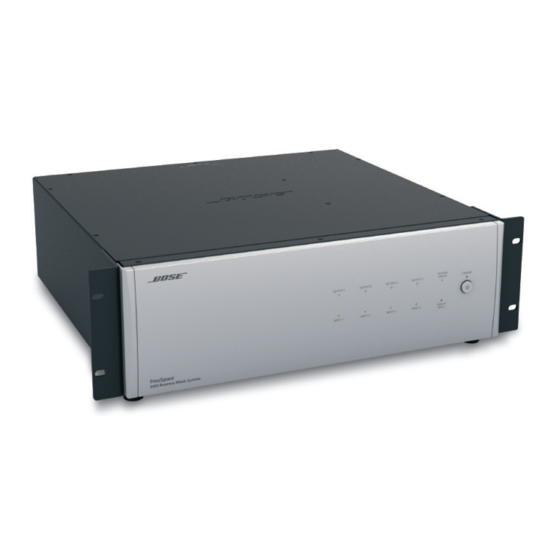
400-Watt power amplifier for 70/100V business music applications. The FreeSpace 4400 chassis provides a total of four source inputs (two Line In, one Mic/Line and one Mic/Line/Page) to meet the needs of most business music installations. A Music on Hold (MOH) output is also provided for simple integration into a phone system. -
Page 5: Specifications
SPECIFICATIONS Audio Input Source 1 Unbalanced RCA, shell grounded through a 301 Ohm resistor Connectors: Source 2 Unbalanced RCA, shell grounded through a 301 Ohm resistor Page Balanced 4 pin Beau style: +, -, ground and contact closure in Aux/Mic/Line 3 pin Beau style, +, - and ground Mic 1-4 3 pin Beau style, +, - and ground Direct In... - Page 6 SPECIFICATIONS Line Input Source 1 and 2 Nominal Limits Conditions Source impedance: 200 Ohms 10 to 2k Ohm Frequency response specification maintained with sources over this range Input impedance differential: +/> 50k Ohm +/-20% At 1 kHz CMRR referred to 80 dB >/= 74 dB At 1 kHz, 20 dB gain, 200 Ohm source...
- Page 7 SPECIFICATIONS Page and Aux/Mic Inputs (continued) Nominal Limits Conditions CMRR referred 90 dB >/= 70 dB At 1 kHz, 60 dB gain, from source of nominal to output: 200 Ohms Input sensitivity for -60 dBV to +/-1 dB At 1 kHz codec FS: +17 dBV Gain, all settings:...
- Page 8 SPECIFICATIONS Sense Mic inputs (continued) Nominal Limits Conditions Maximum input level: +10 dBV >/= 7 dBV THD+N </= 0.3%, 20-20 kHz, 0 dB gain THD+N: -84 dB </= -80 dB At +10 dBV output, 1 kHz, 60 dB gain Crosstalk at 1 kHz: -90 dB </= -80 dB Crossalk at 10 kHz:...
- Page 9 SPECIFICATIONS Line Outputs (continued) Nominal Limits Conditions CMRR referred to output: 92 dB >/= 60 dB At 1 kHz, 20 dB gain, 200 Ohm source impedance Output noise: -90 dBV </= -85 dBV A-weighted, set for 0 dB gain THD+N: .001% .01% At +10 dBV output, 1 kHz, 20 dB gain...
- Page 10 SPECIFICATIONS Power Amplifier Nominal Limits Conditions Power bandwidth: 30 Hz to 1% THD Loaded at 25 Ohms 20 kHz Frequency response: 30 Hz to +/-3 dB Output voltage of 10 Vrms over a load 20 kHz impedance of 12.5 Ohms to 1000 Ohms THD+N at 70.7 Vrms, .05% 30 Hz to 20 kHz, 25 Ohm load, A weighted...
-
Page 11: Electrostatic Discharge Sensitive (Esds) Device Handling
PRODUCT VARIATIONS ® Description Bose Product Code ® FREESPACE 4400 AMPLIFIER, 120V, US/CAN 042346 FREESPACE 4400 AMPLIFIER, 230V, EURO 042347 FREESPACE 4400 AMPLIFIER, 100V, JAPAN 042348 FREESPACE 4400 AMPLIFIER, 230V, UK 042349 FREESPACE 4400 AMPLIFIER, 240V, AUS 042350... -
Page 12: Accessories
ACCESSORIES ® ® Optional Bose accessories for the FreeSpace 4400 system are available. • FreeSpace 4400 System AVM 1-Zone FreeSpace ® AVM 1-Zone User Interface User Interface (PC 042351) A wall-mount- able keypad that fits into a standard double- Select LINE 1 Volume up gang junction box. -
Page 13: 4400 System
POLY BAG, 10x14’ 1497-4122+0 DOCUMENT PACK, INCLUDES: 302390 SVC-EXPO11+DOC MANUAL 301433 4301-7264+0 POLYBAG FOR MANUAL 1497-1062+0 FS 4400 SOFTWARE CD 301428-001 4115-0005+0 QUICKSTART GUIDE 301434 3050-4011+0 POLYBAG FOR UNIT 1497-8012+0 FREESPACE 4400 AMPLIFIER Figure 1. FreeSpace 4400 System Packaging View... -
Page 14: Packaging Part List, Rack Ear / Connector Kit
PACKAGING PART LIST Rack Ear / Connector Kit (see Figure 2) ® Item Description Bose Part Vendor Part Number Qty. Note Number Number ACCESSORY KIT, INCLUDES: 302389 SVC-EXPO11+KIT CARTON 1481-0500+0 POLYBAG, 04x5x9’ 1497-1932+0 BRACKET, RACK EAR 4135-6501+0 LABEL, VOLTAGE SELECT... -
Page 15: Main Part List, Freespace Model 4400 Amplifier
MAIN PART LIST FreeSpace ® Model 4400 Amplifier (see Figure 3) ® Item Description Bose Part Vendor Part Number Qty. Note Number Number CHASSIS 1406-0301+0 3, 4 SCREW, SELF TAPPING 2941-3006+3000 SCREW, PAN, VOLT SEL CVR 2900-3006+3200 COVER, AC SELECT SWITCH... - Page 16 MAIN PART LIST FreeSpace ® Model 4400 Amplifier (continued) (see Figure 3) ® Item Description Bose Part Vendor Part Number Qty. Note Number Number MAIN DSP PCB ASSY 301398 SVC-EXPO01+DSPJ WALL PLATE PCB ASSY 301400 SVC-EXPO01+WALLP MIC SENSE PCB ASSY...
-
Page 17: Electrical Part Lists
ELECTRICAL PART LIST Front Panel PCB Assembly Resistors Reference Description Vendor Part Note Designator Number R101 1.1K, RMG, 0805, 1/10W, 1% 4720-112A+J R102 10K, RMG, 0805, 1/10W, 1% 4720-103A+J R107 10 OHM, RMG, 2512, 1W, 5% 4728-100J+3 R108 562 OHM, RMG, 0805, 1/10W, 1% 4720-5620+J R109 562 OHM, RMG, 0805, 1/10W, 1%... - Page 18 ELECTRICAL PART LIST Front Panel PCB Assembly Diodes Reference Description Vendor Part Note Designator Number D102 1N4148W, SOD-123, SMD, PANJIT 4801-48W0+3 D103 S1A, 1A, 50V, DO-214AA, SMD, PANJIT 480S-1A00+3 Integrated Circuits Reference Description Vendor Part Note Designator Number U101 SN74HC14D, SOP PACKAGE 3130-8680+0 U102 8 BIT SHIFT REG, M74HC595M1R, SO16, ST...
-
Page 19: Digital Signal Processor Pcb Assembly
ELECTRICAL PART LIST Digital Signal Processor PCB Assembly Resistors Reference Description Vendor Part Note Designator Number R501 18.2K, RMG, 1/10W, 1%, 0805 4720-1822+J R502 182 OHM, RMG, 1/10W, 1%, 0805 4720-1820+J R503 5.11K, RMG, 1/10W, 1%, 0805 4720-5111+J R504 7.87K, RMG, 1/10W, 1%, 0805 4720-7871+J R505 1.27K, RMG, 1/10W, 1%, 0805... - Page 20 ELECTRICAL PART LIST Digital Signal Processor PCB Assembly Resistors (continued) Reference Description Vendor Part Note Designator Number R555 7.87K, RMG, 1/10W, 1%, 0805 4720-7871+J R556 5.11K, RMG, 1/10W, 1%, 0805 4720-5111+J R557 5.11K, RMG, 1/10W, 1%, 0805 4720-5111+J R558 18.2K, RMG, 1/10W, 1%, 0805 4720-1822+J R561 4.75K, RMG, 1/10W, 1%, 0805...
- Page 21 ELECTRICAL PART LIST Digital Signal Processor PCB Assembly Resistors (continued) Reference Description Vendor Part Note Designator Number R624 1M, RMG, 1/10W, 1%, 0805 4720-105A+J R625 1M, RMG, 1/10W, 1%, 0805 4720-105A+J R626 1M, RMG, 1/10W, 1%, 0805 4720-105A+J R627 1M, RMG, 1/10W, 1%, 0805 4720-105A+J R628 1K, RMG, 1/10W, 1%, 0805...
- Page 22 ELECTRICAL PART LIST Digital Signal Processor PCB Assembly Resistors (continued) Reference Description Vendor Part Note Designator Number R683 2K, RMG, 1/10W, 1%, 0805 4720-202A+J R684 100K, RMG, 1/10W, 1%, 0805 4720-104A+J R685 100K, RMG, 1/10W, 1%, 0805 4720-104A+J R686 100K, RMG, 1/10W, 1%, 0805 4720-104A+J R687 2K, RMG, 1/10W, 1%, 0805...
- Page 23 ELECTRICAL PART LIST Digital Signal Processor PCB Assembly Resistors (continued) Reference Description Vendor Part Note Designator Number R736 11K, RMG, 1/10W, 1%, 0805 4720-113A+J R737 49.9K, RMG, 1/10W, 1%, 0805 4720-4992+J R738 15K, RMG, 1/10W, 1%, 0805 4720-153A+J R739 15K, RMG, 1/10W, 1%, 0805 4720-153A+J R740 22.1K, RMG, 1/10W, 1%, 0805...
- Page 24 ELECTRICAL PART LIST Digital Signal Processor PCB Assembly Resistors (continued) Reference Description Vendor Part Note Designator Number R792 100 OHM, RMG, 1/10W, 1%, 0805 4720-101A+J R793 267 OHM, RMG, 1/10W, 1%, 0805 4720-2670+J R794 10K, RMG, 1/10W, 1%, 0805 4720-103A+J Capacitors Reference Description...
- Page 25 ELECTRICAL PART LIST Digital Signal Processor PCB Assembly Capacitors (continued) Reference Description Vendor Part Note Designator Number C545 0.1uF, CC, 25V, 10%, 0805, 1.2x2.0 150E-104K+J-BD C547 0.1uF, CC, 25V, 10%, 0805, 1.2x2.0 150E-104K+J-BD C548 0.1uF, CC, 25V, 10%, 0805, 1.2x2.0 150E-104K+J-BD C551 1000pF, CC, 50V, 5%, 0805, 1.25X2.0...
- Page 26 ELECTRICAL PART LIST Digital Signal Processor PCB Assembly Capacitors (continued) Reference Description Vendor Part Note Designator Number C597 1000pF, CC, 50V, 5%, 0805, 1.25X2.0 150F-102J+J-BDM C598 2.2uF, CE, 35V, 20%, SMD, 3X5.4, 157Q-225M+3-EJC UWX1V2R2MCR2GB, NCC C599 2.2uF, CE, 35V, 20%, SMD, 3X5.4, 157Q-225M+3-EJC UWX1V2R2MCR2GB, NCC C601...
- Page 27 ELECTRICAL PART LIST Digital Signal Processor PCB Assembly Capacitors (continued) Reference Description Vendor Part Note Designator Number C648 0.1uF, CC, 25V, 10%, 0805, 1.2x2.0 150E-104K+J-BD C649 0.1uF, CC, 25V, 10%, 0805, 1.2x2.0 150E-104K+J-BD C650 0.1uF, CC, 25V, 10%, 0805, 1.2x2.0 150E-104K+J-BD C651 0.1uF, CC, 25V, 10%, 0805, 1.2x2.0...
- Page 28 ELECTRICAL PART LIST Digital Signal Processor PCB Assembly Capacitors (continued) Reference Description Vendor Part Note Designator Number C687 0.01uF, CC, 50V, 5%, 0805 150F-103J+J-BD C688 0.1uF, CC, 25V, 10%, 0805, 1.2x2.0 150E-104K+J-BD C689 0.33uF, CC, 16V, 5%, 0805 150D-334J+J-BD C690 0.1uF, CC, 25V, 10%, 0805, 1.2x2.0 150E-104K+J-BD C691...
- Page 29 ELECTRICAL PART LIST Digital Signal Processor PCB Assembly Capacitors (continued) Reference Description Vendor Part Note Designator Number C726 100uF, CE, 25V, 20%, 6.3X7.7, SMD, 157E-107M+3-LOC UWX1E101MCR1GB, NCC C727 0.1uF, CC, 25V, 10%, 0805, 1.2x2.0 150E-104K+J-BD C728 0.1uF, CC, 25V, 10%, 0805, 1.2x2.0 150E-104K+J-BD C729 3300pF, CC, 50V, 10%, 0805, 1.2x2.0...
- Page 30 ELECTRICAL PART LIST Digital Signal Processor PCB Assembly Diodes Reference Description Vendor Part Note Designator Number D501 BAV99, SOT23, PHILIPS 4840-8970+3 D502 BAV99, SOT23, PHILIPS 4840-8970+3 D503 BAV99, SOT23, PHILIPS 4840-8970+3 D504 BAV99, SOT23, PHILIPS 4840-8970+3 D505 BAV99, SOT23, PHILIPS 4840-8970+3 D506 BAV99, SOT23, PHILIPS...
- Page 31 ELECTRICAL PART LIST Digital Signal Processor PCB Assembly Transistors Reference Description Vendor Part Note Designator Number Q501 MMBT3906LT1G, SMD 4860-1980+3 Q502 MMBT3906LT1G, SMD 4860-1980+3 Q503 MMBT3904LT1G, NPN 4860-3490+3 Integrated Circuits Reference Description Vendor Part Note Designator Number U501 OP AMP, DUAL, NJM4560M, DMP8, JRC 3132-3691+0 U503 AUDIO CODEC, AK4528VF, VSOP28, AKM...
- Page 32 ELECTRICAL PART LIST Digital Signal Processor PCB Assembly Integrated Circuits (continued) Reference Description Vendor Part Note Designator Number U541 LC2MOS, 5 OHM, RON, SPST, SW, 3132-3361+0 ADG452BRZ, SOIC16, ADI U542 LC2MOS, 5 OHM, RON, SPST, SW, 3132-3361+0 ADG452BRZ, SOIC16, ADI U543 LC2MOS, 5 OHM, RON, SPST, SW, 3132-3361+0...
-
Page 33: Digital Signal Processor Flash Memory Pcb Assembly
ELECTRICAL PART LIST Digital Signal Processor PCB Assembly Miscellaneous (continued) Reference Description Vendor Part Note Designator Number J205 HEADER, IDC, 20 PIN, 3510 SERIES, 2101-3000+0 2.54MMX2.54MM J206 SOCKET, DB9, D SUB, RA, FEMALE 2113-1749+0 J401 CONN, 4P, P5.08, ST, BLK, 90C, BEAU39860 2101-3138+0 SERIES, MOLEX J402... -
Page 34: Mic Sense Pcb Assembly
ELECTRICAL PART LIST Mic Sense PCB Assembly Resistors Reference Description Vendor Part Note Designator Number R201 1.1K, RMG, 1/10W, 1%, 0805 4720-112A+J R202 0 OHM, RMG, 1/10W, 5%, 0805 4720-000J+J R203 1K, RMG, 1/10W, 1%, 0805 4720-102A+J R205 2K, RMG, 1/10W, 1%, 0805 4720-202A+J R206 10K, RMG, 1/10W, 1%, 0805... - Page 35 ELECTRICAL PART LIST Mic Sense PCB Assembly Resistors (continued) Reference Description Vendor Part Note Designator Number R271 0 OHM, RMG, 1/10W, 5%, 0805 4720-000J+J R272 1K, RMG, 1/10W, 1%, 0805 4720-102A+J R274 2K, RMG, 1/10W, 1%, 0805 4720-202A+J R275 10K, RMG, 1/10W, 1%, 0805 4720-103A+J R277 13.7K, RMG, 1/10W, 1%, 0805...
- Page 36 ELECTRICAL PART LIST Mic Sense PCB Assembly Resistors (continued) Reference Description Vendor Part Note Designator Number R329 0 OHM, RMG, 1/10W, 5%, 0805 4720-000J+J R330 0 OHM, RMG, 1/10W, 5%, 0805 4720-000J+J R331 0 OHM, RMG, 1/10W, 5%, 0805 4720-000J+J R332 100 OHM, RMG, 1/10W, 1%, 0805 4720-101A+J...
- Page 37 ELECTRICAL PART LIST Mic Sense PCB Assembly Capacitors (continued) Reference Description Vendor Part Note Designator Number C240 1500pF, CC, 50V, 5%, 0805 150F-152J+J-BD C241 330uF, CE, 25V, 20%, 8X10, SMD, 157E-337M+3-OSC UUD1E331MCR1GB, NCC C243 1000pF, CC, 50V, 5%, 0805, 1.25X2.0 150F-102J+J-BDM C244 100pF, CC, 50V, 5%, 0805, 1.2x2.0...
- Page 38 ELECTRICAL PART LIST Mic Sense PCB Assembly Capacitors (continued) Reference Description Vendor Part Note Designator Number C284 2.2uF, CE, 35V, 20%, SMD, 3X5.4, 157Q-225M+3-EJC UWX1V2R2MCR2GB, NCC C285 2.2uF, CE, 35V, 20%, SMD, 3X5.4, 157Q-225M+3-EJC UWX1V2R2MCR2GB, NCC C286 2.2uF, CE, 35V, 20%, SMD, 3X5.4, 157Q-225M+3-EJC UWX1V2R2MCR2GB, NCC C287...
-
Page 39: Power Supply / Power Amplifier Pcb Assembly
ELECTRICAL PART LIST Power Supply / Power Amplifier PCB Assembly Resistors Reference Description Vendor Part Note Designator Number BBM5 0 OHM, RMG, 1206, 1/8W, 1% 4721-000J+6 BBM6 0 OHM, RMG, 1206, 1/8W, 1% 4721-000J+6 BBM7 0 OHM, RMG, 1206, 1/8W, 1% 4721-000J+6 BBM8 0 OHM, RMG, 1206, 1/8W, 1%... - Page 40 ELECTRICAL PART LIST Power Supply / Power Amplifier PCB Assembly Resistors (continued) Reference Description Vendor Part Note Designator Number 20K, RMG, 2512, 1W, 5% 4728-203J+3 20K, RMG, 2512, 1W, 5% 4728-203J+3 1K, RMG, 0805, 1/10W, 1% 4720-102A+J 10K, RMG, 0805, 1/10W, 1% 4720-103A+J 10K, RMG, 0805, 1/10W, 1% 4720-103A+J...
- Page 41 ELECTRICAL PART LIST Power Supply / Power Amplifier PCB Assembly Resistors (continued) Reference Description Vendor Part Note Designator Number 301K, RMG, 0805, 1/10W, 1% 4720-3013+J 5.1 OHM, RMG, 2512, 1W, 5% 4728-5R1J+3 R100 499K, RMG, 0805, 1/10W, 1% 4720-4993+J R102 100K, RMG, 0805, 1/10W, 1% 4720-104A+J R103...
- Page 42 ELECTRICAL PART LIST Power Supply / Power Amplifier PCB Assembly Resistors (continued) Reference Description Vendor Part Note Designator Number R148 4.99K, RMG, 0805, 1/10W, 1% 4720-4991+J R149 2K, RMG, 0805, 1/10W, 1% 4720-202A+J R150 100K, RMG, 0805, 1/10W, 1% 4720-104A+J R151 100K, RMG, 0805, 1/10W, 1% 4720-104A+J...
- Page 43 ELECTRICAL PART LIST Power Supply / Power Amplifier PCB Assembly Resistors (continued) Reference Description Vendor Part Note Designator Number R200 34.8K, RMG, 0805, 1/10W, 1% 4720-3482+J R201 34.8K, RMG, 0805, 1/10W, 1% 4720-3482+J R202 39.2K, RMG, 2512, 1W, 1% 4728-3922+3 R203 39.2K, RMG, 2512, 1W, 1% 4728-3922+3...
- Page 44 ELECTRICAL PART LIST Power Supply / Power Amplifier PCB Assembly Resistors (continued) Reference Description Vendor Part Note Designator Number R246 20 OHM, RWR, 5W, 5%, RL 474B-200J+5 R247 20 OHM, RWR, 5W, 5%, RL 474B-200J+5 R248 20 OHM, RWR, 5W, 5%, RL 474B-200J+5 R249 1K, RMG, 0805, 1/10W, 1%...
- Page 45 ELECTRICAL PART LIST Power Supply / Power Amplifier PCB Assembly Resistors (continued) Reference Description Vendor Part Note Designator Number R394 5.1 OHM, RMG, 2512, 1W, 5% 4728-5R1J+3 R395 5.1 OHM, RMG, 2512, 1W, 5% 4728-5R1J+3 R396 5.1 OHM, RMG, 2512, 1W, 5% 4728-5R1J+3 R397 5.1 OHM, RMG, 2512, 1W, 5%...
- Page 46 ELECTRICAL PART LIST Power Supply / Power Amplifier PCB Assembly Capacitors (continued) Reference Description Vendor Part Note Designator Number 1000pF, CC, 0805, 50V, 5%, 1.25X2.0 150F-102J+J-BDM 0.1uF, CC, 0805, 50V, 10%, 1.2X2.0 150F-104K+J-BD 0.1uF, CC, 0805, 50V, 10%, 1.2X2.0 150F-104K+J-BD 1000pF, CC, 0805, 50V, 5%, 1.25X2.0 150F-102J+J-BDM 0.1uF, CC, 0805, 50V, 10%, 1.2X2.0...
- Page 47 ELECTRICAL PART LIST Power Supply / Power Amplifier PCB Assembly Capacitors (continued) Reference Description Vendor Part Note Designator Number 1000pF, CC, 1206, 630V, 10% 150M-102K+6-CF 1000pF, CC, 1206, 630V, 10% 150M-102K+6-CF 1000pF, CC, 1206, 630V, 10% 150M-102K+6-CF 0.1uF, CC, 1206, X7R, 250V, 10%, 1.6X3.2 150R-104K+6-CF 0.1uF, CC, 1206, X7R, 250V, 10%, 1.6X3.2 150R-104K+6-CF...
- Page 48 ELECTRICAL PART LIST Power Supply / Power Amplifier PCB Assembly Capacitors (continued) Reference Description Vendor Part Note Designator Number 0.47uF, CM, 250V, 5%, RL18X14, MKP4, 153R-474J+5-71J 0.47/5/250VDC, WIMA 0.22uF, CM, 400V, 5%, RL18X14, MKP4, 153T-224J+5-71J 0.22/5/400VDC, WIMA 0.47uF, CM, 250V, 5%, RL18X14, MKP4, 153R-474J+5-71J 0.47/5/250VDC, WIMA 33pF, CC, 0805, 50V, 5%, 1.2x...
- Page 49 ELECTRICAL PART LIST Power Supply / Power Amplifier PCB Assembly Capacitors (continued) Reference Description Vendor Part Note Designator Number C143 0.1uF, CC, 0805, 50V, 10%, 1.2X2.0 150F-104K+J-BD C144 0.1uF, CC, 0805, 50V, 10%, 1.2X2.0 150F-104K+J-BD C145 1uF, CE, 50V, 20%, 4X5.5, SMD, 157F-105M+3-GJC UWP1H010MCR1GB, NCC C146...
- Page 50 ELECTRICAL PART LIST Power Supply / Power Amplifier PCB Assembly Capacitors (continued) Reference Description Vendor Part Note Designator Number C406 0.1uF, CC, 1206, X7R, 250V, 10%, 1.6X3.2 150R-104K+6-CF C407 0.1uF, CC, 1206, X7R, 250V, 10%, 1.6X3.2 150R-104K+6-CF C408 0.1uF, CC, 0805, 50V, 10%, 1.2X2.0 150F-104K+J-BD C409 0.1uF, CC, 0805, 50V, 10%, 1.2X2.0...
- Page 51 ELECTRICAL PART LIST Power Supply / Power Amplifier PCB Assembly Diodes Reference Description Vendor Part Note Designator Number DIODE BRIDGE, 600V, 8A, GBU8J, RL 4840-9211+5 ZEN, 1/2W, 5V1, MMSZ5231B, SOD-123, SMD 4837-5V18+3 SCHOTTKY, SK16, DO-214AA, 60V, 1A, SMD 480S-K160+3 SCHOTTKY, SK16, DO-214AA, 60V, 1A, SMD 480S-K160+3 SCHOTTKY, SK16, DO-214AA, 60V, 1A, SMD 480S-K160+3...
- Page 52 ELECTRICAL PART LIST Power Supply / Power Amplifier PCB Assembly Diodes (continued) Reference Description Vendor Part Note Designator Number BAV99, SOT23, PHILIPS 4840-8970+3 BAV99, SOT23, PHILIPS 4840-8970+3 BAV99, SOT23, PHILIPS 4840-8970+3 BAV99, SOT23, PHILIPS 4840-8970+3 BAV99, SOT23, PHILIPS 4840-8970+3 BAV99, SOT23, PHILIPS 4840-8970+3 BAV21W, DIODE, 200V, 0.2A, SOD-123, SMD 480V-21W0+3...
- Page 53 ELECTRICAL PART LIST Power Supply / Power Amplifier PCB Assembly Diodes (continued) Reference Description Vendor Part Note Designator Number D114 L-115W, EGW/209EGW, RED/GR, ELE-LED02 3700-4536+RG D400 SCHOTTKY DBL DIODE, BAT54S, SOT-23 480T-54S0+3 D401 SCHOTTKY DBL DIODE, BAT54S, SOT-23 480T-54S0+3 D402 SCHOTTKY DBL DIODE, BAT54S, SOT-23 480T-54S0+3 D403...
- Page 54 ELECTRICAL PART LIST Power Supply / Power Amplifier PCB Assembly Integrated Circuits Reference Description Vendor Part Note Designator Number J-FET DUAL OP AMP, TL072BC, SO8, ST 3132-3951+0 J-FET DUAL OP AMP, TL072BC, SO8, ST 3132-3951+0 J-FET DUAL OP AMP, TL072BC, SO8, ST 3132-3951+0 J-FET DUAL OP AMP, TL072BC, SO8, ST 3132-3951+0...
- Page 55 3, 4 ® (BOSE PART NUMBER 177311-06300) FUSE, SLO-BLO, T6.3A, 250V, 5X20, UL 5120-0040+0 3, 4 (BOSE PART NUMBER 177311-06300) FUSE, SLO-BLO, T6.3A, 250V, 5X20, UL 5120-0040+0 3, 4 (BOSE PART NUMBER 177311-06300) FUSE, SLO-BLO, T6.3A, 250V, 5X20, UL 5120-0040+0...
- Page 56 ELECTRICAL PART LIST Power Supply / Power Amplifier PCB Assembly Miscellaneous (continued) Reference Description Vendor Part Note Designator Number PL12 WAFER, 4P, P3.96, STRAIGHT, MALE 2101-3053+0 PL13 WAFER, 4P, P3.96, STRAIGHT, MALE 2101-3053+0 PLUG 2P P5.08 R-ANGLE BLL5.08/90/2 B BK, 2113-3168+0 3, 4 WEIDMULLER...
-
Page 57: Power Amplifier Driver Pcb Assembly
ELECTRICAL PART LIST Power Amplifier Driver PCB Assembly Resistors Reference Description Vendor Part Note Designator Number 8.25K, RMG, 1/10W, 1%, 0805 4720-8251+J 5.76M, RMG, 1/10W, 1%, 0805 4720-5764+J 1.91M, RMG, 1/10W, 1%, 0805 4720-1914+J 1.91M, RMG, 1/10W, 1%, 0805 4720-1914+J 1.91M, RMG, 1/10W, 1%, 0805 4720-1914+J 2.74K, RMG, 1/16W, 1%, 0603... - Page 58 ELECTRICAL PART LIST Power Amplifier Driver PCB Assembly Capacitors Reference Description Vendor Part Note Designator Number 0.1uF, CC, 50V, 5%, 0603 150F-104J+P-AC 0.1uF, CC, 50V, 5%, 0603 150F-104J+P-AC 1000pF, CC, 50V, 5%, 0603, X7R 150F-102J+P-AC 1000pF, CC, 50V, 5%, 0603, X7R 150F-102J+P-AC 1000pF, CC, 0603, X7R, 50V, 5% 1000pF, CC, 0603, X7R, 50V, 5%...
- Page 59 ELECTRICAL PART LIST Power Amplifier Driver PCB Assembly Transistors Reference Description Vendor Part Note Designator Number PNP, FMMT558, SOT-23, SMD, ZETEX 485T-5580+3 PNP, FMMT558, SOT-23, SMD, ZETEX 485T-5580+3 PNP, FMMT558, SOT-23, SMD, ZETEX 485T-5580+3 PNP, FMMT558, SOT-23, SMD, ZETEX 485T-5580+3 PNP, FMMT558, SOT-23, SMD, ZETEX 485T-5580+3 Q100...
-
Page 60: Disassembly Procedures
DISASSEMBLY PROCEDURES Note: Refer to the figure above for the 3. Front Panel Assembly Removal following procedures. 3.1 Perform procedure 1. 1. Top Cover Removal 3.2 Remove the six screws (13) that secure 1.1 Remove the twelve screws (28) that the front panel (23) to the chassis (1). - Page 61 DISASSEMBLY PROCEDURES 4.3 Remove the four nuts, lock washers and 5.5 Make a note of the wiring configuration flat washers (19, 20, 21) that secure the fan and unplug the ribbon cables from J511 and (22) to the chassis (1). Lift out the fan. J512 on the Main DSP PCB.
- Page 62 DISASSEMBLY PROCEDURES 7. AC Voltage Select PCB Removal 7.1 Perform procedure 6. 7.2 Remove the four screws (2) that secure the AC Voltage Select PCB to the chassis rear panel. Lift out the PCB. 7.3 Make a note of the wiring configuration and disconnect the six wires that connect to the board.
-
Page 63: Test Procedure Setup
The amplifier will be put into a known state for test by first updating the unit’s microcode using the Bose Installer program. This resets the unit, sets the EQ’s and gains to the proper levels and maps the Zone 1 input to Zones 1 – 4 at the outputs. -
Page 64: Test Procedures
Products web site at http://www.pro.bose.com. Click on the Products pull down menu, scroll down to the FreeSpace 4400 Business Music System link and click on it. On that page you will see links for the FreeSpace Installer software and for the latest host microcode. - Page 65 TEST PROCEDURE 3.2 Short the eight pins of the connector together and measure the DC voltage. Verify that it is in accordance with the table below. Measure Reference Value pins Value pins shorted Designator open Wallplate 1 J401A Pin 1 5 VDC +/-5% 4.2 ~ 4.6 VDC +/-5% Wallplate 2...
- Page 66 This test checks the Sequence DC voltage level on the Zone 4 Line Out jack. This voltage is ® used to turn on remote amplifiers such as the Bose Model 1600/1800VI amplifiers. 6.1 Ensure that the unit in STANDBY with AC mains power applied and the Power ON/OFF switch on the rear panel to the ON position.
- Page 67 This will tell the repair technician whether or not he needs to update the code before returning the unit. ® 10.1 Launch the Bose Installer software, if not already open. Click on the “Service Hardware” tab and read the installed code revision levels for: Host Microcode, DSP code, Peripheral PIC code, Lower Amplifier PIC code, &...
-
Page 68: Troubleshooting
FreeSpace 4400 Installer ™ soft- ♦ ware Error Log. System fault A red SYSTEM STATUS LED indicates that the FreeSpace 4400 received an error from 1. Switch the FreeSpace 4400 sys- tem to STANDBY. Have you one of its many internal components. A red 2. - Page 69 FreeSpace ® 4400 output, change to a different source. If the problem no longer exists, use the FreeSpace 4400 Installer™ software to reduce the input level of the original source that was overdriving the output. • To make sure an output transformer is not being saturated, check to see if the correct loudspeaker EQ setting is selected.
- Page 70 ® Power-on self-test results FreeSpace 4400 system Error Log The FreeSpace 4400 system Error Log is The power-on-self test (POST) results are displayed when the FreeSpace 4400 In- only displayed when an error has occurred. The POST test checks the basic operation of staller™...
- Page 71 TROUBLESHOOTING Amplifier alarms Operating Mode: The current setting of the output voltage select switch, 70V or 100V. Each amplifier section monitors its own Amplifier alarms – using output voltage and operation and performance. If a fault condi- current tion occurs, it is reported in the Amplifier Alarm section of the Error Log.
- Page 72 FreeSpace 4400 system. You can also reduce the output gain for this amplifier zone in an attempt to reduce the high-frequency...
- Page 73 4400 system in standby and then press the STANDBY button again to clear the fault, at which time the FreeSpace 4400 system will again try to start up. When this occurs you should check the alarm history section of the Amplifier Alarm to determine the exact fault type that trig- gered the Retry Fault.
- Page 74 Are the AUDIO an input signal from the source. SOURCES indicators eral controller error. • Using the FreeSpace 4400 green? Installer ™ software, check that the input gain is raised. User interface keypads • Make sure the source is on.
- Page 75 This may be due to: Verify that the correct Speaker EQ • Loudspeakers are tapped too high is selected in the FreeSpace 4400 Is the sound Installer ™ software for that zone. • Maximum output gain is less than -20 dB...
-
Page 76: Theory Of Operation
THEORY OF OPERATION Power Supply / Amplifier PCB Overview CAUTION: There are dangerous voltages present on most of the power supply and amplifier circuitry. Under normal conditions, it can take 5 to 10 minutes after power is removed for these voltages to discharge to a safe level. - Page 77 In addition, there are several measurement circuits, whose primary purpose is to ® ® provide information to Bose FreeSpace Installer™ software, enabling it to verify proper con- figuration of the 4400 amplifier unit itself, and the speakers connected to it. The block diagram provides a simplified view of one of the four channels, however many of the peripheral functions are shared with one or more other channels.
- Page 78 THEORY OF OPERATION The Tripath’s modulation pattern has a no-signal high frequency of about 700 kHz. The switch- ing frequency varies downward as the signal level increases, reaching about 100 kHz just before clipping. Near clipping, the switching pattern is further adjusted to provide soft clipping behavior.
- Page 79 Amplifier output voltage • Amplifier output current To provide repeatable, reliable measurements, the time constant of all these averages is ap- proximately 100 mSec. Bose ® FreeSpace ® Installer™ software uses these measurements to calculate answers to questions , such as; “Is the amplifier set up and running properly, and providing adequate output voltage?”...
- Page 80 THEORY OF OPERATION Amplifier Operating States (continued) The order is pin 4 = MSB, pin 6 = LSB. For example, if pins 4, 5 and 6 measured high (+5V), high (+5V), low (0V), you would be in state 6. Some of the states are transitioned through so quickly that you would need a storage scope to verify operation in that state (ex.: state 4).
- Page 81 THEORY OF OPERATION 2. DSP Board Digital power on the DSP board is regulated by a 5 volt (U547) and a 3.3 volt (U550) voltage regulator. The analog section of the board, running from plus and minus 15 volts (U548) (U549), and 5 volts (U551), is powered only when the system is not in standby.
- Page 82 THEORY OF OPERATION The analog section of the DSP board contains the two stereo codecs (U503, U507) and their associated analog input and output circuitry. Line 1 and 2 each have two inputs that are resis- tively mixed and buffered through difference amplifiers (U529, U532). Each of the difference amplifiers feed a channel of the volume control (U531) that in turn drives the two dual op-amps (U501, U504) that convert the single ended signals to differential drive for the codec.
- Page 83 THEORY OF OPERATION Each mic sense path consists of input protection circuitry and a resistor to the 8V supply fol- lowed by a 330uF DC blocking capacitor, input protection diodes to the plus and minus 15V rails and an op-amp serving as an input gain stage of 37dB. The output of the op-amp passes through another DC blocking cap to ½...
-
Page 84: Microcontroller Code Update Procedure
FreeSpace 4400 In- Configuration) button. The Upload staller™ software. Microcontroller Code dialog appears: 1. Using the FreeSpace 4400 front panel STANDBY button, place the unit in standby mode (the STANDBY indicator should be amber). 2. Press the STANDBY button again to place the unit in operating mode (the SYSTEM STATUS indicator should be green). -
Page 85: Circuit Board Layout Diagrams
Circuit Board Layout Diagrams Figure 4. Mic Sense PCB Top Etch Figure 5. Mic Sense PCB Bottom Etch Board Layout Diagram Board Layout Diagram Figure 6. Flash Memory PCB Top Etch Figure 7. Flash Memory PCB Bottom Etch Board Layout Diagram Board Layout Diagram... - Page 86 Circuit Board Layout Diagrams Figure 8. Wallplate Sense PCB Top Etch Board Layout Diagram Figure 9. Wallplate Sense PCB Bottom Etch Board Layout Diagram Figure 10. AC Power Selector PCB Top Etch Figure 11. AC Power Selector PCB Bottom Board Layout Diagram Etch Board Layout Diagram...
- Page 87 Circuit Board Layout Diagrams Figure 12. DSP PCB Top Etch Board Layout Diagram...
- Page 88 Circuit Board Layout Diagrams Figure 13. DSP PCB Bottom Etch Board Layout Diagram...
- Page 89 Circuit Board Layout Diagrams Figure 14. Front Panel PCB Top Etch Board Layout Diagram Figure 15. Front Panel PCB Bottom Etch Board Layout Diagram Figure 16. TriPath Module PCB Top Etch Figure 17. TriPath Module PCB Bottom Etch Board Layout Diagram Board Layout Diagram...
- Page 90 Circuit Board Layout Diagrams Figure 18. Amplifier Upper PCB Top Etch Board Layout Diagram...
- Page 91 Circuit Board Layout Diagrams Figure 19. Amplifier Upper PCB Bottom Etch Board Layout Diagram...
- Page 92 Circuit Board Layout Diagrams Figure 20. Amplifier/Power Supply Lower PCB Top Etch Board Layout Diagram...
- Page 93 Circuit Board Layout Diagrams Figure 21. Amplifier/Power Supply Lower PCB Bottom Etch Board Layout Diagram...
-
Page 94: Integrated Circuit Diagrams
Integrated Circuit Diagrams PINOUT DIAGRAM PIN DESCRIPTION BLOCK DIAGRAM PIN No SYMBOL NAME AND FUNCTION PINOUT DIAGRAM ADG409 3 State Output Enable Input (Active LOW) 2, 3, 4, 5, 6, D0 to D7 Data Inputs 7, 8, 9 12, 13, 14, Q0 to Q7 3-State Latch Outputs 15, 16, 17,... - Page 95 Integrated Circuit Diagrams PINOUT DIAGRAM BLOCK DIAGRAM VCOM AOUTR+ AINR+ AOUTR- AINL+ DGND AINL- AINR- AOUTL+ AINR+ AINR- LRCK AINL+ AOUTL- Audio I/F BICK VCOM Controller SDTO AINL- DGND AK4528 AOUTL+ SDTI AOUTL- DATT VREF SMUTE AOUTR+ AOUTR- AGND DEM0 View VREF Control Register I/F...
- Page 96 Integrated Circuit Diagrams PLCC Top View Pin Configurations Pinout Diagram TOP VIEW Pin Name Function A0 - A16 Addresses CHANNEL IN/OUT O0 - O7 Outputs Chip Enable COM OUT/IN CHANNEL Output Enable IN/OUT CHANNEL Program Strobe IN/OUT No Connect Block Diagram ADDRESS SELECT Block Diagram...
- Page 97 Integrated Circuit Diagrams PINOUT DIAGRAM (TOP VIEW) Top View FUNCTION TABLE (each inverter) INPUT OUTPUT • • • • 1,048,576-BIT ADDRESS MEMORY ARRAY • • DECODER LOGIC SYMBOL - I/O I/O CONTROL CONTROL LOGIC LOGIC DIAGRAM (POSITIVE LOGIC) Function DATA Read Data DATA Write Data...
- Page 98 Integrated Circuit Diagrams PIN CONFIGURATION FUNCTIONAL BLOCK DIAGRAM 28-Pin DIP and SOJ 32K X 8 A0-A14 DECODER MEMORY ARRAY COLUMN I/O I/O0-I/O7 DATA CIRCUIT I/O7 I/O0 I/O6 I/O1 I/O5 I/O2 I/O4 I/O3 CONTROL CIRCUIT PIN DESCRIPTIONS TRUTH TABLE Mode I/O Operation Vcc Current A0-A14 Address Inputs Not Selected...
- Page 99 Integrated Circuit Diagrams Functional Block Diagram 18-PIN SOIC-CT Low to High 4A Gate Driver UVCC Detect Isolated High Side Low to High Side Delay Equalizer Shutdown 4A Gate Driver Shutdown Logic UVCC Detect 1 Ω Pin Description And Configuration SYMBOL FUNCTION DESCRIPTION Logic Supply...
- Page 100 Integrated Circuit Diagrams BLOCK DIAGRAM PINOUT DIAGRAM PIN DESCRIPTION TC9459F, Volume Control...
- Page 101 Integrated Circuit Diagrams IEC LOGIC SYMBOLS PINOUT DIAGRAM TOP VIEW PIN DESCRIPTION PIN No SYMBOL NAME AND FUNCTION External Capacitor Con- 1, 15 1T1, 2T1 nections External Resistor/ 2, 14 1T2, 2T2 Capacitor Connections Direct Reset Inputs 3, 13 1CD, 2CD (Active Low) Trigger Inputs (LOW to 4, 12...
- Page 102 Integrated Circuit Diagrams T C A 2 0 0 2 P I N O U T BIASCAP INV2 FBKP2 OAOUT2 DCMP BBM0 FBKN2 BBM1 VPWR MUTE FBKP1 INV1 FBKN1 OAOUT1 HMUTE AGND VPPSENSE OVRLDB VNNSENSE OCD1 OCD2 T C A 2 0 0 2 P I N D E S C R I P T I O N Function Description Bandgap reference times two (typically 2.5VDC).
- Page 103 Integrated Circuit Diagrams G Package (SMD-8B) EXTERNAL CURRENT LIMIT (X) Pin: (Y, R or F package only) Input pin for external current limit adjustment, remote ON/OFF, and synchronization. A connection to SOURCE pin disables all functions on this pin. Pin Functional Description MULTI-FUNCTION (M) Pin: (P or G package only) DRAIN (D) Pin: This pin combines the functions of the LINE-SENSE (L) and...
- Page 104 Integrated Circuit Diagrams Block Diagram P3(A16) P2(A15-8) P1(A17) P0(AD7-0) PSEN# TSC80251G2D 44-pin PLCC Package Timers 0, 1 and 2 EPROM PORTS 0-3 OTPROM 1 Kbyte 32 KB ALE/PROG# UART Baud Rate Generator 16-bit Memory Code 16-bit Memory Address EA#/VPP Event and Waveform Controller P1.5/CEX2/MISO P0.4/AD4...
- Page 105 Integrated Circuit Diagrams Product Name Signal Description (Continued) Signal Signal Name Type Description Name Type Description Non Maskable Interrupt Timer 1:0 External Clock Inputs Holding this pin high for 24 oscillator periods triggers an interrupt. T1:0 When timer 1:0 operates as a counter, a falling edge on the T1:0 pin When using the Product Name as a pin-for-pin replacement for a 8xC51 increments the count.
-
Page 106: Service Manual Revision History
SERVICE MANUAL REVISION HISTORY Date Revision Description of Change Change Driven Pages Level Affected 1/08 Document released at revision 00. Service manual initial release... - Page 107 SPECIFICATIONS AND FEATURES SUBJECT TO CHANGE WITHOUT NOTICE Bose Corporation The Mountain Framingham Massachusetts USA 01701 P/N: 294963-SM Rev. 00 1/2008 (P) http://serviceops.bose.com...