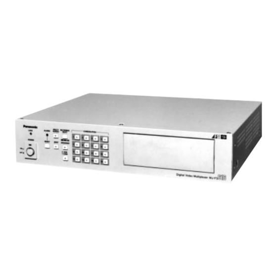
Panasonic WJ-FS616 Service Manual
Video multiplexer
Hide thumbs
Also See for WJ-FS616:
- Operating instructions manual (62 pages) ,
- Operating instruction (60 pages)
Table of Contents
Advertisement
Quick Links
SPECIFICATIONS
Power Source :
Power Consumption :
Camera Input (1-16) :
Camera Output (1-16) :
Spot Output:
Multiscreen Output :
Recording Output :
Playback Input :
Alarm/Remote Control :
VTR Control (RS-232C) :
Ambient Operating Temperature :
Ambient Operating Humidity :
Dimensions :
Weight :
Dimensions and weight are approximate.
Specifications are subject to change without notice.
220 - 240 V AC 50 Hz
50 W
1.0 V[p-p] /75 Ω composite video signal
0.5 V[p-p] /75 Ω data signal and 2.5 V[p-p] /75 Ω vertical timing
pulse multiplexed.
1.0 V[p-p] /75 Ω composite video signal
1.0 V[p-p] /75 Ω composite video signal
1.0 V[p-p] /75 Ω composite video signal
Y Signal; 0.7 V[p-p], C Signal; 0.3 V[p-p] /75Ω S-video signal
1.0 V[p-p] /75 Ω composite video signal
Y Signal; 0.7 V[p-p], C Signal; 0.3 V[p-p] /75Ω S-video signal
1.0 V[p-p] /75 Ω composite video signal
Y Signal; 0.7 V[p-p], C Signal; 0.3 V[p-p] /75Ω S-video signal
37-pin D-sub Connector
25-pin D-sub Connector
−10 °C - +50 °C (14 °F - 122 °F)
Less than 90 %
420 (W) X 88 (H) X 350 (D) mm [16-9/16" (W) X 3-7/16" (H) X 13-3/4" (D)]
6.5 kg (14.3 lbs.)
C 1 9 9 8 M a t s u s h i t a C o m m u n i c a t i o n I n d u s t r i a l C o . , L t d .
A l l r i g h t s r e s e r v e d . U n a u t h o r i z e d c o p y i n g a n d
d i s t r i b u t i o n i s a v i o l a t i o n o f l a w .
ORDER NO. AVS9801086C8
Video Multiplexer
WJ-FS616
Advertisement
Table of Contents

Related Manuals for Panasonic WJ-FS616


Summary of Contents for Panasonic WJ-FS616
- Page 1 ORDER NO. AVS9801086C8 Video Multiplexer WJ-FS616 SPECIFICATIONS Power Source : 220 - 240 V AC 50 Hz Power Consumption : 50 W 1.0 V[p-p] /75 Ω composite video signal Camera Input (1-16) : 0.5 V[p-p] /75 Ω data signal and 2.5 V[p-p] /75 Ω vertical timing pulse multiplexed.
- Page 2 WARNING This service information is designed for experienced repair technicians only and is not designed for use by the general public. It does not contain warnings or cautions to advise non-technical individuals of potential dangers in attempting to service a product. Products powered by electricity should be serviced or repaired only by experienced professional technicians.
-
Page 3: Table Of Contents
Modular Board/Output Board/Communication Board/Alarm Board/Data Multiplex Board ........36 Main Board ................................37 Front Board ................................51 Pocket Board ................................51 Switch Board / Switch Sub Board ..........................52 Power Board ................................53 Exploded View WJ-FS616 ................................. 54 WV-PB6164E................................55 Replacement Parts List ............................. 56... -
Page 4: Major Operating Controls And Their Functions
MAJOR OPERATING CONTROLS AND THEIR FUNCTIONS <Front View> CAMERA/PRESET POSITION MULTI MULTISCREEN PUSH OPEN ALARM SCREEN SELECT LOCK POWER RESET SPOT SEQUENCE CURSOR / CAMERA CONTOROL FUNCTION I R I S SET UP/ESC LOCK CLOSE OPEN VTR CONTROL LEFT HOME/SET RIGHT PRE-POSI FOCUS... - Page 5 7. Multiscreen Selection Button (MULTISCREEN The LED (Green) in the button lights up to indicate that SELECT) the still mode is selected. During the setup, this button is used to select the This button is used to select the multiscreen pattern to desired parameter in the setup menu.
- Page 6 33. VTR Control Buttons These buttons are used for remote control of the VTR that is connected to the Video Multiplexer. The buttons function as shown below. : Rewind : Pause : Fast Forward : Reverse Play : Stop : Play : Decreases recording duration : Increases recording duration : Record...
- Page 7 53. Remote Output Connector (VTR CONTROL, 55. Power Cord REMOTE OUT) 56. Signal Ground Terminal (SIGNAL GND) The VTR control signal for the time lapse VTR is provid- ed via this connector. 57. Termination Switch (TERM., OFF / ON) You can select on the setup menu whether to have the This switch is used to enable termination of the video VTR control signal supplied from this connector or the multiplexer’s data port.
- Page 8 5. Pull out the two knobs from the bracket shown below. 7. Insert the board and confirm that the position is correct. Then remove the bracket. Then push it in straight. 8. After installing the boards, secure them by tightening the screws and knobs shown above.
- Page 9 Dip Switch Setting WJ-FS616 Video Multiplexer Alarm Output Setting Mounting in the Rack 1. Disassemble the video multiplexer as described for 1. Remove the four rubber feet by removing the four installing the Data Multiplex Boards on page 4. screws on the bottom of the video multiplexer.
- Page 10 SYSTEM CONNECTIONS Shown below is an example of a basic system connection. Alarm Video Alarm Sensor Data RS-485 Video Multiplexer WJ-FS616 MULTI MULTISCREEN CAMERA/PRESET POSITION PUSH OPEN ALARM SCREEN SELECT LOCK POWER RESET SPOT SEQUENCE RS-232C/Wired Time Lapse VTR Spot Monitor...
- Page 11 RS-485 “2-wire twist- ed pair shielded cable” is used. camera site and the WJ-FS616 Video Multiplexer is Low grade cable will result in unstable operation of less than 1 200 m (4 000 ft) when using RG-6/U (5C the system.
- Page 12 System Controller, is located on the rear of Switch are located on the rear of the System Controller. the System Controller. When combined with the WJ-FS616 Video Multiplexer, When combined with the WJ-FS616 Video Multiplexer, always keep these switches in the positions shown always keep these switches in the positions shown below.
- Page 13 Connection with the Time Lapse VTR Connect the Time Lapse VTR as shown in the example below. Video Multiplexer WJ-FS616 CAMERA REC OUT PLAY IN SW IN VIDEO S – VIDEO VIDEO S – VIDEO ALARM/REMOTE Time Lapse VTR VIDEO IN...
- Page 14 Connection with External Remote Control Switches Connect the switches (dry contact or open collector input) to the Alarm/Remote (ALARM/REMOTE) Control Connector on the rear of the Video Multiplexer as shown in the example below. Pin No. Designation Pin No. Designation Function Still Picture Electronic Zoom...
-
Page 15: Circuit Description Ic Description
CIRCUIT DESCRIPTION IC Description 1. Switch Board 1.1. IC102 on the Switch Board is using the Single Chip 8-Bit Microprocessor IC YWM380670NET. Description of this IC is as follows: P87 65 40 P20/DB0 39 P21/DB1 P86 66 P85 67 38 P22/DB2 37 P23/DB3 P84 68 36 P24/DB4... - Page 16 1.2. IC69 on the Switch Board is using the On Screen Name Description Display IC YWM35060058. 37 P23/DB3 Description of this IC is as follows: 38 P22/DB2 Data Bus terminals. (8-Bit) 39 P21/DB1 32 CS 31 SCK 40 P20/DB0 30 TESTA 29 P5 41 P15/AD15 28 P4...
- Page 17 1.3. IC86 on the Switch Board is using the 16 X 8 Cross Point Switch IC CD22M3494MQ. Description of this IC is as follows: Name Description 23 Y4 I/O Analog or Digital signal input/output terminal (Column Data Y0 - Y7). 24 AX1 I X Address signal input terminal.
- Page 18 1.4. IC99 on the Switch Board is using the 32,765-Word x 8-Bit High Speed CMOS Static RAM IC YWK58257BM70. Description of this IC is as follows: 28 Vcc 27 WE 26 A13 14 GND 25 A8 28 Vcc 24 A9 23 A11 22 OE (TOP VIEW)
- Page 19 1.5. IC145-IC150 on the Switch Board are using the 16M-Bit Dynamic RAM IC HM14265DJ68. Description of this IC is as follows: Pin Name I/O Description 42 GND I Address signal input terminals. (10-Bit) I/O1 41 I/O16 – Power supply terminal. I/O2 40 I/O15 –...
- Page 20 2. MAIN Board 2.1. IC35 on the Main Board is using the CMOS Gate Array Logic IC YWD65804G089. Description of this IC is as follows: GND 121 80 GND GND 122 79 GND DFULZA 123 78 CLKO 77 CLKI ORUNA 124 BFMPZA 125 76 CLKSTP RXTXZA 126...
- Page 21 Name Description Name Description 33 DGP3_6 O 6CH DGP3 signal output terminal. 77 CLKI I Clock Pulse input terminal. 34 SYNC5 I 5CH Sync signal input terminal. 78 CLKO O Clock Pulse output terminal. 35 DIN5 I 5CH Data input terminal. 79 GND –...
- Page 22 2.2. IC60 on the Main Board is using the Octal 3-State Name Description Inverted Bus Transceivers IC MC74AC640DT. 122 GND – Ground terminal. Description of this IC is as follows: 123 DFULZA O DFULZA signal output terminal. 124 ORUNA O ORUNA signal output terminal. 20 Vcc 125 BFMPZA O BFMZA signal output terminal.
-
Page 23: Adjustment Procedure
2. Disassembling Procedure for the the Vectorscope and Waveform Monitor to the Recording Adjustment Output Connector on the Rear Panel of the WJ-FS616. Terminate the input terminal of the Underscanned Colour Referring to Fig. 2-1, remove five screws that secure the Video Monitor with 75 Ω. - Page 24 Switch Board (set the ACC to Off mode). 4. Adjustment Procedure Refer to the Location of the Test Points and <Start up the WJ-FS616 by the Test Program> Adjusting Controls on the page 28. Turn the Power Switch off.
- Page 25 YF400060CHDT 6 pF (Smaller) + 2.0 V Adjust: VR37 (FSC) Switch Board YF400070CHDT 7 pF YW400080CHJT 8 pF (Typical) Disconnect all input signals from the WJ-FS616. YW400090CHDT 9 pF Connect the Frequency Counter to TP50. YF400100CHJT 10 pF (Larger) Smaller 8 pF Larger Adjust VR37 to obtain 13.500000 MHz ±...
- Page 26 SELF CHECK Video Output Signal TP73 H PHASE(R-2) 00-0F Table 4-2 Connect the Digital Voltmeter to TP28. 8H before the end of Video signal Adjust L116 to obtain 2.0 ± 0.3 V DC. Fig 4-4 Change the connection of the Digital Voltmeter to TP30. Adjust L117 to obtain 2.0 ±...
- Page 27 Execute Program Number 042 Press the Camera Adjust VR35 so that the Burst signal level becomes 300 ± Selection Button/Preset Position Button 4, 2 and 16 14 mV as shown in Fig. 4-6. sequentially, the Menu as shown in Table 4-4 will be dis- Confirm that the Sync signal level becomes 300 ±...
- Page 28 Execute Program Number 033 Press the Camera Change the Ramp signal to the Colour Bar signal. Selection Button/Preset Position Button 3, 3 and 16 Execute Program Number 033 Press the Camera sequentially, the Menu as shown in Table 4-6 will be dis- Selection Button/Preset Position Button 3, 3 and 16 played.
- Page 29 SELF CHECK dø Yellow Cyan 100% 10° 220 ± 7% 155 ± 10% 220 ± 7% Gain 0° 10° 103 ± 5° 167 ± 8° 283 ± 7° Phase Y PED(P –YC) 00-3F Fig 4-10 Table 4-10 Press the Home/Set Button twice. Adjust VR34 so that the Chroma Gain becomes maximum Adjust rest of R-Y and B-Y Gains by executing Program as shown in Fig.
- Page 30 SELF CHECK R–Y GAIN(P –YC) 00-03 Table 4-13 Adjust Direction Arrow Buttons LEFT and/or RIGHT so that the Chroma Vectors position their respective boxes as shown in Fig. 4-12. dø Yellow Cyan 100% 10° 220 ± 7% 155 ± 10% 220 ±...
-
Page 31: Location Of Test Points And Adjusting Controls
LOCATION OF TEST POINTS AND ADJUSTING CONTROLS MAIN BOARD (COMPONENT SIDE) SWITCH BOARD (COMPONENT SIDE) VR23 VR33 (VBS Y GAIN) (Y/C C GAIN) VR22 (Y/C Y GAIN) VR18 (BORDER-1) VR34 (C PHASE) VR35 CN201 CN301 CN401 CN501 CN601 CN701 CN801 CN901 (BURST-2) CN251... -
Page 32: Appearance Of Ics, Transistors And Diodes
APPEARANCE OF IC, TRANSISTOR AND DIODE YWNOKZ YWMVT85038 MC68307PQFP MN73093LBX YWM380670NET MN65752H CD22M3494MQ YWM66220FP HN27C409G YWRF5C81 YWF400BA90PT HM14265DJ68 YWTE7752 YWUPC5022094 1 44 HM628128BFP7 YWK58257BM70 MB90077PF104 YWMSM62X42BR MC74HC138ADT MC74HC4051DT MC74HC04ADT MC74HC32ADT AN1393S YWNJM2267M YWFA5304P YWTC7S00FUL YWM35060058 YWMCHC245AE MC74HC138AF MC74HC4051F YWMC74HC04AF MC74HC74ADT YWBR93LC66RF NJM3414M YWTC7SU04FUR... -
Page 33: Chip Components
CHIP COMPONENTS 2. Chip Diode 4. Chip Capacitor 5-1. Removal (Transistor, Diode, Resistor and 1. Chip Transistor Capacitor) The diode number is indicated on the top surface of the chip The capacitive value of replacement chip capacitors is The transistor number is indicated on the top surface of the 1. -
Page 34: Wiring Diagram
WIRING DIAGRAM CN101 CN102 CN202 CN21 CN103 CN101 CN102 CN51 CN104 VIN+ VIN- DRIVE OUT VOUT AMGND CN203 SYERASE SYNC OUT ERASE DATA OUT CP IN CN21 CN100 MAIN BOARD CABLE M AGND CABLE L AGND DATA IN AGND +5VA TVBS CN100 CN33... -
Page 35: Main Board
BLOCK DIAGRAM OF MAIN BOARD MAIN BOARD DATA MULTIPLEX BOARD Q202(b) Q202(a) CAMERA 1 CN101 Q4(a) BUFFER IC22 CAM1 BUFFER IC37 CAMERA 1 RECEIVER/DRIVER IC13 MICROPROCESSOR CAM2 Q4(b) CN91 Q201 CAM3 CN43 BUFFER RESET RESET CAM4 RX(B) CN202 CN1 +5VA CAM5 RX(A) RSTIN... - Page 36 BLOCK DIAGRAM OF SWITCH BOARD (1/3) SWITCH BOARD (1/3) IC78 6dB VIDEO AMP TO (2/3) SRESET CAM1 IC102 IC101 MICROPROCESSOR CAM2 RESET CN101 EEPROM Q164 SRESET IC86 CAM1 BUFFER CAMSW SPOT CAM2 16x8 CROSS IC79 IDON CAM3 POINT SWITCH 6dB VIDEO AMP IDEQ CAM4 To/From...
- Page 37 BLOCK DIAGRAM OF SWITCH BOARD (2/3) SWITCH BOARD (2/3) IC140 IC145 IC146 IC147 VIDEO SIGNAL PROCESSOR GATE ARRY LOGIC D-RAM D-RAM D-RAM IC1 COMB FILTER L1,L2 124-131 16-20 16-20 16-20 33-40 CIA0A-CIA7A 122-129 57-64 DOA0-DOA7 201-208 C1-C3 D0-D7 CIA0-CIA7 DOA0-DOA7 A YCIN0-YCIN7 23-28 23-28...
-
Page 38: Switch Board / Switch Sub Board
BLOCK DIAGRAM OF SWITCH BOARD (3/3) SWITCH BOARD (3/3) IC35-38 SELECTOR IC39 IC142 IC148 IC149 IC150 IC34 FSSEL5 VIDEO SIGNAL PROCESSOR GATE ARRY LOGIC D-RAM D-RAM D-RAM HIGH SPEED CC0-CC7 PWRN PWRN A/D CONVERTER 122-129 124-131 16-20 16-20 16-20 CIA0E-CIA7E 57-64 DOE0-DOE7 201-208... -
Page 39: Exploded View
Internal Toothed Lock Washers PCB9 XUC2VW Retaining Rings "Type E" XSB2+6FX Binding Head Screw Serial No. Label XSB4+8FN Binding Head Screw XSB3+8FN Binding Head Screws XTB3+5FFX Binding Head Tapping Screw PCB10 PCB8 PCB1 PACKAGING P101 WJ-FS616 PCB2 – 54 –... -
Page 40: Wv-Pb6164E
EXPLODED VIEW OF WV-PB6164E Serial No. Label PCB1 PACKAGING WV-PB6164E Serial No. Label... - Page 41 Printed in Japan N N 5, 7, 23 C-661...