Panasonic WJ-FS216 Service Manual
Video multiplexer
Hide thumbs
Also See for WJ-FS216:
- Operating instructions manual (28 pages) ,
- Operating instructions manual (28 pages) ,
- Operating instructions manual (30 pages)
Advertisement
Quick Links
SPECIFICATIONS
Power Source :
Power Consumption :
Camera Input :
Playback Input :
Monitor Output :
Recording Output :
Camera Switching Input :
Alarm Input :
Alarm Output :
Alarm Recover Input :
Operating Temperature :
Operating Humidity :
Dimensions :
Weight :
Dimensions and weight are approximate.
Specifications are subject to change without notice.
STANDARD ACCESSORIES
Rack Mounting Angle .......................................... 2 pcs.
Screws (M3 x 10)................................................. 8 pcs.
Switch Protector .................................................. 1 pc.
220 - 240 V AC 50 Hz
12 W
16 (BNC) 2:1 interlaced VBS 1.0V[p-p]/75 Ω automatic termination/looping through
1 (BNC) VBS 1.0V[p-p]/75 Ω
1 (BNC) VBS 1.0V[p-p]/75 Ω
1 (BNC) VBS 1.0V[p-p]/75 Ω
1 RCA pin jack
16
1 Open-collector 24V DC 100 mA max.
1
−10°C - +50°C (14°F - 122°F)
Less than 90%
420 (W) x 44 (H) x 350 (D) [16-9"(W) x 3-7/16(H) x 13-3/4"(D)]
4 kg (8.8 lbs)
C 1 9 9 7 M a t s u s h i t a C o m m u n i c a t i o n I n d u s t r i a l C o . , L t d .
A l l r i g h t s r e s e r v e d . U n a u t h o r i z e d c o p y i n g a n d
d i s t r i b u t i o n i s a v i o l a t i o n o f l a w .
ORDER NO. AVS9712082C8
Video Multiplexer
WJ-FS216
Advertisement

Related Manuals for Panasonic WJ-FS216


Summary of Contents for Panasonic WJ-FS216
- Page 1 ORDER NO. AVS9712082C8 Video Multiplexer WJ-FS216 SPECIFICATIONS Power Source : 220 - 240 V AC 50 Hz Power Consumption : 12 W 16 (BNC) 2:1 interlaced VBS 1.0V[p-p]/75 Ω automatic termination/looping through Camera Input : 1 (BNC) VBS 1.0V[p-p]/75 Ω...
-
Page 2: Table Of Contents
WARNING This service information is designed for experienced repair technicians only and is not designed for use by the general public. It does not contain warnings or cautions to advise non-technical individuals of potential dangers in attempting to service a product. Products powered by electricity should be serviced or repaired only by experienced professional technicians. -
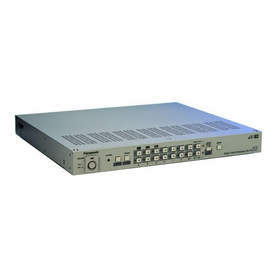
Page 3: Major Operating Controls And Their Functions
MAJOR OPERATING CONTROLS AND THEIR FUNCTIONS Panasonic CAMERA/VTR MODE ALARM ZOOM MENU POWER SELECT SEQENCE MULTI SCREEN CAMERA ALARMRESET QUAD SHIFT SELECT Digital Video MultiplexerWJ-FS STILL ON CAMERA CAMERA SW IN PLAY IN REC OUT MONITOR OUT CAMERA SIGNAL ALARM/REMOTE 1. - Page 4 Button No.15 (SET) 5. Camera Selection Button (1...16, This button is used as the SET button in setting proce- CAMERA/VTR, D, C, A, B, –, +, SET, STILL ON) dures. When the MODE SELECT/CAMERA SELECT switch is in CAMERA SELECT position, these buttons can be Button No.16 (STILL ON) used to select the desired camera.
- Page 5 RACK MOUNTING 13. Recording Output Connector (REC OUT) This connector supplies the recording signal for the time To install the WJ-FS216 Video Multiplexer in an EIA 19-inch lapse VTR. rack, use the rack mounting brackets (provided) and eight Caution: screws (provided, M3x10).
- Page 6 CONNECTION Refer to the operating instructions of each system component for connection and opera- tion. Cameras Cameras Video Monitor Camera Drive Unit VIDEO INPUT VIDEO OUTPUT CAMERA CAMERA SW IN CAMERA PLAY IN REC OUT MONITOR OUT SIGNAL ALARM/REMOTE Cameras Time Lapse VTR VIDEO OUTPUT...
- Page 7 Power capacity of alarm output connector more than 100 • Connection with the Alarm Sensor You can connect an alarm sensor to record the pictures • Connect the buzzer through a relay circuit to pin 24 of channels that receive alarm input signal. of the alarm output connector.
- Page 8 Connection with the Time Lapse VTR Connect the time lapse VTR as shown in the example below. Video Multiplexer WJ-FS216 CAMERA SW IN PLAY IN REC OUT ALARM/REMOTE 24 22 Time Lapse VTR VIDEO IN VIDEO OUT S-VIDEO AUDIO CAMERA...
- Page 9 • Remote Control You can control the SEQUENCE, MULTISCREEN/QUAD SHIFT, and the camera selection buttons from a remote con- troller. These functions are activated by contact with the ground terminal (open collector output or normally open con- tact). • Connect the ALARM/REMOTE connector (pin 23) to the ground terminal as shown below. Switches 1 - 16 select the cameras (they do not control the alarm input).
-
Page 10: Circuit Description Ic Description
CIRCUIT DESCRIPTION IC Description 1. Main Board 1.1. IC623 on the Main Board is using the Digital Signal Processor IC YWD65621G045. Description of this IC is as follows: Name Description 26 GND – Ground terminal. 27 V – Power supply terminal. VPA 52 32 YA3 28 YA7... - Page 11 1.2. IC403, IC404 and IC616 on the Main Board are using the Dynamic RAM IC HM14265DJ68. Description of this IC is as follows: Name Description 40 Vss 17 A1 39 I/O15 I/O0 18 A2 I Address signal input terminals. (9-Bit) 38 I/O14 I/O1 19 A3...
- Page 12 1.3. IC615 on the Main Board is using the Gate Array Logic IC YWNOKZ. Description of this IC is as follows: A PLLV 120 GND A PLLGND 182 119 CAS A CPOUT 183 118 WE A REFCLK 184 117 OE A W4FSC 185 116 MC 0 A TEST 186...
- Page 13 Name Description Name Description 17 D WFLD I D Wide Field Pulse input terminal. 62 RSYDET O RSY Detect signal output terminal. 18 D W27M I D Clock Pulse input terminal. 63 REXHIL I REXHIL signal input terminal. 19 D QYRB0 64 GND –...
- Page 14 Name Description Name Description 108 GND – Ground terminal. 153 MB1 MB signal output terminals. 109 MC7 154 MB0 110 MC6 155 B W27MO O B W27M Clock Pulse output terminal. 111 MC5 156 B WFLDO O B Wide Field Pulse output terminal. 112 MC4 157 MA15 MC Data input/output terminals.
- Page 15 1.4. IC111 on the Main Board is using the 4K (256-Word Name Description x 16-Bit) Serial 3-Line EEPROM IC YWBR93LC 199 A WVCOO O A WVCO signal output terminal. 66RF. 200 K TEST I Test signal input terminal. Description of this IC is as follows: 201 A YCIN0 202 A YCIN1 CS 1...
- Page 16 1.5. IC122 on the Main Board is using the 8-Bit Single Chip Microprocessor IC YW38004E8121. Description of this IC is as follows: Name Description 27 P25 28 P24 RD 49 32 P20 29 P23 WR 50 31 P21 Data input/output terminals. (8-Bit) P35 51 30 P22 30 P22...
- Page 17 1.6. IC101 on the Main Board is using the Video Signal Processor IC YWMVT85038. Description of this IC is as follows: 80 V CIA7 122 79 COA0 CIA6 123 78 COA1 CIA5 124 77 COA2 76 COA3 CIA4 125 CIA3 126 75 COA4 74 COA5 CIA2 127...
- Page 18 Name Description Name Description 29 V – Power supply terminal. 75 COA4 30 GND – Ground terminal. 76 COA3 31 DOB7 77 COA2 O COA Data output terminals. (8-Bit) 32 DOB6 78 COA1 33 DOB5 79 COA0 80 V – Power supply terminal. 34 DOB4 DOB Data output terminals.
- Page 19 Name Description 121 V – Power supply terminal. 122 CIA7 123 CIA6 124 CIA5 125 CIA4 CIA Data input terminals. (8-Bit) 126 CIA3 127 CIA2 128 CIA1 129 CIA0 130 CPSIGB I B COSIG signal input terminal. 131 GND – Ground terminal. 132 V –...
-
Page 20: Adjustment Procedure
Connect the Underscanned Colour Video Monitor through 1. Test Equipments Required the Vectorscope and Waveform Monitor to the Recording Output Connector on the Rear Panel of the WJ-FS216. The following Test Equipments are required for adjust- Terminate the input terminal of the Underscanned Colour ment of the Video Multiplexer WJ-FS216. -
Page 21: Main Board/D-Sub Board/Rear Board
Confirm that the Sync signal level becomes 300 ± 30 Turn the Power Switch off. mVp-p as shown in Fig. 4-3. Disconnect all input signals from the WJ-FS216. Connect the Frequency Counter to TP409 and TP113 (GND). Turn the Power Switch on while pressing the Cursor ( ) 700 ±... - Page 22 (4). Decoder Section Adjustment Chroma Pedestal level should be less than Test Point: Recording Output Connector Rear Panel Burst 35 mV. Adjust: VR102 (Y LEVEL) Main Board VR106 (C GAIN) Main Board VR105 (C PHASE) Main Board Cursor (+) or (–) Fig.
- Page 23 CHIP COMPONENTS 2. Chip Diode 1. Chip Transistor The diode number is indicated on the top surface of the chip The transistor number is indicated on the top surface of the diode using two alphabet letters. chip transistor using two alphabet letters or one numerical number and two alphabet letters.
- Page 24 4. Chip Capacitor 5-1. Removal (Transistor, Diode, Resistor and Capacitor) The capacitive value of replacement chip capacitors is 1. Add the solder to both ends of the chip (three leads for indicated on the bottom surface. Original parts have no chip transistor).
- Page 30 Printed in Japan C-660 N 5, 7, 23...