Table of Contents
Advertisement
Quick Links
Service Guide
Publication Number 33250-90011 (order as 33250-90100 manual set)
Edition 2, March 2003
© Copyright Agilent Technologies, Inc. 2000, 2003
For Safety information, Warranties, and Regulatory information,
see the pages following the Index.
Agilent 33250A
80 MHz Function /
Arbitrary Waveform Generator
Advertisement
Table of Contents

Related Manuals for Agilent Technologies 33250A


Summary of Contents for Agilent Technologies 33250A
- Page 1 Service Guide Publication Number 33250-90011 (order as 33250-90100 manual set) Edition 2, March 2003 © Copyright Agilent Technologies, Inc. 2000, 2003 For Safety information, Warranties, and Regulatory information, see the pages following the Index. Agilent 33250A 80 MHz Function /...
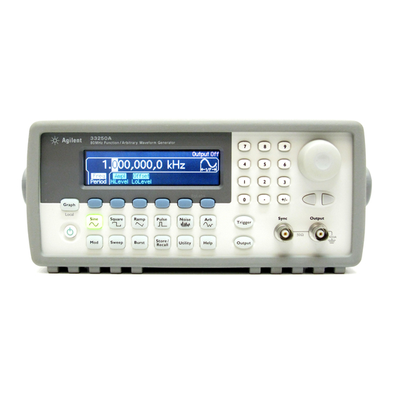
- Page 2 Agilent 33250A at a Glance The Agilent Technologies 33250A is a high-performance 80 MHz synthesized function generator with built-in arbitrary waveform and pulse capabilities. Its combination of bench-top and system features makes this function generator a versatile solution for your testing requirements now and in the future.
- Page 3 The Front Panel at a Glance 1 Graph Mode/Local Key 7 Utility Menu 2 Menu Operation Softkeys 8 Instrument Help Topic Menu 3 Waveform Selection Keys 9 Output Enable/Disable Key 4 Knob 10 Manual Trigger Key (used for 5 Modulation/Sweep/Burst Menus Sweep and Burst only) 6 State Storage Menu 11 Cursor Keys...
- Page 4 The Front-Panel Display at a Glance Menu Mode Mode Trigger Output Information Information Units Status Display Numeric Icon Readout Softkey Labels Graph Mode To enter the Graph Mode, press the key. Parameter Parameter Name Value Signal Ground The softkey colors correspond to the waveform parameters.
- Page 5 Front-Panel Number Entry You can enter numbers from the front-panel using one of two methods. Use the knob and arrow keys to modify the displayed number. Use the numeric keypad and menu softkeys to select the units.
- Page 6 The Rear Panel at a Glance 1 External 10 MHz Reference Input Terminal 5 Input: External Trig/FSK/Burst Gate 2 Internal 10 MHz Reference Output Terminal Output: Trigger Output 3 RS-232 Interface Connector 6 GPIB Interface Connector 4 External Modulation Input Terminal 7 Chassis Ground Use the menu to:...
- Page 7 Schematics Chapter 9 contains the function generator’s schematics and component locator drawings. If you have questions relating to the operation of the Agilent 33250A, call 1-800-452-4844 in the United States, or contact your nearest Agilent Technologies Office.
-
Page 9: Table Of Contents
To Unsecure and Secure for Calibration 41 To Store the Instrument State 44 To Configure the Remote Interface 45 Chapter 4 Calibration Procedures Agilent Technologies Calibration Services 49 Calibration Interval 50 Adjustment is Recommended 50 Time Required for Calibration 51... - Page 10 Contents Chapter 4 Calibration Procedures (continued) Calibration Security 68 Calibration Message 70 Calibration Count 70 General Calibration/Adjustment Procedure 71 Aborting a Calibration in Progress 72 Sequence of Adjustments 72 Self-Test 73 Frequency (Internal Timebase) Adjustment 74 Internal ADC Adjustment 75 Output Impedance Adjustment 76 AC Amplitude (high-impedance) Adjustment 78 Low Frequency Flatness Adjustment 80...
- Page 11 Surface Mount Repair 133 Troubleshooting Hints 134 Self-Test Procedures 136 Disassembly 140 Chapter 7 Replaceable Parts 33250-66511 Main PC Assembly (A1) 153 33205-66502 Front-Panel PC Assembly (A2) 176 33250A Chassis Assembly 177 33250A Front-Panel Assembly 178 Manufacturer’s List 179 Chapter 8 Backdating 181...
- Page 12 Contents Chapter 9 Schematics A1 Earth Referenced Communications Schematic 185 A1 Main Processor Schematic 186 A1 Main Gate Array Schematic 187 A1 Display Controller Schematic 188 A1 DSP Schematic 189 A1 Modulation Schematic 190 A1 System DAC Schematic 191 A1 Timebase Schematic 192 A1 Phase-Locked Loops Schematic 193 A1 Trigger Schematic 194 A1 Clock Divider and Control Schematic 195...
-
Page 13: Chapter 1 Specifications
Specifications... - Page 14 Chapter 1 Specifications Agilent 33250A Function / Arbitrary Waveform Generator WAVEFORMS SIGNAL CHARACTERISTICS Standard Waveforms: Sine, Square, Ramp, Square Wave Pulse, Noise, Sin(x)/x, Rise / Fall Time: < 8 ns Exponential Rise, Overshoot: < 5% Exponential Fall, Asymmetry: 1% of period + 1 ns...
- Page 15 Chapter 1 Specifications Agilent 33250A Function / Arbitrary Waveform Generator OUTPUT CHARACTERISTICS BURST Amplitude (into 50Ω): 10 mVpp to 10 Vpp Waveforms: Sine, Square, Ramp, Pulse, Noise, Arb Accuracy (at 1 kHz, >10 mVpp, Autorange On): Frequency: 1 µHz to 80 MHz ±...
- Page 16 Chapter 1 Specifications Agilent 33250A Function / Arbitrary Waveform Generator SYSTEM CHARACTERISTICS CLOCK REFERENCE Configuration TImes (typical) Phase Offset Range: -360° to +360° Function Change Resolution: 0.001° Standard: 102 ms Pulse: 660 ms External Reference Input Built-In Arb: 240 ms Lock Range: 10 MHz ±...
- Page 17 Chapter 1 Specifications Agilent 33250A Function / Arbitrary Waveform Generator GENERAL SPECIFICATIONS Power Supply: 100-240 V (±10%) Safety Designed to: EN61010-1, CSA1010.1, for 50-60 Hz operation, UL-3111-1 100-127 V (±10%) for 50-400 Hz operation. EMC Tested to: IEC-61326-1 IEC 60664 CAT II...
- Page 18 Chapter 1 Specifications Agilent 33250A Function / Arbitrary Waveform Generator PRODUCT DIMENSIONS 103.6 mm 254.4 mm 374.0 mm 88.5 mm 216.6 mm 348.3 mm All dimensions are shown in millimeters.
-
Page 19: Chapter 2 Quick Start
Quick Start... - Page 20 Quick Start One of the first things you will want to do with your function generator is to become acquainted with the front panel. We have written the exercises in this chapter to prepare the instrument for use and help you get familiar with some of its front-panel operations.
-
Page 21: To Prepare The Function Generator For Use
Chapter 2 Quick Start To Prepare the Function Generator for Use To Prepare the Function Generator for Use 1 Check the list of supplied items. Verify that you have received the following items with your instrument. If anything is missing, please contact your nearest Agilent Sales Office. ❑... -
Page 22: To Adjust The Carrying Handle
Chapter 2 Quick Start To Adjust the Carrying Handle To Adjust the Carrying Handle To adjust the position, grasp the handle by the sides and pull outward. Then, rotate the handle to the desired position. Bench-top viewing positions Carrying position... -
Page 23: To Set The Output Frequency
Chapter 2 Quick Start To Set the Output Frequency To Set the Output Frequency At power-on, the function generator outputs a sine wave at 1 kHz with an amplitude of 100 mV peak-to-peak (into a 50Ω termination). The following steps show you how to change the frequency to 1.2 MHz. 1 Press the “Freq”... -
Page 24: To Set The Output Amplitude
Chapter 2 Quick Start To Set the Output Amplitude To Set the Output Amplitude At power-on, the function generator outputs a sine wave with an amplitude of 100 mV peak-to-peak (into a 50Ω termination). The following steps show you how to change the amplitude to 50 mVrms. 1 Press the “Ampl”... - Page 25 Chapter 2 Quick Start To Set the Output Amplitude You can easily convert the displayed amplitude from one unit to another. For example, the following steps show you how to convert the amplitude from Vrms to Vpp. 4 Enter the numeric entry mode. Press the key to enter the numeric entry mode.
-
Page 26: To Set A Dc Offset Voltage
Chapter 2 Quick Start To Set a DC Offset Voltage To Set a DC Offset Voltage At power-on, the function generator outputs a sine wave with a dc offset of 0 volts (into a 50Ω termination). The following steps show you how to change the offset to –1.5 mVdc. -
Page 27: To Set The Duty Cycle
Chapter 2 Quick Start To Set the Duty Cycle To Set the Duty Cycle Applies only to square waves. At power-on, the duty cycle for square waves if 50%. You can adjust the duty cycle from 20% to 80% for output frequencies up to 25 MHz. -
Page 28: To Configure A Pulse Waveform
Chapter 2 Quick Start To Configure a Pulse Waveform To Configure a Pulse Waveform You can configure the function generator to output a pulse waveform with variable pulse width and edge time. The following steps show you how to configure a 500 ms pulse waveform with a pulse width of 10 ms and edge times of 50 µs. -
Page 29: To View A Waveform Graph
Chapter 2 Quick Start To View a Waveform Graph To View a Waveform Graph In the Graph Mode, you can view a graphical representation of the current waveform parameters. Each softkey parameter is shown in a different color corresponding to the lines above the softkeys at the bottom of the display. -
Page 30: To Output A Stored Arbitrary Waveform
Chapter 2 Quick Start To Output a Stored Arbitrary Waveform To Output a Stored Arbitrary Waveform There are five built-in arbitrary waveforms stored in non-volatile memory. The following steps show you how to output the built-in “exponential fall” waveform from the front panel. 1 Select the arbitrary waveform function. -
Page 31: To Use The Built-In Help System
Chapter 2 Quick Start To Use the Built-In Help System To Use the Built-In Help System The built-in help system is designed to provide context-sensitive assistance on any front-panel key or menu softkey. A list of help topics is also available to assist you with several front-panel operations. 1 View the help information for a function key. - Page 32 Chapter 2 Quick Start To Use the Built-In Help System 3 View the list of help topics. Press the key to view the list of available help topics. To scroll through the list, press the ↑ or ↓ softkey or rotate the knob. Select the third topic “Get HELP on any key”...
-
Page 33: To Rack Mount The Function Generator
To Rack Mount the Function Generator To Rack Mount the Function Generator You can mount the Agilent 33250A in a standard 19-inch rack cabinet using one of two optional kits available. Instructions and mounting hardware are included with each rack-mounting kit. Any Agilent System II instrument of the same size can be rack-mounted beside the Agilent 33250A. - Page 34 Chapter 2 Quick Start To Rack Mount the Function Generator To rack mount a single instrument, order adapter kit 5063-9240. To rack mount two instruments side-by-side, order lock-link kit 5061-9694 and flange kit 5063-9212. Be sure to use the support rails in the rack cabinet. In order to prevent overheating, do not block the flow of air into or out of the instrument.
-
Page 35: Chapter 3 Front-Panel Menu Operation
Front-Panel Menu Operation... - Page 36 This chapter does not give a detailed description of every front-panel key or menu operation. It does, however, give you an overview of the front- panel menus and many front-panel operations. See the Agilent 33250A User’s Guide for a complete discussion of the function generator’s capabilities and operation.
-
Page 37: Front-Panel Menu Reference
Chapter 3 Front-Panel Menu Operation Front-Panel Menu Reference Front-Panel Menu Reference This section gives an overview of the front-panel menus. The remainder of this chapter shows examples of using the front-panel menus. Configure the modulation parameters for AM, FM, and FSK. •... - Page 38 Chapter 3 Front-Panel Menu Operation Front-Panel Menu Reference Store and recall instrument states. • Store up to four instrument states in non-volatile memory. • Assign a custom name to each storage location. • Recall stored instrument states. • Restore all instrument settings to their factory default values. •...
-
Page 39: To Reset The Function Generator
“Factory Default Settings” table inside the rear cover of this manual. To Select the Output Termination The Agilent 33250A has a fixed series output impedance of 50 ohms to the front-panel Output connector. If the actual load impedance is different than the value specified, the displayed amplitude and offset levels will be incorrect. -
Page 40: To Read The Calibration Information
Chapter 3 Front-Panel Menu Operation To Read the Calibration Information To Read the Calibration Information You can use the instrument’s calibration memory to read the calibration count and calibration message. Calibration Count You can query the instrument to determine how many calibrations have been performed. -
Page 41: To Unsecure And Secure For Calibration
Chapter 3 Front-Panel Menu Operation To Unsecure and Secure for Calibration To Unsecure and Secure for Calibration This feature allows you to enter a security code to prevent accidental or unauthorized adjustments of the instrument. When you first receive your instrument, it is secured. Before you can adjust the instrument, you must unsecure it by entering the correct security code. - Page 42 Chapter 3 Front-Panel Menu Operation To Unsecure and Secure for Calibration To Unsecure for Calibration 1 Select the Secure Code interface. Press and then select the Test/Cal softkey. 2 Enter the Secure Code. Use the knob to change the displayed character. Use the arrow keys to move to the next character.
- Page 43 Chapter 3 Front-Panel Menu Operation To Unsecure and Secure for Calibration To Secure After Calibration 1 Select the Secure Code interface. Press and then select the Test/Cal softkey. 2 Enter a Secure Code. Enter up to 12 alphanumeric characters. The first character must be a letter.
-
Page 44: To Store The Instrument State
Chapter 3 Front-Panel Menu Operation To Store the Instrument State To Store the Instrument State You can store the instrument state in one of four non-volatile storage locations. A fifth storage location automatically holds the power-down configuration of the instrument. When power is restored, the instrument can automatically return to its state before power-down. -
Page 45: To Configure The Remote Interface
Chapter 3 Front-Panel Menu Operation To Configure the Remote Interface To Configure the Remote Interface The instrument is shipped with both a GPIB (IEEE-488) interface and an RS-232 interface. Only one interface can be enabled at a time. The GPIB interface is selected when the instrument is shipped from the factory. - Page 46 Chapter 3 Front-Panel Menu Operation To Configure the Remote Interface RS-232 Configuration 1 Select the RS-232 interface. Press and then select the RS-232 softkey from the “I/O” menu. 2 Set the baud rate. Press the Baud Rate softkey and select one of the following: 300, 600, 1200, 2400, 4800, 9600, 19200, 38400, 57600 (factory setting), or 115200 baud.
-
Page 47: Chapter 4 Calibration Procedures
Calibration Procedures... - Page 48 This chapter contains procedures for verification of the instrument’s performance and adjustment (calibration). The chapter is divided into the following sections: • Agilent Technologies Calibration Services, on page 49 • Calibration Interval, on page 50 • Adjustment is Recommended, on page 50 •...
-
Page 49: Agilent Technologies Calibration Services
Agilent Technologies Calibration Services When your instrument is due for calibration, contact your local Agilent Technologies Service Center for a low-cost recalibration. The Agilent 33250A is supported on automated calibration systems which allow Agilent to provide this service at competitive prices. -
Page 50: Calibration Interval
Whatever calibration interval you select, Agilent Technologies recommends that complete re-adjustment should always be performed at the calibration interval. This will assure that the Agilent 33250A will remain within specification for the next calibration interval. This criteria for re-adjustment provides the best long-term stability. -
Page 51: Time Required For Calibration
Chapter 4 Calibration Procedures Time Required for Calibration Time Required for Calibration The Agilent 33250A can be automatically calibrated under computer control. With computer control you can perform the complete calibration procedure and performance verification tests in approximately 30 minutes once the instrument is warmed-up (see “Test Considerations”... -
Page 52: Automating Calibration Procedures
The calibration value is sent to the instrument and then the calibration is initiated over the remote interface. The instrument must be unsecured prior to initiating the calibration procedure. For further information on programming the instrument, see chapters 3 and 4 in the Agilent 33250A User’s Guide. -
Page 53: Recommended Test Equipment
Chapter 4 Calibration Procedures Recommended Test Equipment Recommended Test Equipment The test equipment recommended for the performance verification and adjustment procedures is listed below. If the exact instrument is not available, substitute calibration standards of equivalent accuracy. Instrument Requirements Recommended Model Use* Digital Multimeter ac volts, true rms, ac coupled... -
Page 54: Test Considerations
Chapter 4 Calibration Procedures Test Considerations Test Considerations For optimum performance, all procedures should comply with the following recommendations: • Assure that the calibration ambient temperature is stable and between 18 °C and 28 °C. Ideally, the calibration should be performed at 23 °C 1 °C. -
Page 55: Performance Verification Tests
Chapter 4 Calibration Procedures Performance Verification Tests Performance Verification Tests Use the Performance Verification Tests to verify the measurement performance of the instrument. The performance verification tests use the instrument’s specifications listed in the “Specifications” chapter beginning on page 13. You can perform four different levels of performance verification tests: •... - Page 56 Chapter 4 Calibration Procedures Performance Verification Tests Self-Test A brief power-on self-test occurs automatically whenever you turn on the instrument. This limited test assures that the instrument is operational. To perform a complete self-test: 1 Press on the front panel. 2 Select the Self Test softkey from the “Test/Cal”...
- Page 57 Chapter 4 Calibration Procedures Performance Verification Tests Quick Performance Check The quick performance check is a combination of internal self-test and an abbreviated performance test (specified by the letter Q in the performance verification tests). This test provides a simple method to achieve high confidence in the instrument’s ability to functionally operate and meet specifications.
- Page 58 Chapter 4 Calibration Procedures Performance Verification Tests Amplitude and Flatness Verification Procedures Special Note: Measurements made during the AC Amplitude (high- impedance) Verification procedure (see page 61) are used as reference measurements in the flatness verification procedures (beginning on page 62). Additional reference measurements and calculated references are used in the flatness verification procedures.
- Page 59 Chapter 4 Calibration Procedures Performance Verification Tests Amplitude and Flatness Verification Worksheet 1. Enter the following measurements (from procedure on page 61). 1kHz_0dB_reference = __________________________ Vrms 1kHz_10dB_reference = __________________________ Vrms 1kHz_20dB_reference = __________________________ Vrms 2. Calculate the dBm value of the rms voltages. 1kHz_0dB_reference_dBm 10 * log(5.0 * 1kHz_0dB_reference __________________________ dBm...
-
Page 60: Internal Timebase Verification
1 Connect a frequency counter as shown below (the frequency counter Ω input should be terminated at 50 2 Set the instrument to the output described in the table below and measure the output frequency. Be sure the instrument output is enabled. Agilent 33250A Measurement Function Amplitude Frequency... -
Page 61: Ac Amplitude (High-Impedance) Verification
2 Set the instrument to each output described in the table below and measure the output voltage with the DMM. Press to set the output impedance to High-Z. Be sure the output is enabled. Agilent 33250A Measurement Output Setup Function... -
Page 62: Low Frequency Flatness Verification
2 Set the instrument to each output described in the table below and measure the output voltage with the DMM. Press to set the output impedance to High-Z. Be sure the output is enabled. Agilent 33250A Measurement Output Setup Function... -
Page 63: Db Range Flatness Verification
Chapter 4 Calibration Procedures 0 dB Range Flatness Verification 0 dB Range Flatness Verification This procedure checks the high frequency ac amplitude flatness above 100 kHz on the 0 dB attenuator range. 1 Connect the power meter to measure the output amplitude of the instrument as shown below. - Page 64 3 Set the instrument to each output described in the table below and measure the output amplitude with the power meter. Press to set the output impedance to 50Ω. Be sure the output is enabled. Agilent 33250A Measurement Output Setup Function...
-
Page 65: Db Range Flatness Verification
3 Set the instrument to each output described in the table below and measure the output amplitude with the power meter. Press to set the output impedance to 50Ω. Be sure the output is enabled. Agilent 33250A Measurement Output Setup Function... -
Page 66: Db Range Flatness Verification
Chapter 4 Calibration Procedures +20 dB Range Flatness Verification +20 dB Range Flatness Verification This procedure checks the high frequency ac amplitude flatness above 100 kHz on the +20 dB attenuator range. 1 Connect the power meter to measure the output voltage of the instrument as shown below. - Page 67 3 Set the instrument to each output described in the table below and measure the output amplitude with the power meter. Press to set the output impedance to 50Ω. Be sure the output is enabled Agilent 33250A Measurement Output Setup Function...
-
Page 68: Calibration Security
Chapter 4 Calibration Procedures Calibration Security Calibration Security This feature allows you to enter a security code to prevent accidental or unauthorized adjustments of the instrument. When you first receive your instrument, it is secured. Before you can adjust the instrument, you must unsecure it by entering the correct security code. - Page 69 Chapter 4 Calibration Procedures Calibration Security To Unsecure the Instrument Without the Security Code To unsecure the instrument without the correct security code, follow the steps below. See “To Unsecure and Secure for Calibration” on page 41. See “Electrostatic Discharge (ESD) Precautions” on page 133 before beginning this procedure.
-
Page 70: Calibration Message
Chapter 4 Calibration Procedures Calibration Message Calibration Message The instrument allows you to store one message in calibration memory. For example, you can store such information as the date when the last calibration was performed, the date when the next calibration is due, the instrument’s serial number, or even the name and phone number of the person to contact for a new calibration. -
Page 71: General Calibration/Adjustment Procedure
Chapter 4 Calibration Procedures General Calibration/Adjustment Procedure General Calibration/Adjustment Procedure The following procedure is the recommended method to complete an instrument calibration. This procedure is an overview of the steps required for a complete calibration. Additional details for each step in this procedure are given in the appropriate sections of this chapter. -
Page 72: Aborting A Calibration In Progress
Chapter 4 Calibration Procedures Aborting a Calibration in Progress Aborting a Calibration in Progress Sometimes it may be necessary to abort a calibration after the procedure has already been initiated. You can abort a calibration at any time by turning off the power. When performing a calibration from the remote interface, you can abort a calibration by issuing a remote interface device clear message followed by a *RST . -
Page 73: Self-Test
Chapter 4 Calibration Procedures Self-Test Self-Test Self-Test is performed as the first step to ensure the instrument is in working order before beginning any additional adjustments. 1 Press on the front panel. Select Perform Cal on the “Test / Cal” menu. -
Page 74: Frequency (Internal Timebase) Adjustment
Chapter 4 Calibration Procedures Frequency (Internal Timebase) Adjustment Frequency (Internal Timebase) Adjustment The function generator stores a calibration constant that sets the TCXO to output exactly 10 MHz. 1 Set the frequency counter resolution to better than 0.1 ppm and the input termination to 50Ω... -
Page 75: Internal Adc Adjustment
Chapter 4 Calibration Procedures Internal ADC Adjustment Internal ADC Adjustment The function generator stores calibration constants related to the gain and offset of the internal ADC. Setup 6 must always be performed before any other adjustments are attempted. The internal ADC is then used as a source for the calibration constants generated in setup 7. -
Page 76: Output Impedance Adjustment
Chapter 4 Calibration Procedures Output Impedance Adjustment 5 Enter and begin the following setup. Setup Self-calibration. The Main Output is disabled during test. * Constants are stored after completing this setup. 6 There are no specific operational verification tests for setups 6 and 7 since the constants generated affect almost all behavior of the instrument. - Page 77 Chapter 4 Calibration Procedures Output Impedance Adjustment 2 Use the DMM to make a resistance measurement at the front panel Output connector for each setup in the following table. The expected measured value is approximately 50Ω. Setup -30 dB range with distortion filter -20 dB range with distortion filter -10 dB range with distortion filter 0 dB range with distortion filter...
-
Page 78: Ac Amplitude (High-Impedance) Adjustment
Chapter 4 Calibration Procedures AC Amplitude (high-impedance) Adjustment AC Amplitude (high-impedance) Adjustment The function generator stores a calibration constant for each high- impedance attenuator path. The gain coefficient of each path is calculated using two measurements; one with the waveform DAC at the + output and one with waveform DAC at the –... - Page 79 Chapter 4 Calibration Procedures AC Amplitude (high-impedance) Adjustment 2 Use the DMM to measure the dc voltage at the front-panel Output connector for each setup in the following table. Nominal Signal Setup DC level +0.015 V Output of -30 dB range -0.015 V Output of -30 dB range +0.05 V...
-
Page 80: Low Frequency Flatness Adjustment
Chapter 4 Calibration Procedures Low Frequency Flatness Adjustment Low Frequency Flatness Adjustment The Low Frequency Flatness adjustment calculates the flatness response of 3 attenuator paths with the Elliptical filter and 2 attenuator paths with the Linear Phase filter. 1 Set the DMM to measure Vrms. Make the connections shown on page 78. 2 Use the DMM to measure the output voltage for each of the setups in the table below. -
Page 81: Db Range Flatness Adjustments
Chapter 4 Calibration Procedures 0 dB Range Flatness Adjustments 0 dB Range Flatness Adjustments 1 Connect the power meter as shown on page 83. 2 Use the power meter to measure the output amplitude for each of the setups in the table below. Setup 44 establishes the power meter reference for all the remaining Note setups in this table. - Page 82 Chapter 4 Calibration Procedures 0 dB Range Flatness Adjustments Nominal Signal Setup Frequency Amplitude 200 kHz 0.28 Vrms 2 dBm Flatness for 0 dB, Linear Phase 500 kHz 0.28 Vrms 2 dBm Flatness for 0 dB, Linear Phase 1.5 MHz 0.28 Vrms 2 dBm Flatness for 0 dB, Linear Phase...
-
Page 83: Db Range Flatness Adjustments
Chapter 4 Calibration Procedures +10 dB Range Flatness Adjustments +10 dB Range Flatness Adjustments The Linear Phase path is not adjusted. It is approximated using the other Note path’s values. 1 Connect the power meter as shown below. 2 Use the power meter to measure the output amplitude for each of the setups in the table on the next page. - Page 84 Chapter 4 Calibration Procedures +10 dB Range Flatness Adjustments Nominal Signal Setup Frequency Amplitude 100 kHz 0.9 Vrms 12 dBm Power Meter Reference for +10 dB Range 200 kHz 0.9 Vrms 12 dBm Flatness for +10 dB, Elliptical Filter 500 kHz 0.9 Vrms 12 dBm Flatness for +10 dB, Elliptical Filter...
-
Page 85: +20 Db Range Flatness Adjustment
Chapter 4 Calibration Procedures +20 dB Range Flatness Adjustment +20 dB Range Flatness Adjustment Most power meters will require an attenuator (-20 dB) or special power Caution head to measure the +20 dB output. Be sure to correct the measurements for the specifications of the attenuator you use. - Page 86 Chapter 4 Calibration Procedures +20 dB Range Flatness Adjustment Nominal Signal Setup Frequency Amplitude 5 MHz 2.8 Vrms 22 dBm Flatness for +20 dB, Elliptical Filter 10.1 MHz 2.8 Vrms 22 dBm Flatness for +20 dB, Elliptical Filter 25.1 MHz 2.8 Vrms 22 dBm Flatness for +20 dB, Elliptical Filter...
-
Page 87: Pulse Width (Trailing Edge Delay) Adjustment
Chapter 4 Calibration Procedures Pulse Width (Trailing Edge Delay) Adjustment Pulse Width (Trailing Edge Delay) Adjustment The function generator stores calibration constants used to set the trailing edge delay (see the discussion on page 110). These setups place the instrument in pulse mode (at 8 MHz). Setup 102 must be performed immediately prior to setup 103. -
Page 88: Pulse Edge Time Adjustment
Chapter 4 Calibration Procedures Pulse Edge Time Adjustment Pulse Edge Time Adjustment The function generator stores calibration constants used to calculate the slope and offset of the edge time DAC outputs. These setups output 100 Hz pulses with 5 ms pulse widths. The setups, following the first three, must be done in pairs (i.e., 107 immediately before 108). -
Page 89: Duty Cycle Adjustment
Chapter 4 Calibration Procedures Duty Cycle Adjustment Duty Cycle Adjustment The function generator stores a calibration constant used to calculate the square wave duty cycle. This setup outputs a 25.1 MHz square wave. The output frequency in this procedure is chosen to avoid artifacts of DDS signal generation and internal clock frequencies. -
Page 90: Output Amplifier Adjustment (Optional)
Chapter 4 Calibration Procedures Output Amplifier Adjustment (Optional) Output Amplifier Adjustment (Optional) This adjustment should only be performed if repairs have been made the output amplifier circuitry (U1903, U1904, and associated components). This adjustment is performed at the factory and re-adjustment is not needed or recommended. -
Page 91: Calibration Errors
Calibration Errors Calibration Errors The following errors are failures that may occur during a calibration. System error messages are described in chapter 5 of the Agilent 33250A User’s Guide. Self-test error messages are described in this manual beginning on page 137. -
Page 93: Chapter 5 Theory Of Operation
Theory of Operation... - Page 94 Theory of Operation This chapter provides descriptions of the circuitry shown on the schematics in chapter 9. • Block Diagram, on page 95 • Main Power Supply, on page 97 • On-Board Power Supplies, on page 98 • Waveform DAC and Filters, on page 100 •...
-
Page 95: Block Diagram
Chapter 5 Theory of Operation Block Diagram Block Diagram A block diagram is shown on the next page. The function generator’s circuits may be divided into three main categories: power supplies, analog circuits, and digital circuits. Each portion of the block diagram is described in the following sections. -
Page 97: Main Power Supply
Chapter 5 Theory of Operation Main Power Supply Power Supplies The line input voltage is filtered, and then applied to the main power supply. The main power supply provides all power to the instrument. Secondary power supplies are contained on the main circuit board. The secondary supplies control the fan, create the –2.1 V and +3.3 V voltages, and provide the isolated +5 V supply. -
Page 98: On-Board Power Supplies
Chapter 5 Theory of Operation On-Board Power Supplies On-Board Power Supplies See “A1 Power Supply Schematic” on page 204. The on-board power supply controls the on/off state of the power supply and conditions the main supplies for use by the analog and digital circuits. Over-temperature protection is also provided. - Page 99 Chapter 5 Theory of Operation On-Board Power Supplies The variable-speed fan is driven by a temperature-controlled switching regulator which is powered by +12V_ER. Comparator U2002-A is configured as an oscillator whose output (at C2013) is a triangle wave. Thermistor R2016 senses the incoming air temperature and U2001-A converts it to a voltage.
-
Page 100: Waveform Dac And Filters
Chapter 5 Theory of Operation Waveform DAC and Filters Analog Circuitry The analog circuitry begins at the Waveform DAC and continues to the main output. Sine, ramp, noise, and arbitrary waveforms pass directly from the Waveform DAC to the main output circuitry. Square waves and pulses are formed in the digital waveform and variable-rate level translation circuits. -
Page 101: Digital Waveform, Pulse, And Sync
Chapter 5 Theory of Operation Digital Waveform, Pulse, and Sync U1704 is a comparator driven by the 2.2 Vp-p signal from U1703 to generate square waves. System DAC signal, V_THRESH, sets the duty cycle of the square wave. The square wave output, SQUARE_DWF, is sent to the SYNC selector (U1502) and the AND gate U1507-B where, if it is enabled by SQUARE_DWF_EN being high, it is passed to the Digital Waveform Translator. - Page 102 Chapter 5 Theory of Operation Digital Waveform, Pulse, and Sync LE and TE are outputs from register U1504 which is clocked differentially by WFDAC_CLK±. The pulse period always consists of an integral number of clocks; the clock frequency is controlled to achieve fine period resolution.
- Page 103 Chapter 5 Theory of Operation Digital Waveform, Pulse, and Sync U1508-D sets the current in Q1501 (from 0 to 60 µA) according to the voltage difference between V_TEDLY and VREF (as buffered by U1508-A). This current is converted to U1506-A’s threshold voltage (approximately –0.8 V to –1.4 V) by U1508-B.
-
Page 104: Digital Waveform Translator
Chapter 5 Theory of Operation Digital Waveform Translator Digital Waveform Translator See “A1 Variable-Edge Level Translation Schematic” on page 200. Digital Waveform Translator converts the square or pulse waveform’s (DWFe) ECL levels to the ±1 V levels required by Amplitude Multiplier. It also sets the rise and fall time of the square wave or pulse. - Page 105 Chapter 5 Theory of Operation Digital Waveform Translator Edge speed range is set by TR_RNG(4:1) which control transistors Q1603 through Q1606. If a transistor is off, the associated integrating capacitor (C1610 through C1613) floats and is effectively out of the circuit. If a transistor is on, however, one end of the its capacitor is grounded and capacitor is switched into the circuit.
-
Page 106: Amplitude Multiplier
Chapter 5 Theory of Operation Amplitude Multiplier Amplitude Multiplier See “A1 Multiplier Schematic” on page 202. Latching relay K1801 selects either the analog waveform, AWF, or the digital waveform, DWF, for application to multiplier U1801. K1801 is controlled by SET_AWF and SET_DWF from U306. The amplitude multiplier provides approximately 10 dB of fine control to the instrument’s output amplitude, interpolating between attenuator steps. -
Page 107: Main Output Circuitry
Chapter 5 Theory of Operation Main Output Circuitry Main Output Circuitry See “A1 Main Output Circuitry Schematic” on page 203. The main output circuitry attenuates or amplifies the waveform to its final amplitude level and adds any dc offset required. The output is also protected against harmful combinations of load impedance and output voltage. - Page 108 Chapter 5 Theory of Operation Main Output Circuitry Attenuators and/or the amplifier are switched in to set the output amplitude range according to the following table: Offset < 1 V Offset > 1 V Amplitude Range –10 dB –20 dB –10 dB –20 dB into 50 Ω...
- Page 109 Chapter 5 Theory of Operation Main Output Circuitry Non-latching relays K1904 and K1905 switch a 100-MHz, 5 -order, low-pass filter (L1907 through L1909 and C1923 through C1926) into the signal path to reduce high-frequency distortion on continuous sine waves. If the instrument is off, if the output has been disabled, or if the output protection circuitry has been activated, the coils of both relays are de-energized and the main output is disconnected from the rest of the instrument.
-
Page 110: System Adc
AM). The sampled data are sent to the DSP which applies the resulting data to the waveform generation hardware. The sample rate is 468.75 kHz. All modulation processes in the 33250A are DC-coupled, and can follow DC changes in the external modulation signal. - Page 111 Chapter 5 Theory of Operation System ADC U603 is the final stage of a multiplexer used to select the ADC input source. The rear panel modulation input is applied directly to one of the multiplexer inputs for the ±1 V input range, and through divider R618 and R620 for the ±5 V input range.
-
Page 112: System Dac
Chapter 5 Theory of Operation System DAC System DAC See “A1 System DAC Schematic” on page 191. The System DAC provides dc voltages that control various parameters of the instrument’s operation. This schematic page also includes analog multiplexers that select various signals for measurement by the A/D Converter. -
Page 113: Synthesis Ic
Chapter 5 Theory of Operation Synthesis IC Digital Circuitry The digital circuitry contains all the waveform generation circuitry and waveform memory. The main CPU and communications CPU (outguard) are also included. Synthesis IC See “A1 Synthesis IC Schematic” on page 196. U1201 is an SRAM-based field-programmable gate array that implements most of the logic for waveform generation. - Page 114 Chapter 5 Theory of Operation Synthesis IC DDS Behavior DDS waveform generation begins with a high-resolution phase accumulator. The most significant phase bits are interpolated into four waveform address streams. These four address streams are then interleaved into two streams at twice the rate. These two streams become the A_EVN and A_ODD waveform address lines.
-
Page 115: Timebase
Chapter 5 Theory of Operation Timebase Timebase See “A1 Timebase Schematic” on page 192. The Timebase provides a 10 MHz clock from which all the waveform generation timing signals are ultimately derived. This clock can have one of two sources: the internal crystal oscillator (U803) or an External BNC input connector. -
Page 116: Phase Locked Loops
Chapter 5 Theory of Operation Phase Locked Loops Phase Locked Loops See “A1 Phase-Locked Loops Schematic” on page 193. There are two phase locked loops (PLLs). A primary PLL, which ultimately furnishes the clocks for DDS waveforms, and a triggered PLL, which is used in pulse generation. - Page 117 Chapter 5 Theory of Operation Phase Locked Loops The triggered PLL synthesizer, U904, drives U905 which shifts and scales the output voltage to match the input requirements of varactor CR901. U907 is a programmable delay, fed back upon itself through a differential RC network (the capacitance of CR901, resistors R929 and R930, and gate U906).
-
Page 118: Clock Divider
Chapter 5 Theory of Operation Clock Divider Clock Divider See “A1 Clock Divider and Control Schematic” on page 195. U1101 divides the 800 MHz clock from U903 by two, producing a differential 400 MHz clock signal, CLKx2±. TRIG_SYNC from the Trigger Delay circuits goes high briefly when the instrument is triggered, disabling this divider for a short time to synchronize the synthesizer with the trigger. - Page 119 Chapter 5 Theory of Operation Clock Divider One half of U1109-A divides LOGIC_CLK by two to create the 100 MHz signal, CLK_d2e. The other half of U1109-A divides CLK_d2e by two to create a 50 MHz signal that is delayed by 2.5 ns in U1110 to become CLK_d4e.
-
Page 120: Trigger And Delay
Chapter 5 Theory of Operation Trigger and Delay Trigger and Delay See “A1 Trigger Schematic” on page 194. The instrument has a bi-directional, chassis referenced, TTL trigger BNC connector. Triggering can occur either from the external trigger BNC input or from the instrument’s internal trigger. The user can elect to send the instrument’s internal trigger out the trigger BNC connector to synchronize other instruments. - Page 121 Chapter 5 Theory of Operation Trigger and Delay Assuming the synthesizer is stopped and triggers enabled, TRIG_ARM will be high. A rising edge on TRIGe will then clock a “1” into flip-flop U1007, causing U1008 pin 2 to go “low”, and allowing C1007 to begin charging in a negative direction through R1049.
-
Page 122: Waveform Ram
Chapter 5 Theory of Operation Waveform RAM Waveform RAM See “A1 Waveform Memory Schematic” on page 197. There are two banks of waveform RAM, referred to as “ODD” (U1305) and “EVEN” (U1304). These RAMs perform all operations synchronously. When writing, address and data are clocked into input latches and then stored in the memory by on-chip self-timed circuitry. -
Page 123: Synchronous Multiplexer
Chapter 5 Theory of Operation Synchronous Multiplexer Synchronous Multiplexer See “A1 Synchronous Multiplexer Schematic” on page 198. Waveform data from the Waveform RAM is converted from TTL levels to ECL levels using resistive dividers (R1402 through R1413, R1417 through R1428, R1437 through R1448, and R1455 through R1466). The control signals from U1202 are converted from TTL to ECL by U1402 and U1403. -
Page 124: Main Processor
Chapter 5 Theory of Operation Main Processor Main Processor See “A1 Main Processor Schematic” on page 186. U202 is the main CPU for the instrument. U214 provides the 18 MHz clock for the main CPU. The main CPU incorporates a number of on-chip peripherals including: •... -
Page 125: Main Gate Array
Chapter 5 Theory of Operation Main Gate Array Main Gate Array See “A1 Main Gate Array Schematic” on page 187. U302 is a Field-Programmable Gate Array. When RESET* is asserted, U301 serially loads the gate array with its contents. U302 asserts MAR_AWAKE* to indicate to the CPU that it is loaded and ready. -
Page 126: Dsp And Gateway
Chapter 5 Theory of Operation DSP and Gateway DSP and Gateway See “A1 DSP Schematic” on page 189. U506 is the digital signal processor. It is clocked at 40.96 MHz from U505. The DSP RAM, U507, is loaded by the Main CPU through the gateway. -
Page 127: Front Panel
Chapter 5 Theory of Operation Front Panel Front Panel See “A2 Keyboard Schematic” on page 205 and “A2 Display Schematic” on page 206. The front panel contains a keyboard, a liquid crystal display (LCD), a piezoelectric speaker, and a rotary encoder. The keyboard is arranged in five columns and eight rows. -
Page 129: Chapter 6 Service
Service... -
Page 130: Operating Checklist
• Self-Test Procedures, on page 136 • Disassembly, on page 140 Operating Checklist Before returning your instrument to Agilent Technologies for service or repair, check the following items: Is the instrument inoperative? • Verify that the ac power cord is connected to the instrument. -
Page 131: Types Of Service Available
If you do not return your failed unit within 15 business days, your credit card will be billed for the cost of a new Agilent 33250A. 2 Agilent will immediately send a replacement 33250A directly to you. -
Page 132: Repackaging For Shipment
Chapter 6 Service Repackaging for Shipment Repackaging for Shipment If the unit is to be shipped to Agilent for service or repair, be sure to: • Attach a tag to the unit identifying the owner and indicating the required service or repair. Include the model number and full serial number. -
Page 133: Electrostatic Discharge (Esd) Precautions
Surface mount components should only be removed using soldering irons or desoldering stations expressly designed for surface mount components. Use of conventional solder removal equipment will almost always result in permanent damage to the printed circuit board and will void your Agilent Technologies factory warranty. -
Page 134: Troubleshooting Hints
Chapter 6 Service Troubleshooting Hints Troubleshooting Hints This section provides a brief check list of common failures. Before troubleshooting or repairing the instrument, make sure the failure is in the instrument rather than any external connections. Also make sure that the instrument is accurately calibrated within the last year (see “Calibration Interval”, on page 50). - Page 135 Chapter 6 Service Troubleshooting Hints Power Supplies Verify the power supplies generated on the A1 board. Shock Hazard. To check the power supplies, remove the instrument WARNING cover as described in “Disassembly”, on page 140. Be sure to use the correct ground point when checking the supplies.
-
Page 136: Self-Test Procedures
Chapter 6 Service Self-Test Procedures Self-Test Procedures Power-On Self-Test Each time the instrument is powered on, a small set of self-tests are performed. These tests check that the minimum set of logic and output hardware are functioning properly. The power-on self test consists of tests 601 through 606. - Page 137 Chapter 6 Service Self-Test Procedures Self-Tests A complete self-test performs the following tests. A failing test is indicated by the test number and description in the display. System logic failed This test performs a write/readback test on the two control registers (Control Register 1 and Control Register 2/Keyboard Readback) the main logic FPGA, U302.
- Page 138 Chapter 6 Service Self-Test Procedures Power supplies failed 607 - 614 This test uses the internal ADC to measure the voltages of the internal power supplies. A failure means one or more of the power supplies measured outside the expected range. The error numbers and their corresponding power supplies are listed below.
- Page 139 Chapter 6 Service Self-Test Procedures System DAC failed 618 - 625 These tests use the internal ADC (U1701) to verify that the system DACs are working correctly. There are eight system DACs. For each DAC, ADC readings are taken at 25%, 50%, and 75% of full scale. The delta between ADC readings are compared to the delta of DAC values to make sure the DAC outputs scale proportionally to the inputs.
-
Page 140: Disassembly
Chapter 6 Service Disassembly Disassembly The following tools are recommended for disassembly. ® • T15 Torx driver (all screws) • 11 mm nut driver (front-panel disassembly) • 14 mm nut driver (rear-panel BNC connectors) • 5 mm nut driver (rear-panel RS-232 connector) •... - Page 141 Chapter 6 Service Disassembly General Disassembly Procedure 1 Turn off the power. Remove all cables from the instrument. 2 Rotate the handle upright and pull off. 3 Pull off the instrument bumpers. 4 Loosen the two captive screws in the rear bezel and remove the rear bezel. Loosen Screws...
- Page 142 Chapter 6 Service Disassembly 5 Remove the screw in the bottom of the instrument cover. Slide off the cover. Slide Cover Off Remove screw 6 Remove the screw securing the top shield. Slide the shield back and then up to lift off. The A3 power supply assembly is attached to the top shield.
- Page 143 Chapter 6 Service Disassembly 7 Lay the top shield and power supply assembly to the side. Many of the service procedures can now be performed without further disassembly. Troubleshooting and service procedures that require power be applied can be performed with the instrument in this state of disassembly.
- Page 144 Chapter 6 Service Disassembly Removing the Main Power Supply Assembly Disconnect the ribbon cable and the power cable. The main power supply should be replaced as an assembly. Remove the four screws to remove the power supply assembly from the top shield and safety shield. Be sure to retain the top shield and safety shield for re-use.
- Page 145 Chapter 6 Service Disassembly 2 Pull up to remove the Sync and Output cable from the cable clip. Disconnect the Sync and Output cable from the main board. Pull up the clamp and disconnect the front panel ribbon cable from the main board. Cable Clip Ribbon Cable 3 Remove the two screws holding the front edge of the A1 assembly to...
- Page 146 Chapter 6 Service Disassembly 4 There should now be enough play in the chassis sides and front panel plastic to allow the side of the front panel to be disconnected from the chassis. Remove the right side first as shown.
- Page 147 Chapter 6 Service Disassembly Front-Panel Disassembly 1 Remove the captive screw holding the safety shield. Carefully pry the RFI shield clips out of the slots in the safety shield and remove the safety shield. RFI Clip Captive Screw RFI Clip 2 Unplug the inverter cable on the display assembly.
- Page 148 Chapter 6 Service Disassembly 3 Remove the knob. Remove the nut holding the rotary encoder to the front-panel. Lift out the A2 assembly.
- Page 149 Chapter 6 Service Disassembly Removing and Replacing the Fan The fan is held in place by four custom vibration-reducing fasteners. To remove the fan, disconnect the fan cable from the A1 assembly. Pry up and pull out the center tab of the fasteners.
- Page 150 Chapter 6 Service Disassembly...
-
Page 151: Chapter 7 Replaceable Parts
Replaceable Parts... - Page 152 • 33250-66511 – Main PC Assembly (A1), on page 153 • 33250-66502 – Front-Panel PC Assembly (A2), on page 176 • 33250A Chassis Assembly, on page 177 • 33250-60201 – Front-Panel Assembly, on page 178 • Manufacturer’s List, on page 179 Parts are listed in alphanumeric order according to their schematic reference designators.
-
Page 153: 33250-66511 Main Pc Assembly (A1)
Chapter 7 Replaceable Parts 33250-66511 – Main PC Assembly (A1) 33250-66511 – Main PC Assembly (A1) Reference Agilent Part Mfr. Part Description Mfr. Part Number Designator Number Code C101 - C102 0160-7798 288 CAP 0.1UF 50V 10% X7R 0805 06352 C2012X7R1H104K C103 0160-5947 11 CAP-FXD 1000pF 50 V... - Page 154 Chapter 7 Replaceable Parts 33250-66511 – Main PC Assembly (A1) Reference Agilent Part Mfr. Part Description Mfr. Part Number Designator Number Code C622 0160-7061 CAP-FXD 2200pF 50 V 02010 08055C222KAT C623 0160-7736 CAP-FXD 1uF +-10% 16 V CER X7S 06352 C3216X7R1C105K C624 0160-7798 CAP 0.1UF 50V 10% X7R 0805...
- Page 155 Chapter 7 Replaceable Parts 33250-66511 – Main PC Assembly (A1) Reference Agilent Part Mfr. Part Description Mfr. Part Number Designator Number Code C920 0160-5945 C MLYS .01U 50V CAP. 02010 08055C103KAT A C921 0160-7707 CAP-FXD 0.47uF +-10% 16 V CER X7R 06352 C3216X7R1C474K C922 - C923 0160-7798...
- Page 156 Chapter 7 Replaceable Parts 33250-66511 – Main PC Assembly (A1) Reference Agilent Part Mfr. Part Description Mfr. Part Number Designator Number Code C1510 0160-7798 CAP 0.1UF 50V 10% X7R 0805 06352 C2012X7R1H104K C1511 0160-7722 CAP-FXD 39pF +-1% 50 V CER C0G 02010 08055A390FATMA C1512 0160-7708...
- Page 157 Chapter 7 Replaceable Parts 33250-66511 – Main PC Assembly (A1) Reference Agilent Part Mfr. Part Description Mfr. Part Number Designator Number Code C1720 0160-7757 CAP-FXD 47pF +-1% 50 V CER C0G 02010 08055A470FATMA C1721 0160-5972 CAP-FXD 5.6pF 50 V CER C0G 06352 C2012COG1H5R6D C1722 0160-7722...
- Page 158 Chapter 7 Replaceable Parts 33250-66511 – Main PC Assembly (A1) Reference Agilent Part Mfr. Part Description Mfr. Part Number Designator Number Code C1932 0160-7798 CAP 0.1UF 50V 10% X7R 0805 06352 C2012X7R1H104K C1933 0180-4535 CAP-FXD 47uF +-20% 20 V TA 12340 T495X476M020AS C1934 0160-7798...
- Page 159 Chapter 7 Replaceable Parts 33250-66511 – Main PC Assembly (A1) Reference Agilent Part Mfr. Part Description Mfr. Part Number Designator Number Code C2049 0160-5967 CF 100PF 5% 06352 C2012COG1H101J C2050 0160-7734 Capacitor-FXD 68pF +-1% 50 V CER C0G 02010 08055A680FAT_A C2051 - C2052 0180-4538 CAP-FXD 100uF +-20% 10 V TA...
- Page 160 Chapter 7 Replaceable Parts 33250-66511 – Main PC Assembly (A1) Reference Agilent Part Mfr. Part Description Mfr. Part Number Designator Number Code J2001 1251-5066 CONN-POST TYPE 2.5-PIN-SPCG-MTG-END 03418 22-04-1021 K1701 0490-1937 RELAY 2C 3VDC-COIL 1A 125VAC 00467 G6HU-2-100-DC3 K1801 0490-1937 RELAY 2C 3VDC-COIL 1A 125VAC 00467 G6HU-2-100-DC3 K1901 - K1903...
- Page 161 Chapter 7 Replaceable Parts 33250-66511 – Main PC Assembly (A1) Reference Agilent Part Mfr. Part Description Mfr. Part Number Designator Number Code L1906 9140-1240 INDUCTOR 47uH +-5% 2.8W-mmX3.4LG-mm Q=30 06352 NL322522T-470J L1907 9140-2498 IDCTR 105nH THT SHIELDED 01886 X8088-A L1908 9140-2499 IDCTR 179nH 5% THT SHIELDED 01886 X8089-A...
- Page 162 Chapter 7 Replaceable Parts 33250-66511 – Main PC Assembly (A1) Reference Agilent Part Mfr. Part Description Mfr. Part Number Designator Number Code Q2007 1855-0997 TRANSISTOR MOSFET N-CHAN E-MODE SI 02883 SI4410DY Q2008 - Q2009 1855-0734 TRANSISTOR,SRFCE MNTD,225mW,1 MHZ 02883 2N7002 R101 0699-3051 161 RESISTOR 10K +-1% .1W TKF TC=0+-100...
- Page 163 Chapter 7 Replaceable Parts 33250-66511 – Main PC Assembly (A1) Reference Agilent Part Mfr. Part Description Mfr. Part Number Designator Number Code R404 - R405 0699-3051 RESISTOR 10K +-1% .1W TKF TC=0+-100 00746 MCR10-F-1002 R406 - R407 0699-3063 RESISTOR 825 +-1% .1W TKF TC=0+-100 05524 CRCW08058250F R408 0699-3073...
- Page 164 Chapter 7 Replaceable Parts 33250-66511 – Main PC Assembly (A1) Reference Agilent Part Mfr. Part Description Mfr. Part Number Designator Number Code R631 0699-3051 RESISTOR 10K +-1% .1W TKF TC=0+-100 00746 MCR10-F-1002 R632 0699-3058 RESISTOR 100 +-1% .1W TKF TC=0+-100 05524 CRCW08051000F R633 0699-3034...
- Page 165 Chapter 7 Replaceable Parts 33250-66511 – Main PC Assembly (A1) Reference Agilent Part Mfr. Part Description Mfr. Part Number Designator Number Code R809 0699-3834 109 RESISTOR 68.1 +-1% .1W TKF TC=0+-100 00746 MCR10-F-68R1 R810 0699-3077 RESISTOR 1M +-1% .1W TKF TC=0+-100 05524 CRCW08051004F R811 0699-2976...
- Page 166 Chapter 7 Replaceable Parts 33250-66511 – Main PC Assembly (A1) Reference Agilent Part Mfr. Part Description Mfr. Part Number Designator Number Code R1004 - R1005 0699-3045 RESISTOR 5.11K +-1% .1W TKF TC=0+-100 00746 MCR10-F-5111 R1006 0699-3051 RESISTOR 10K +-1% .1W TKF TC=0+-100 00746 MCR10-F-1002 R1007 - R1008 0699-3064...
- Page 167 Chapter 7 Replaceable Parts 33250-66511 – Main PC Assembly (A1) Reference Agilent Part Mfr. Part Description Mfr. Part Number Designator Number Code R1118 0699-3834 RESISTOR 68.1 +-1% .1W TKF TC=0+-100 00746 MCR10-F-68R1 R1119 - R1122 0699-3631 RESISTOR 301 +-1% .1W TKF TC=0+-100 09891 RK73H2A3010F R1123 - R1127 0699-3832...
- Page 168 Chapter 7 Replaceable Parts 33250-66511 – Main PC Assembly (A1) Reference Agilent Part Mfr. Part Description Mfr. Part Number Designator Number Code R1503 - R1504 0699-3064 RESISTOR 909 +-1% .1W TKF TC=0+-100 05524 CRCW08059090F R1505 - R1506 0699-3834 RESISTOR 68.1 +-1% .1W TKF TC=0+-100 00746 MCR10-F-68R1 R1507 - R1508 0699-3631...
- Page 169 Chapter 7 Replaceable Parts 33250-66511 – Main PC Assembly (A1) Reference Agilent Part Mfr. Part Description Mfr. Part Number Designator Number Code R1616 0699-2971 RESISTOR, FIXED, .1W, SMT, FLAT CHIP 05524 CRCW08051470F R1617 - R1618 0699-3058 RESISTOR 100 +-1% .1W TKF TC=0+-100 05524 CRCW08051000F R1619 0699-3834...
- Page 170 Chapter 7 Replaceable Parts 33250-66511 – Main PC Assembly (A1) Reference Agilent Part Mfr. Part Description Mfr. Part Number Designator Number Code R1803 - R1804 0699-1356 RESISTOR 31.6 +-1% .125W TKF TC=0+-100 09891 RK73H2BT31R6F R1805 0699-3032 RESISTOR 511 +-1% .1W TKF TC=0+-100 05524 CRCW08055110F R1806 0699-3029...
- Page 171 Chapter 7 Replaceable Parts 33250-66511 – Main PC Assembly (A1) Reference Agilent Part Mfr. Part Description Mfr. Part Number Designator Number Code R1947 0699-3077 RESISTOR 1M +-1% .1W TKF TC=0+-100 05524 CRCW08051004F R1948 0699-2491 RESISTOR 20K +-0.1% .125W TF TC=0+-25 02499 W1206R032002BT R1949 0699-3048...
- Page 172 Chapter 7 Replaceable Parts 33250-66511 – Main PC Assembly (A1) Reference Agilent Part Mfr. Part Description Mfr. Part Number Designator Number Code R2034 0699-3046 RESISTOR 6.19K +-1% .1W TKF TC=0+-100 00746 MCR10-F-6191 R2035 0699-3051 RESISTOR 10K +-1% .1W TKF TC=0+-100 00746 MCR10-F-1002 R2036 0699-2977...
- Page 173 Chapter 7 Replaceable Parts 33250-66511 – Main PC Assembly (A1) Reference Agilent Part Mfr. Part Description Mfr. Part Number Designator Number Code U603 1826-2147 ANALOG MULTIPLEXER 8 CHNL 16 -P-SOIC 02883 DG408DY U604 1826-2176 IC OP AMP PRCN DUAL 8 PIN PLSTC-SOIC 03285 AD712JR U605 1813-1449...
- Page 174 Chapter 7 Replaceable Parts 33250-66511 – Main PC Assembly (A1) Reference Agilent Part Mfr. Part Description Mfr. Part Number Designator Number Code U1203 1826-8786 IC PWR MGT-V-REG-LDO 2.5V 8 PIN SOIC 01698 TPS77625D U1301 - U1303 1821-3346 IC MUXR/DATA-SEL CMOS 2-TO-1-LINE 2-INP 01698 SN74CBT16233DLR U1304 - U1305 1818-8134...
- Page 175 Chapter 7 Replaceable Parts 33250-66511 – Main PC Assembly (A1) Reference Agilent Part Mfr. Part Description Mfr. Part Number Designator Number Code VR804 1901-1276 DIODE, TRANSORB-ZENER 02664 SMBJ5.0A VR805 0960-1073 ESD SUPPRESS OR (COL/01556-66501/ODIN) 02805 0805ESDA VR1001 1901-1276 DIODE, TRANSORB-ZENER 02664 SMBJ5.0A VR1002 0960-1073...
-
Page 176: 33205-66502 Front-Panel Pc Assembly (A2)
Chapter 7 Replaceable Parts 33250-66502 – Front-Panel PC Assembly (A2) 33250-66502 – Front-Panel PC Assembly (A2) Reference Agilent Part Mfr. Part Description Mfr. Part Number Designator Number Code C101 0160-7798 CAP 0.1UF 50V 10% X7R 0805 06352 C2012X7R1H104K C103 0160-7798 CAP 0.1UF 50V 10% X7R 0805 06352 C2012X7R1H104K C105 - C109... -
Page 177: 33250A Chassis Assembly
Chapter 7 Replaceable Parts 33250A Chassis Assembly 33250A Chassis Assembly Reference Agilent Part Mfr. Part Description Mfr. Part Number Designator Number Code CBL1 33250-61612 CABLE, RS-232 02364 33250-61612 CLP1 1400-1780 CLIP-CABLE HOLDER 39442 DCS-150-CZC FAN1 33250-68501 FAN ASSEMBLY 02634 33250-68501... -
Page 178: 33250A Front-Panel Assembly
Chapter 7 Replaceable Parts 33250A Front-Panel Assembly 33250A Front-Panel Assembly Reference Agilent Part Mfr. Part Description Mfr. Part Number Designator Number Code ASY1 33250-60201 FRONT-PANEL ASSEMBLY 02634 33250-60201 (includes 33250-40201 and 33250-40202) CBL2-CBL3 33250-61606 CABLE, 50 OHM, BNC - SMB... -
Page 179: Manufacturer's List
02121 LYN-TRON INC SPOKANE 99201 02213 HUGHES,R S COMPANY INC SUNNYVALE 94086 02237 FAIRCHILD SEMICONDUCTOR CORP FSC SOUTH PORTLAND 04106 02364 AGILENT TECHNOLOGIES, INC. PALO ALTO 94303 02440 THOMPSON BREMER DIV VARE CHICAGO 60601 02499 INTERNATIONAL RESISTIVE CO BOONE 28607... - Page 180 Chapter 7 Replaceable Parts Manufacturer’s List Manufacturer’s Name Manufacturer’s Address Zip Code Code 12125 SAMSUNG SEMICONDUCTOR INC SAN JOSE 95101 12322 MAINE POLY INC GREENE 04236 12340 KEMET ELECTRONICS CORP SIMPSONVILLE 29680 12416 SLI INC/ CHICAGO MINIATURE LAMP INC CANTON 02021 12880 ALTERA CORP SAN JOSE...
-
Page 181: Chapter 8 Backdating
Backdating... - Page 182 Backdating This chapter normally contains information necessary to adapt this manual to instruments not directly covered by the current content. At this printing, the manual applies to all instruments.
- Page 183 Schematics...
- Page 184 Schematics • A1 Earth Referenced Communications Schematic, on page 185 • A1 Main Processor Schematic, on page 186 • A1 Main Gate Array Schematic, on page 187 • A1 Display Controller Schematic, on page 188 • A1 DSP Schematic, on page 189 •...
-
Page 185: A1 Earth Referenced Communications Schematic
33250-66511 (sheet 1 of 20) A1 Earth Referenced Communications Schematic... -
Page 186: A1 Main Processor Schematic
33250-66511 (sheet 2 of 20) A1 Main Processor Schematic... -
Page 187: A1 Main Gate Array Schematic
33250-66511 (sheet 3 of 20) A1 Main Gate Array Schematic... -
Page 188: A1 Display Controller Schematic
33250-66511 (sheet 4 of 20) A1 Display Controller Schematic... -
Page 189: A1 Dsp Schematic
33250-66511 (sheet 5 of 20) A1 DSP Schematic... -
Page 190: A1 Modulation Schematic
33250-66511 (sheet 6 of 20) A1 Modulation Schematic... -
Page 191: A1 System Dac Schematic
33250-66511 (sheet 7 of 20) A1 System DAC Schematic... -
Page 192: A1 Timebase Schematic
33250-66511 (sheet 8 of 20) A1 Timebase Schematic... -
Page 193: A1 Phase-Locked Loops Schematic
33250-66511 (sheet 9 of 20) A1 Phase-Locked Loops Schematic... -
Page 194: A1 Trigger Schematic
33250-66511 (sheet 10 of 20) A1 Trigger Schematic... -
Page 195: A1 Clock Divider And Control Schematic
33250-66511 (sheet 11 of 20) A1 Clock Divider and Control Schematic... -
Page 196: A1 Synthesis Ic Schematic
33250-66511 (sheet 12 of 20) A1 Synthesis IC Schematic... -
Page 197: A1 Waveform Memory Schematic
33250-66511 (sheet 13 of 20) A1 Waveform Memory Schematic... -
Page 198: A1 Synchronous Multiplexer Schematic
33250-66511 (sheet 14 of 20) A1 Synchronous Multiplexer Schematic... -
Page 199: A1 Digital Waveform And Sync Schematic
33250-66511 (sheet 15 of 20) A1 Digital Waveform and Sync Schematic... -
Page 200: A1 Variable-Edge Level Translation Schematic
33250-66511 (sheet 16 of 20) A1 Variable-Edge Level Translation Schematic... -
Page 201: A1 Waveform Dac, Filters, And Comparator Schematic
33250-66511 (sheet 17 of 20) A1 Waveform DAC, Filters, and Comparator Schematic... -
Page 202: A1 Multiplier Schematic
33250-66511 (sheet 18 of 20) A1 Multiplier Schematic... -
Page 203: A1 Main Output Circuitry Schematic
33250-66511 (sheet 19 of 20) A1 Main Output Circuitry Schematic... -
Page 204: A1 Power Supply Schematic
33250-66511 (sheet 20 of 20) A1 Power Supply Schematic... -
Page 205: A2 Keyboard Schematic
33250-66502 (sheet 1 of 2) A2 Keyboard Schematic... -
Page 206: A2 Display Schematic
33250-66502 (sheet 2 of 2) A2 Display Schematic... -
Page 207: A1 Component Locator (Top)
33250-66511 (sheet 1 of 2) A1 Component Locator (top) -
Page 208: A1 Component Locator (Bottom)
33250-66511 (sheet 2 of 2) A1 Component Locator (bottom) -
Page 209: A2 Component Locator (Top)
33250-66502 (sheet 1 of 2) 33250-66502 (sheet 1 of 2) A2 Component Locator (top) -
Page 210: A2 Component Locator (Bottom)
33250-66502 (sheet 2 of 2) 33250-66502 (sheet 2 of 2) A2 Component Locator (bottom) -
Page 211: Copyright Agilent Technologies, Inc
Return the product to an and any information contained States and international copyright laws. Agilent Technologies Sales and Service herein, including but not limited to Office for service and repair to ensure the implied warranties of mer- Manual Part Number that safety features are maintained.