Table of Contents
Advertisement
Quick Links
Download this manual
See also:
User Manual
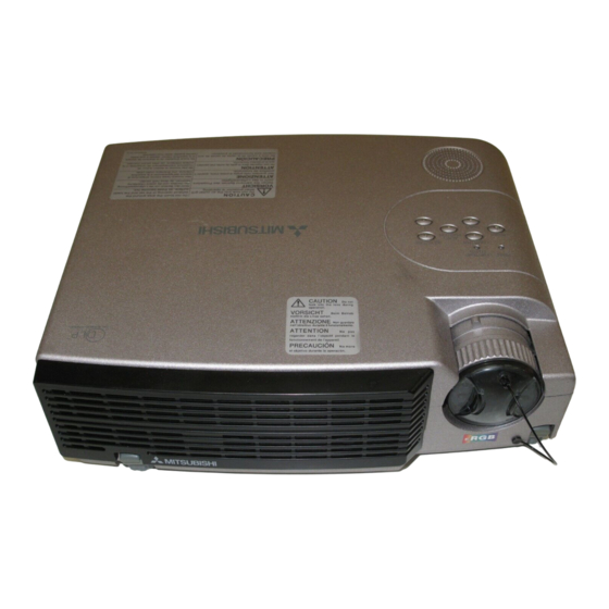
MITSUBISHI
CAUTION
Before servicing this chassis, it is important that the service person reads the "SAFETY PRECAUTIONS" and "PRODUCT
SAFETY NOTICE" in this service manual.
• Power Input
: AC 100~240 V ; 50 / 60 Hz
• Rated Input
: 2.8 A
• LCD Panel
: 0.7 inch DMD device: 1 piece
[SD200U]
Pixels 800 × 600= 480,000 pixels
[XD200U]
Pixels 1,024 × 768= 786,432 pixels
• Colors
: 16,770,000 colors
• Projection Lens
: F 2.5~3.0 f = 23.2~28.4 mm
• Light Source Lamp
: 210 W NSH
• Picture Size
: aspect ratio 4:3 40~300 inch
• PC Compatibility
: [SD200U]
Resolution: 640x400-800x600+Compressed
1024x768
[XD200U]
Resolution: 640x400-1024x768+Compressed
1280x1024
Sync on Green available
• Video Compatibility
: NTSC/NTSC4.43/PAL(including PAL-
M,N)/SECAM, PAL-60 DVD
(Component)/HDTV(1080i)/720p/(525p)
Copyright C 2002 Mitsubishi Electric Corporation All Rights Reserved.
SPECIFICATIONS
MITSUBISHI ELECTRIC
LCD PROJECTOR
DLP1 CHASSIS
MODEL
SD200U/XD200U
• Audio Output
: 2W mono
: 1.57"(4cm) round type (8 Ω 2W), 1 pc.
• Speaker
: Luminance signal: 1.0 V(p-p) 75 Ω (negative sync.)
• S-Video Input
Chroma signal: 0.286 V(p-p) 75 Ω (burst signal)
: 1.0 V(p-p) 75 Ω (negative sync.)
• Video Input
• Audio Input
: 350 mV(rms), 10 kΩ or more
: RGB: 0.7 V(p-p) 75 Ω
• Analog RGB Input
(Mini D-SUB 15P)
YC
C
HD/CS: TTL level (positive or negative)
VD: TTL level (positive or negative)
• Control Connector
: Serial(Mini DIN 9 pin female connector) RS-
232C standards
: 11.8"(W) × 3.5"(H) × 9.6"(D)
• Cabinet Dimensions
(300 × 90 × 245 mm)
(Legs are not included.)
• Weight
: Approx. 6.6 lbs. (3 kg)
• Length of Power Cord
: 114 inch (2.9 m)
• Temperature,Humidity
: 41°F (5
(performance guarantee)
30 to 90%
• Weight and dimensions shown are approximate.
• Design and specifications are subject to change without notice.
C
: 1.0 V (p-p) (Y) (negative sync.)
B
R
C
: 0.7 V (p-p)
B
R
°
C) to 95°F (35
°
C) ,
2002
Advertisement
Table of Contents

Related Manuals for Mitsubishi SD200U


Summary of Contents for Mitsubishi SD200U
-
Page 1: Specifications
° C) , M,N)/SECAM, PAL-60 DVD (performance guarantee) 30 to 90% (Component)/HDTV(1080i)/720p/(525p) • Weight and dimensions shown are approximate. • Design and specifications are subject to change without notice. MITSUBISHI ELECTRIC Copyright C 2002 Mitsubishi Electric Corporation All Rights Reserved. -
Page 2: Table Of Contents
CONTENTS – FILE “COVERPGE” – SPECIFICATIONS ···································································································································· CONTENTS ··········································································································································· – FILE “EXPOSED” – TRADEMARK, REGISTERED TRADEMARK ·························································································· PRODUCT SAFETY NOTICE ·················································································································· SAFETY PRECAUTIONS························································································································· PCBs LOCATION ····································································································································· EXPOSED VIEW ······································································································································ DISASSEMBLY ········································································································································ REMOVAL OF LAMP ······························································································································· LEAD DRESS··········································································································································· PACKING·················································································································································· – FILE “MAINTENA” – LAMP REPLACEMENT····························································································································... -
Page 3: Trademark, Registered Trademark
TRADEMARK, REGISTERED TRADEMARK Apple, Macintosh are registered trademarks of Apple Computer Inc. IBM, VGA, PS/2 are trademarks or registered trademarks of International Business Machines Corporation. Microsoft Windows 95/98/Me are either registered trademarks or trademarks of Microsoft Corporation in the United States and/or other countries. Space Pointer is registered trademarks of ALPS ELECTRIC CO., LTD. -
Page 4: Safety Precautions
SAFETY PRECAUTIONS North America NOTICE: Observe all cautions and safety related notes located inside the cabinet and on the chassis. WARNING 1. Operation of this LCD PROJECTOR outside the cabinet or with the cover removed presents a shock hazard from the LCD PROJECTOR power supplies. -
Page 5: Pcbs Location
PCBs LOCATION Fig. 1 Parts List : See Part List Page 2. Item No. Parts Name LAMP POWER UNIT TERMINAL PCB ASSY IRF PCB ASSY FAN PCB ASSY POWER SUB PCB ASSY FORMATTER PCB ASSY SIGNAL PCB ASSY KEY PCB ASSY IRR PCB ASSY PFC PCB ASSY POWER PCB ASSY... -
Page 6: Exposed View
EXPOSED VIEW LVP ASSY Note: Technicians shall put on the wrist band to protect DLP against Static electricity during the operations. Parts List : See Part List Page 3. Parts Name Number of Screws q Front Grill Unit A x1 w Top Case Assy B x2, C x3, D x1 e Lens B Cover... - Page 7 SIGNAL ASSY A x3 Parts List : See Part List Page 4. Parts Name Number of Screws A x3 q SIGNAL PCB ASSY w Signal B Holder none e Signal A Holder none B x4 r FORMATTER UNIT Number of Screws : The number of Screws holding Parts.
- Page 8 LAMP POWER ASSY Parts List : See Part List Page 4. Parts Name Number of Screws q LAMP POWER PCB ASSY none (2 Hooks) w POWER SUB PCB ASSY none (1 Hook) e FAN PCB ASSY none (1 Hook) r CHASSIS FLAME none Number of Screws : The number of Screws holding Parts.
- Page 9 OPTICAL UNIT Part A x3 B x1 D x1 B x1 C x4 Fig. 2-6 Parts Name Number of Screws A x3 q Color Wheel Assy B x2 w Color Wheel Cover e UVAR Filter - - - C x4 r Lens Unit t Cooling Fan (OPTICAL UNIT) D x1...
-
Page 10: Disassembly
DISASSEMBLY 1. Removal of FRONT GRILL Top Case Assy 1. Remove the (a) screw as shown in Fig. 3-1. 2. Remove the Front Grill as shown in Fig. 3-1. b x1 2. Removal of TOP CASE ASSY 1. Remove the Front Grill following “1. Removal of FRONT GRILL”. - Page 11 4. Removal of POWER PCB ASSY, TERMINAL PCB ASSY and PFC PCB b x3 ASSY Power Assy 1. Remove the Front Grill following “1. Removal of FRONT GRILL”. 2. Remove the Top Case Assy following “2. Removal of TOP CASE ASSY”. 3.
- Page 12 5. Removal of LAMP POWER PCB ASSY, POWER SUB PCB ASSY and FAN PCB LAMP POWER ASSY ASSY 1. Remove the Front Grill following “1. Removal of FRONT GRILL”. 2. Remove the Top Case Assy following “2. Removal of TOP CASE ASSY”. 3.
- Page 13 6. Removal of IRR PCB ASSY IRR PCB ASSY b x1 1. Remove the Front Grill following “1. Removal of FRONT a x2 GRILL”. 2. Remove the Top Case Assy following “2. Removal of TOP CASE ASSY”. Rear Grill Assy 3.
- Page 14 a x7 OPTICAL UNIT Fig. 3-6-2 8. Removal of COOLING FAN (POWER) Cooling Fan (Power) 1. Remove the Front Grill following “1. Removal of FRONT GRILL”. a x1 a x1 2. Remove the Top Case Assy following “2. Removal of TOP CASE ASSY”.
- Page 15 9. Removal of COOLING FAN (DMD) and COOLING FAN (LAMP) 1. Remove the Front Grill following “1. Removal of FRONT Cooling Fan (DMD) GRILL”. 2. Remove the Top Case Assy following “2. Removal of TOP CASE ASSY”. 3. Remove the Rear Grill Assy following “6. Removal of a x1 IRR PCB ASSY”.
-
Page 16: Removal Of Lamp
Removal of Lamp Note: Only service persons are allowed to replace the Lamp Support (U) Lamp. b x2 Power Socket Be careful not to scratch or leave a fingerprint on the Lamp when replacing it. a x1 (Removal) 1. Remove the (a) screw and the Power Socket as shown in Fig. -
Page 17: Lead Dress
LEAD DRESS Note: 1. The inner wires are clamped so that they do not come close to heat generating parts. After servicing route all wires in their original position. 2. Technicians ought to put on the wrist band to protect DLP against Static electricity during the operations. 1. - Page 18 Wire routing around the POWER SUB PCB ASSY cooling fan (POWER) POWER SUB PCB ASSY Fig. 5-2 Wire routing on the TERMINAL PCB ASSY TERMINAL PCB ASSY Terminal plate Fig. 5-3 Wire routing around the Speaker Put the slack in the lead wire (Speaker) on the Cooling fan (DMD) side.
-
Page 19: Packing
PACKING !3 ! 4 ! 5 !6 ! 7 io!0 !1 ! 2 ! 3 Parts List : See Part List Page 7. Item No. Parts Name Packing Cushion T Packing Cushion B Packing Sheet Packing Case Packing Case Soft Case Sheet Instruction Book Quick Reference Card... -
Page 20: Lamp Replacement
LAMP REPLACEMENT When the lamp no longer functions, replace it with a new 7. Put the handle back to the holding Handle one. point. • Make sure that the handle is Caution: locked. • Do not remove the lamp immediately after turning off the 8. -
Page 21: Maintenance
MAINTENANCE Caution: To protect the surface of the projector from fading or Be sure to turn off the projector and unplug the power cord deteriorating: from the wall outlet before you perform any maintenance on • Do not spray insecticide on or inside the projector. the projector. -
Page 22: Function Menu (Setting Menu Only For Service)
FUNCTION MENU ( SETTING MENU ONLY FOR SERVICE ) How to display the FUNCTION menu 1. Select [Language] on the OPTION menu. 2. Press the [ENTER/STILL], [+], and [ENTER/STILL] buttons on the remote control in order, and the FUNCTION menu will be displayed.. -
Page 23: Replacement Of Main Pcb Assy
5. Select the model to use. Select [XD200/SD200] when COM port No. Select the model. Selects the COM port. under connecting using XD200U and SD200U. Exits the application. Read out the factory Ineffective with this Write the factory Ineffective with this adjustment data from model. -
Page 24: Download Of The Firmware
2. Connect the COM port of the PC and the RS-232C terminal of the projector using an RS-232C cable (Service Component). Note: The RS-232C cable is only for SD200U/XD200U. The cables for existing LCD projectors can’t be connected physically. 3. Turn off the main power of projector. -
Page 25: How To Use The Video Mode
HOW TO USE THE VIDEO MODE Outline Troubleshooting • Video mode 1 : Cross color suppression mode If the signal supplied to the VIDEO input isn’t displayed This is the default video mode. Use this correctly, check the followings. mode for movies. •... -
Page 26: About Laser Beam
ABOUT LASER BEAM 1 Transmitter indicator 2 Power button 3 COMPUTER button 4 Mouse button 5 Right click button (For mouse) POWER MUTE 6 MENU button COMPUTER VIDEO 7 AUTO POSITION button 8 KEYSTONE button MOUSE LASER 9 + , - (KEYSTONE / VOLUME) buttons 10 EXPAND button 11 PinP button 12 ENTER / STILL button... -
Page 27: Electrical Adjustments
Personal • Monitor for Personal Computer COMPUTER IN Computer Terminal • RS-232C Cable (Service Component) RS-232C Cable • SVGA Signal Generator (Equivalent to VG-812) [SD200U] Signal • XGA Signal Generator (Equivalent to VG-812) [XD200U] Personal Generator this PROJECTOR Computer • Red Scale signal (for C/W Delay adjustment) - Page 28 Adjustment with Microsoft ® Windows ® 95/98/Me Operating System 1. Starting 1. Start Windows 95/98/Me. 2. Double click [Accessories] folder. 3. Double click [Hyper Terminal] folder. 4. Double click [HyperTrm] icon. 2. Hyper Terminal Setting 1. Click [Properties] in File menu on the Hyper Item Setting Terminal window.
- Page 29 5. Enter [00 ~ 5] (A/D adjustment command) to the Hyper Terminal window and Model Signal automatic adjustment will start. SD200U SVGA 6. The return command [00 ~ 5111] is displayed on the Hyper Terminal Window XD200U after the adjustment. The last 3 figures of the return command indicate the result of adjustment and each figure corresponds to R, G, and B.
- Page 30 7. The newly entered value is saved automatically. Press the [MENU] button to exit the FUNCTION menu. * In the SVGA model (SD200U), flicker may appear when the C/W delay is adjusted to a certain value. This is unique to this model. Carry out the following procedure to prevent flicker and change the C/W delay setting to a value at which the colors of the red scale signal are displayed properly and no flicker appears.
- Page 31 3. Start the communication program [Hyper Terminal] in Microsoft Windows Model Signal 95/98/Me to open the window. (For setting, refer to Hyper Terminal setting on SD200U SVGA P.2) XD200U 4. Set the following items on the picture menu. Table 1 CONTRAST .
- Page 32 [Video Signal Circuit] Adjustment purpose The best white balance of picture. (PC Phase) 4. White Balance (PC Phase) Symptom when Monochrome picture has a color tint. incorrectly adjusted Measuring *Make this adjustment after performing 3. White balance (sRGB). instrument *Make this adjustment only when a monochrome picture has color tints remarkably.
-
Page 33: Diagnosis Information
DIAGNOSIS INFORMATION Outline of self-diagnosis function This product is provided with the self-diagnosis function. In case of any abnormality, the LED at the top of the product will indicate the errors. There are 2 ways for diagnosis. 1 Connect a personal computer to the product. Then, input [00 ~ CHK] from the hyper-terminal window of the personal computer during stand-by. - Page 34 LED Indication Check Point Preferen- Symptom Failure Reset tial order POWER LAMP Reference Red/Green Main Green No power-on IIC bus failure of EEPROM SIGNAL IC402 (SCL, SDA) alternately Power IC4A3 (SW3.3), Red/Green Main Orange No power-on SW3.3 or SW5A SIGNAL alternately Power IC4A4 (SW5)
- Page 35 LED Indication Check Point Preferen- Symptom Failure Reset tial order POWER LAMP Reference No power-on Lamp turn to off during power-on SIGNAL SA connector Auto for one minute Green flash 2 No power-on Lamp explosion Lamp explosion Manual for one minute Computer Red/Green Green...
-
Page 36: Diagnostic Software, To Read Warning History ( Pcgc8 Ver.2 )
Select [XD200U] Note: When the power is turned off because of any error, when using XD200U and SD200U. the warning history data are saved. Or, only when an error occurs during power on or when an error is detected during self-diagnosis (or immediately after pressing the DIAGNOSIS button), the warning history data are saved. - Page 37 (3) Warning dialog window (4) Switching the COM port 1. The warning dialog window displays the error location. 1. Select the serial port to which the cable is being 2. “ERROR TIME (SET TIME)” displays the time when the connected. When the selected serial port isn’t available warning history data has been saved (the SET TIME in or doesn’t exist, an error message window is displayed.
-
Page 38: Specification Of Rgb Signals In Each Computer Mode Of The Projector
SPECIFICATION OF RGB SIGNALS IN EACH COMPUTER MODE OF THE PROJECTOR [SD200U] resolution horizontal Vertical Normal mode Real mode Signal mode (H x V) frequency (kHz) frequency (Hz) (H x V) (H x V) TV60 15.73 59.94 800 x 600 TV50 15.63... - Page 39 [XD200U] resolution horizontal Vertical Normal mode Real mode Signal mode (H x V) frequency (kHz) frequency (Hz) (H x V) (H x V) TV60 15.73 59.94 1024 x 768 TV50 15.63 50.00 1024 x 768 525p 31.47 59.94 1024 x 768 1080i 33.75 60.00...
-
Page 40: Diagnosis Flow Chart
DIAGNOSIS FLOW CHART Image system Is the lamp lit? Is the indication on LED normal after POWER ON? (POWER : Green, LAMP/TEMP/STATUS : Green) An image is not projected properly. Is the proper video signal inputted? Or is the image projected correctly? Malfunction of IC400 or subsequent circuits Check the voltage waveform of connector Check the video signal circuit around IC400... - Page 41 Power source system 1 LED is not lit. (The product does not enter the stand-by mode.) Check the failure on the PCB- Has the POWER, then replace the parts FUSE (F900) blown? such as D900, Q900, etc. Is the lead wire to Replace the lead wire.
- Page 42 Power source system 2 When the stand-by power source is abnormal. Are RD and SD Insert or replace them. connectors OK? Pull out the RD connector of RD-SD Is the pin No. 1 of the Check the circuit around D9A0 RD connector -6V? Abnormal video or audio.
- Page 43 Power source system 3 The lamp does not light. Are CN1 (PCB POWER, LAMP POWER UNIT) and Insert or replace them. SA-CN2 (PCB SIGNAL, LAMP POWER UNIT) connectors OK? Are the pins No. 1 Malfunction of LAMP POWER UNIT. to 6 of the PB connector 370V? Are the pins No.
-
Page 44: Parts List
PARTS LIST MODEL : SD200U/XD200U In order to expedite delivery of replacement part orders. Specify : 1. Model number/Serial number 2. Part number and Description 3. Quantity Unless full information is supplied,delay in execution of orders will result. : Warranty return items... - Page 45 The PARTS on this page correspond to ones on page 3 in the EXPOSED file. ITEM PARTS NO. PARTS NAME DESCRIPTION PCBs LOCATION * ! 1 939P901O10 LAMP POWER UNIT * ! 2 934C008O01 TERMINAL PCB ASSY * ! 3 935D679O01 IRF PCB ASSY * ! 4...
- Page 46 The PARTS on this page correspond to ones on page 4 in the EXPOSED file. ITEM PARTS NO. PARTS NAME DESCRIPTION EXPOSED VIEW LVP ASSY (Fig. 2-1) 761B391O30 FRONT GRILL UNIT 761B391O10 FRONT GRILL UNIT 710A120O30 TOP CASE ASSY - - - - - LENS B COVER - - - - - LENS B COVER...
- Page 47 The PARTS on this page correspond to ones on page 5 in the EXPOSED file. ITEM PARTS NO. PARTS NAME DESCRIPTION EXPOSED VIEW SIGNAL ASSY (Fig. 2-2) * ! 1 935A110O02 SIGNAL PCB ASSY * ! 1 935A110O01 SIGNAL PCB ASSY - - - - - SIGNAL B HOLDER - - - - -...
- Page 48 The PARTS on this page correspond to ones on page 6 and page 7 in the EXPOSED file. ITEM PARTS NO. PARTS NAME DESCRIPTION EXPOSED VIEW LAMP POWER ASSY (Fig. 2-4) - - - - - LAMP POWER PCB ASSY * ! 2 939P901O10 LAMP POWER UNIT...
- Page 49 The PARTS on this page correspond to ones on page 17 in the EXPOSED file. ITEM PARTS NO. PARTS NAME DESCRIPTION PACKING 803A587O10 PACKING CUSHION T 803A588O10 PACKING CUSHION B 831D190O90 PACKING SHEET CP-GZ1 802B830O30 PACKING CASE 802B830O10 PACKING CASE - - - - - PACKING CASE 772P037O10...
- Page 50 ELECTRICAL PARTS AND OTHERS SYMBOL PARTS SYMBOL PARTS PARTS NAME DESCRIPTION PARTS NAME DESCRIPTION INTEGRATED CIRCUITS TRANSISTORS IC200 275P779O10 MOS IC FL12200 Q300 260P855O90 CHIP TRANSISTOR 2SD1819A-S IC201 275P809O10 MOS IC NC7SZ14P5X Q301 260P855O90 CHIP TRANSISTOR 2SD1819A-S IC202 275P124O10 MOS IC HD74LVC245AT Q302 260P872O20 CHIP TRANSISTOR...
- Page 51 SYMBOL PARTS SYMBOL PARTS PARTS NAME DESCRIPTION PARTS NAME DESCRIPTION D2F5 262P802O10 DIODE 1SS302 D300 262P802O10 DIODE 1SS302 FILTERS D301 262P802O10 DIODE 1SS302 D302 262P802O10 DIODE 1SS302 L200 409P777O80 EMI FILTER BLM21P221S D303 262P802O10 DIODE 1SS302 L202 409P865O20 EMI FILTER BLM11A601S L203 409P865O20 EMI FILTER...
- Page 52 SYMBOL PARTS SYMBOL PARTS PARTS NAME DESCRIPTION PARTS NAME DESCRIPTION R236 103P500O50 CHIP RESISTOR 1/16W 22Ω-J L4E5 409P865O20 EMI FILTER BLM11A601S R237 103P500O50 CHIP RESISTOR 1/16W 22Ω-J L500 409P865O20 EMI FILTER BLM11A601S R240 103P500O90 CHIP RESISTOR 1/20W 47Ω-J L501 409P865O20 EMI FILTER BLM11A601S R250 103P509O50 CHIP RESISTOR...
- Page 53 SYMBOL PARTS SYMBOL PARTS PARTS NAME DESCRIPTION PARTS NAME DESCRIPTION R339 103P496O50 CHIP METAL RESISTOR 1/16W 47kΩ-F R4A2 103P502O90 CHIP RESISTOR 1/16W 2.2kΩ-J R340 103P502O10 CHIP RESISTOR 1/16W 470Ω-J R341 103P504O30 CHIP RESISTOR 1/16W 33kΩ-J R4A4 103P503O70 CHIP RESISTOR 1/16W 10kΩ-J R4A5 103P502O70 CHIP RESISTOR 1/16W 1.5kΩ-J...
- Page 54 SYMBOL PARTS SYMBOL PARTS PARTS NAME DESCRIPTION PARTS NAME DESCRIPTION R604 103P500O50 CHIP RESISTOR 1/16W 22Ω-J R9B1 103P491O80 CHIP METAL RESISTOR 1/16W 510Ω-F R605 103P501O00 CHIP RESISTOR 1/16W 56Ω-J R9B2 103P491O50 CHIP METAL RESISTOR 1/16W 390Ω-F R605 103P500O50 CHIP RESISTOR 1/16W 22Ω-J R9W0 103P502O30 CHIP RESISTOR 1/16W 680Ω-J...
- Page 55 SYMBOL PARTS SYMBOL PARTS PARTS NAME DESCRIPTION PARTS NAME DESCRIPTION C2F8 141P142O10 CHIP CAPACITOR B25V 0.01µF-K C215 141P144O20 CHIP CAPACITOR F16V 0.1µF-Z C2F9 181P520O30 CHIP ELE CAPACITOR 6.3V 4.7µF-M C216 141P144O20 CHIP CAPACITOR F16V 0.1µF-Z C2G0 141P142O10 CHIP CAPACITOR B25V 0.01µF-K C217 141P144O20 CHIP CAPACITOR F16V 0.1µF-Z...
- Page 56 SYMBOL PARTS SYMBOL PARTS PARTS NAME DESCRIPTION PARTS NAME DESCRIPTION C429 141P144O20 CHIP CAPACITOR F16V 0.1µF-Z C430 141P144O20 CHIP CAPACITOR F16V 0.1µF-Z C4E8 181P522O30 CHIP ELE CAPACITOR 16V 10µF-M C4E9 141P144O20 CHIP CAPACITOR F16V 0.1µF-Z C431 141P144O20 CHIP CAPACITOR F16V 0.1µF-Z C500 141P144O60 CHIP CAPACITOR F16/10V 1µF-Z...
- Page 57 SYMBOL PARTS SYMBOL PARTS PARTS NAME DESCRIPTION PARTS NAME DESCRIPTION C664 141P144O60 CHIP CAPACITOR F16/10V 1µF-Z C9W3 141P135O60 CHIP CAPACITOR F16V 2.2µF-Z C665 141P144O20 CHIP CAPACITOR F16V 0.1µF-Z C9W4 181P522O60 CHIP ELE CAPACITOR 16V 47µF-M C666 141P144O20 CHIP CAPACITOR F16V 0.1µF-Z C667 141P144O20 CHIP CAPACITOR F16V 0.1µF-Z...
- Page 58 SYMBOL PARTS SYMBOL PARTS PARTS NAME DESCRIPTION PARTS NAME DESCRIPTION J2F3 449C145O10 MINI DIN SOCKET J300 451C104O10 HEADPHONE JACK BLACK 499D035O20 UVAR FILTER J301 451C104O10 HEADPHONE JACK BLACK 683D048O10 WASHER 0.45X4.3X8.5 669D329O30 SCREW (D900) M3X0.5-10 J302 451C104O10 HEADPHONE JACK BLACK 669D329O30 SCREW (D902) M3X0.5-10 J330...
- Page 59 TRADEMARK, REGISTERED TRADEMARK Apple, Macintosh are registered trademarks of Apple Computer Inc. IBM, VGA, PS/2 are trademarks or registered trademarks of International Business Machines Corporation. Microsoft Windows 95 is a registered trademark of Microsoft in the U.S. and other countries. Space Pointer is registered trademarks of ALPS ELECTRIC CO., LTD.
-
Page 60: Leakage Current Check
SAFETY PRECAUTIONS North America NOTICE: Observe all cautions and safety related notes located inside the cabinet and on the chassis. WARNING 1. Operation of this LCD PROJECTOR outside the cabinet or with the cover removed presents a shock hazard from the LCD PROJECTOR power supplies. - Page 61 PCBs LOCATION Fig. 1 Parts List : See Part List Page 2. Item No. Parts Name LAMP POWER UNIT TERMINAL PCB ASSY IRF PCB ASSY FAN PCB ASSY POWER SUB PCB ASSY FORMATTER PCB ASSY SIGNAL PCB ASSY KEY PCB ASSY IRR PCB ASSY PFC PCB ASSY POWER PCB ASSY...
- Page 62 EXPOSED VIEW LVP ASSY Note: Technicians shall put on the wrist band to protect DLP against Static electricity during the operations. Parts List : See Part List Page 3. Parts Name Number of Screws q Front Grill Unit A x1 w Top Case Assy B x2, C x3, D x1 e Lens B Cover...
- Page 63 SIGNAL ASSY A x3 Parts List : See Part List Page 4. Parts Name Number of Screws A x3 q SIGNAL PCB ASSY w Signal B Holder none e Signal A Holder none B x4 r FORMATTER UNIT Number of Screws : The number of Screws holding Parts.
- Page 64 LAMP POWER ASSY Parts List : See Part List Page 4. Parts Name Number of Screws q LAMP POWER PCB ASSY none (2 Hooks) w POWER SUB PCB ASSY none (1 Hook) e FAN PCB ASSY none (1 Hook) r CHASSIS FLAME none Number of Screws : The number of Screws holding Parts.
- Page 65 OPTICAL UNIT Part A x3 B x1 D x1 B x1 C x4 Fig. 2-6 Parts Name Number of Screws A x3 q Color Wheel Assy B x2 w Color Wheel Cover e UVAR Filter - - - C x4 r Lens Unit t Cooling Fan (OPTICAL UNIT) D x1...
- Page 66 DISASSEMBLY 1. Removal of FRONT GRILL Top Case Assy 1. Remove the (a) screw as shown in Fig. 3-1. 2. Remove the Front Grill as shown in Fig. 3-1. b x1 2. Removal of TOP CASE ASSY 1. Remove the Front Grill following “1. Removal of FRONT GRILL”.
- Page 67 4. Removal of POWER PCB ASSY, TERMINAL PCB ASSY and PFC PCB b x3 ASSY Power Assy 1. Remove the Front Grill following “1. Removal of FRONT GRILL”. 2. Remove the Top Case Assy following “2. Removal of TOP CASE ASSY”. 3.
- Page 68 5. Removal of LAMP POWER PCB ASSY, POWER SUB PCB ASSY and FAN PCB LAMP POWER ASSY ASSY 1. Remove the Front Grill following “1. Removal of FRONT GRILL”. 2. Remove the Top Case Assy following “2. Removal of TOP CASE ASSY”. 3.
- Page 69 6. Removal of IRR PCB ASSY IRR PCB ASSY b x1 1. Remove the Front Grill following “1. Removal of FRONT a x2 GRILL”. 2. Remove the Top Case Assy following “2. Removal of TOP CASE ASSY”. Rear Grill Assy 3.
- Page 70 a x7 OPTICAL UNIT Fig. 3-6-2 8. Removal of COOLING FAN (POWER) Cooling Fan (Power) 1. Remove the Front Grill following “1. Removal of FRONT GRILL”. a x1 a x1 2. Remove the Top Case Assy following “2. Removal of TOP CASE ASSY”.
- Page 71 9. Removal of COOLING FAN (DMD) and COOLING FAN (LAMP) 1. Remove the Front Grill following “1. Removal of FRONT Cooling Fan (DMD) GRILL”. 2. Remove the Top Case Assy following “2. Removal of TOP CASE ASSY”. 3. Remove the Rear Grill Assy following “6. Removal of a x1 IRR PCB ASSY”.
- Page 72 Removal of Lamp Note: Only service persons are allowed to replace the Lamp Support (U) Lamp. b x2 Power Socket Be careful not to scratch or leave a fingerprint on the Lamp when replacing it. a x1 (Removal) 1. Remove the (a) screw and the Power Socket as shown in Fig.
- Page 73 LEAD DRESS Note: 1. The inner wires are clamped so that they do not come close to heat generating or high voltage parts. After servicing route all wires in their original position. 2. Technicians shall put on the wrist band to protect LCD against Static electricity during the operations. 1.
- Page 74 Wire routing around the POWER SUB PCB ASSY cooling fan (POWER) POWER SUB PCB ASSY Fig. 5-2 Wire routing on the TERMINAL PCB ASSY TERMINAL PCB ASSY Terminal plate Fig. 5-3 Wire routing around the Speaker Put the slack in the lead wire (Speaker) on the Cooling fan (DMD) side.
- Page 75 PACKING !3 ! 4 ! 5 !6 ! 7 io!0 !1 ! 2 ! 3 Parts List : See Part List Page 7. Item No. Parts Name Packing Cushion T Packing Cushion B Packing Sheet Packing Case Packing Case Soft Case Sheet Instruction Book Quick Reference Card...
- Page 76 PARTS LIST MODEL : SD200U/XD200U In order to expedite delivery of replacement part orders. Specify : 1. Model number/Serial number 2. Part number and Description 3. Quantity Unless full information is supplied,delay in execution of orders will result. : Warranty return items...
- Page 77 The PARTS on this page correspond to ones on page 3 in the EXPOSED file. ITEM PARTS NO. PARTS NAME DESCRIPTION PCBs LOCATION * ! 1 939P901O10 LAMP POWER UNIT * ! 2 934C008O01 TERMINAL PCB ASSY * ! 3 935D679O01 IRF PCB ASSY * ! 4...
- Page 78 The PARTS on this page correspond to ones on page 4 in the EXPOSED file. ITEM PARTS NO. PARTS NAME DESCRIPTION EXPOSED VIEW LVP ASSY (Fig. 2-1) 761B391O30 FRONT GRILL UNIT 761B391O10 FRONT GRILL UNIT 710A120O30 TOP CASE ASSY - - - - - LENS B COVER - - - - - LENS B COVER...
- Page 79 The PARTS on this page correspond to ones on page 5 in the EXPOSED file. ITEM PARTS NO. PARTS NAME DESCRIPTION EXPOSED VIEW SIGNAL ASSY (Fig. 2-2) * ! 1 935A110O02 SIGNAL PCB ASSY * ! 1 935A110O01 SIGNAL PCB ASSY - - - - - SIGNAL B HOLDER - - - - -...
- Page 80 The PARTS on this page correspond to ones on page 6 and page 7 in the EXPOSED file. ITEM PARTS NO. PARTS NAME DESCRIPTION EXPOSED VIEW LAMP POWER ASSY (Fig. 2-4) - - - - - LAMP POWER PCB ASSY * ! 2 939P901O10 LAMP POWER UNIT...
- Page 81 DESCRIPTION PACKING 803A587O10 PACKING CUSHION T 803A588O10 PACKING CUSHION B 831D190O90 PACKING SHEET CP-GZ1 802B830O30 PACKING CASE [SD200U] 802B830O10 PACKING CASE [XD200U] - - - - - PACKING CASE 772P037O10 SOFT CASE - - - - - SHEET 871D349O10 INSTRUCTION BOOK...
- Page 82 ELECTRICAL PARTS AND OTHERS SYMBOL PARTS SYMBOL PARTS PARTS NAME DESCRIPTION PARTS NAME DESCRIPTION INTEGRATED CIRCUITS TRANSISTORS IC200 275P779O10 MOS IC FL12200 Q300 260P855O90 CHIP TRANSISTOR 2SD1819A-S IC201 275P809O10 MOS IC NC7SZ14P5X Q301 260P855O90 CHIP TRANSISTOR 2SD1819A-S IC202 275P124O10 MOS IC HD74LVC245AT Q302 260P872O20 CHIP TRANSISTOR...
- Page 83 SYMBOL PARTS SYMBOL PARTS PARTS NAME DESCRIPTION PARTS NAME DESCRIPTION D2F5 262P802O10 DIODE 1SS302 D300 262P802O10 DIODE 1SS302 FILTERS D301 262P802O10 DIODE 1SS302 D302 262P802O10 DIODE 1SS302 L200 409P777O80 EMI FILTER BLM21P221S D303 262P802O10 DIODE 1SS302 L202 409P865O20 EMI FILTER BLM11A601S L203 409P865O20 EMI FILTER...
- Page 84 SYMBOL PARTS SYMBOL PARTS PARTS NAME DESCRIPTION PARTS NAME DESCRIPTION R236 103P500O50 CHIP RESISTOR 1/16W 22Ω-J L4E5 409P865O20 EMI FILTER BLM11A601S R237 103P500O50 CHIP RESISTOR 1/16W 22Ω-J L500 409P865O20 EMI FILTER BLM11A601S R240 103P500O90 CHIP RESISTOR 1/20W 47Ω-J L501 409P865O20 EMI FILTER BLM11A601S R250 103P509O50 CHIP RESISTOR...
- Page 85 SYMBOL PARTS SYMBOL PARTS PARTS NAME DESCRIPTION PARTS NAME DESCRIPTION R339 103P496O50 CHIP METAL RESISTOR 1/16W 47kΩ-F R4A2 103P502O90 CHIP RESISTOR 1/16W 2.2kΩ-J R340 103P502O10 CHIP RESISTOR 1/16W 470Ω-J R341 103P504O30 CHIP RESISTOR 1/16W 33kΩ-J R4A4 103P503O70 CHIP RESISTOR 1/16W 10kΩ-J R4A5 103P502O70 CHIP RESISTOR 1/16W 1.5kΩ-J...
- Page 86 SYMBOL PARTS SYMBOL PARTS PARTS NAME DESCRIPTION PARTS NAME DESCRIPTION R604 103P500O50 CHIP RESISTOR 1/16W 22Ω-J R9B1 103P491O80 CHIP METAL RESISTOR 1/16W 510Ω-F R605 103P501O00 CHIP RESISTOR 1/16W 56Ω-J R9B2 103P491O50 CHIP METAL RESISTOR 1/16W 390Ω-F R605 103P500O50 CHIP RESISTOR 1/16W 22Ω-J R9W0 103P502O30 CHIP RESISTOR 1/16W 680Ω-J...
- Page 87 SYMBOL PARTS SYMBOL PARTS PARTS NAME DESCRIPTION PARTS NAME DESCRIPTION C2F8 141P142O10 CHIP CAPACITOR B25V 0.01µF-K C215 141P144O20 CHIP CAPACITOR F16V 0.1µF-Z C2F9 181P520O30 CHIP ELE CAPACITOR 6.3V 4.7µF-M C216 141P144O20 CHIP CAPACITOR F16V 0.1µF-Z C2G0 141P142O10 CHIP CAPACITOR B25V 0.01µF-K C217 141P144O20 CHIP CAPACITOR F16V 0.1µF-Z...
- Page 88 SYMBOL PARTS SYMBOL PARTS PARTS NAME DESCRIPTION PARTS NAME DESCRIPTION C429 141P144O20 CHIP CAPACITOR F16V 0.1µF-Z C430 141P144O20 CHIP CAPACITOR F16V 0.1µF-Z C4E8 181P522O30 CHIP ELE CAPACITOR 16V 10µF-M C4E9 141P144O20 CHIP CAPACITOR F16V 0.1µF-Z C431 141P144O20 CHIP CAPACITOR F16V 0.1µF-Z C500 141P144O60 CHIP CAPACITOR F16/10V 1µF-Z...
- Page 89 SYMBOL PARTS SYMBOL PARTS PARTS NAME DESCRIPTION PARTS NAME DESCRIPTION C664 141P144O60 CHIP CAPACITOR F16/10V 1µF-Z C9W3 141P135O60 CHIP CAPACITOR F16V 2.2µF-Z C665 141P144O20 CHIP CAPACITOR F16V 0.1µF-Z C9W4 181P522O60 CHIP ELE CAPACITOR 16V 47µF-M C666 141P144O20 CHIP CAPACITOR F16V 0.1µF-Z C667 141P144O20 CHIP CAPACITOR F16V 0.1µF-Z...
- Page 90 SYMBOL PARTS SYMBOL PARTS PARTS NAME DESCRIPTION PARTS NAME DESCRIPTION J2F3 449C145O10 MINI DIN SOCKET J300 451C104O10 HEADPHONE JACK BLACK 499D035O20 UVAR FILTER J301 451C104O10 HEADPHONE JACK BLACK 683D048O10 WASHER 0.45X4.3X8.5 669D329O30 SCREW (D900) M3X0.5-10 J302 451C104O10 HEADPHONE JACK BLACK 669D329O30 SCREW (D902) M3X0.5-10 J330...
-
Page 91: Ic Block Diagrams
IC BLOCK DIAGRAMS PCB-SIGNAL(1/4) IC540 M52036SP CLAMP CLAMP DIGITAL TIMING V.POL. H.POL. VERT S/S IN IC560,IC561 NC7SZ14P5X CLAMP EDGE GEN. FUNCTION TABLE V.SYNC Inputs Outputs LOGIC SEP. LOGIC SYNC H = HIGH Logic Level SEP. L = LOW Logic Level HOR. - Page 92 PCB-SIGNAL(2/4) IC202,IC203,IC204 HD74LVC245T TRUTH TABLE B DATA A DATA A DATA B DATA IC201 NC7SZ14P5X ISOLATION FUNCTION TABLE : HIGH LEVEL : LOW LEVEL : DON'T CARE Inputs Outputs DATA PORT DATA PORT H = HIGH Logic Level L = LOW Logic Level IC270 ICS570B Voltage Output...
- Page 93 IC240 MT48LC2M32B2-6 CONTROL LOGIC BANK3 BANK2 BANK1 CAS# BANK0 COMMAND RAS# DECODE MODE REGISTER REFRESH BANK0 COUNTER ROW- BANK0 ROW- ADDRESS MEMORY ADDRESS LATCH 2048 ARRAY & (2,048x256x32) DECODER DQM0 SENSE AMPLIFIERS DQM3 2048 DATA OUTPUT REGISTER I/O GATING DQM MASK LOGIC READ DATA LATCH DQ31 WRITE DRIVERS...
- Page 94 PCB-SIGNAL(3/4) IC401 MT28F800B3WG-10T@XD200 BYTE# CONTROL LOGIC INPUT 16KB BOOT BLOCK BUFFER ADDR. 8KB PARAMETER BLOCK A18/ BUFFER/ 8KB PARAMETER BLOCK (A19) LATCH INPUT 96KB MAIN BLOCK BUFFER ADDR. POWER 128KB MAIN BLOCK COUNTER (CURRENT) CONTROL 128KB MAIN BLOCK INPUT BUFFER 128KB MAIN BLOCK DQ15/ INPUT DATA...
- Page 95 XFR TO INPUT PROTECTION - ALL LOGIC INPUTS SHIFT REG MSB FIRST A GND *Some of these functions/plns are not avallable with other options. IC408 ICS301M-62(XD200U) IC409 NC7SZ02P5X ICS301M-66(SD200U) VDD GND Clock Output Synthesis Buffer with PLL and Control Divider...
- Page 96 PCB-SIGNAL(4/4) IC4A2 74VHCT541AMTC IC4A5 PCA9540DP POWER-on Reset Input I C-Bus Filter Control TRUTH TABLE Inputs Output H = High Voltage Level PCB-TERMINAL L = Low Voltage Level Z = Higt Impedance X = Immaterial IC2F0 M52055FP IC300 MC74VHC4052DTR2 IN1B IN1A GND1 OUT1 IN2B...
- Page 97 IC500 24LC21TSN IC333 µPC4570G2 VCLK OUT1 HV GENERATOR OUT2 MEMORY EEPROM ARRAY CONTROL CONTROL XDEC LOGIC LOGIC PAGE LATCHES YDEC SENSE AMP IC501,IC502 NC7SZ157P6X R/W CONTROL IC503 HD74LVC14T FUNCTION TABLE Inputs Outputs FUNCTION TABLE Z=(I )·(S)+(I )·(S) INPUT OUTPUT H = HIGH Logic Level L = LOW Logic Level IC600 AD8183ARU IN0 A...
- Page 98 PCB-PFC IC9000 FA5332M SYNC ON/OFF 10µ A ON/OFF BIAS UVLO BIAS Dmax PWM COMP ER.AMP CURR.AMP Vocp IDET VDET...
- Page 99 SCHEMATIC DIAGRAMS MODEL : SD200U XD200U NOTE 1. TP6A, etc. show Test Points. 2. Capacitors pF, for numbers more than 1 Value Not indicated µF, for numbers less than 1 Dielectric Not indicated : 50V Strength ± 10 % Not indicated =...
- Page 100 R561 L2A5 C2E1 SCL-SW SDA-SW STBY5A STBYR6 RESZ-AD SSEN1 SSEN2 VZ/PC V1Z/V2 P1Z/P2 SD200U/XD200U CONTENTS BLOCK DIAGRAM •••••• q POWER SUB •••••• u AD/DEC-SIGNAL(1/4) •••••• w •••••• u IP-SIGNAL (2/4) •••••• e •••••• u •••••• r •••••• u SCALER-SIGNAL (3/4) GA-SIGNAL (4/4) ••••••...
- Page 101 C262 R250 R251 DKATR IC203 IC204 R252 R240 SDA-SW SCL-SW R241 SDA-SW SCL-SW SD200U/XD200U CONTENTS BLOCK DIAGRAM •••••• q POWER SUB •••••• u AD/DEC-SIGNAL(1/4) •••••• w •••••• u IP-SIGNAL (2/4) •••••• e •••••• u •••••• r •••••• u SCALER-SIGNAL (3/4) GA-SIGNAL (4/4) ••••••...
- Page 102 TPDG0 TPDG1 TPDG2 TPDG3 R412 IC408 R431 R413 R414 R415 C438 L418 DCLK SD200U/XD200U CONTENTS BLOCK DIAGRAM •••••• q POWER SUB •••••• u AD/DEC-SIGNAL(1/4) •••••• w •••••• u IP-SIGNAL (2/4) •••••• e •••••• u •••••• r •••••• u SCALER-SIGNAL (3/4) GA-SIGNAL (4/4) ••••••...
- Page 103 R4E4 C4B8 C4B9 PWMF1 R4E5 PWMF2 KEYPWR KEYCOM KEYVID KEYAUT KEYKS+ KEYKS- GAERR SD200U/XD200U CONTENTS BLOCK DIAGRAM •••••• q POWER SUB •••••• u AD/DEC-SIGNAL(1/4) •••••• w •••••• u IP-SIGNAL (2/4) •••••• e •••••• u •••••• r •••••• u SCALER-SIGNAL (3/4) GA-SIGNAL (4/4) ••••••...
- Page 104 R2F4 C348 R2G6 C2G3 Q331 R347 Q330 R2F5 R348 L2F5 J2F3 D2F5 C2G1 SD200U/XD200U CONTENTS BLOCK DIAGRAM •••••• q POWER SUB •••••• u AD/DEC-SIGNAL(1/4) •••••• w •••••• u IP-SIGNAL (2/4) •••••• e •••••• u •••••• r •••••• u SCALER-SIGNAL (3/4) GA-SIGNAL (4/4) ••••••...
- Page 105 L9A9 Q9A2 R9A13 Q9A1 C9A16 PC951 R964 R963 Q9A0 R9A10 R9A11 PC952 C9A17 SD200U/XD200U CONTENTS BLOCK DIAGRAM •••••• q POWER SUB •••••• u AD/DEC-SIGNAL(1/4) •••••• w •••••• u IP-SIGNAL (2/4) •••••• e •••••• u •••••• r •••••• u SCALER-SIGNAL (3/4) GA-SIGNAL (4/4) ••••••...
- Page 106 A – 3 Q601 A – 3 R611 A – 3 C614 A – 2 IC503 B – 3 Q603 A – 3 R612 A – 3 C615 A – 2 IC600 A – 3 R613 A – 3 SD200U XD200U...
- Page 107 C905 C903 C9W7 C – 1 E – 1 R9B3 B – 3 D9A2 A – 1 Q702 A – 3 Z900 D – 3 C905 R903 C903 R900 R900 C902 C900 R905 R905 LIVE D900 D900 LIVE SD200U XD200U...