
Texas Instruments CC2538 Manuals
Manuals and User Guides for Texas Instruments CC2538. We have 3 Texas Instruments CC2538 manuals available for free PDF download: User Manual, Quick Start Manual

Texas Instruments CC2538 User Manual (781 pages)
System-on-Chip Solution for 2.4-GHz IEEE 802.15.4 and ZigBee/ZigBee IP Applications
Brand: Texas Instruments
|
Category: Switch
|
Size: 4 MB
Table of Contents
-
-
Preface26
-
-
Overview33
-
-
-
Memory Map36
-
Flash Memory37
-
Mpu37
-
Sram37
-
Radio38
-
Rom38
-
CCP Pins39
-
MAC Timer39
-
Sleep Timer39
-
Uart41
-
Usb41
-
I 2 C42
-
Analog43
-
Ssi43
-
Adc44
-
-
Interrupts47
-
Faults75
-
Memory Map157
-
-
Bit-Banding161
-
-
Bit-Band Mapping163
-
Data Storage164
-
Interrupts166
-
Exception Model167
-
Exception States167
-
Exception Types167
-
Interrupts169
-
Vector Table172
-
-
-
Vector Table173
-
-
Fault Handling176
-
-
JTAG Interface179
-
-
Debug Port180
-
-
-
-
System Control186
-
Power Management187
-
-
-
Internal Memory
217-
Chapter 8
218-
Flash Write218
-
Introduction218
-
-
CPU Flash Write221
-
-
-
Flash Mass Erase225
-
-
-
ROM Sub System227
-
Sram227
-
-
I/O Control235
-
Gpio236
-
-
-
Data Control237
-
-
-
Pad Control240
-
Configuration241
-
-
-
Priority294
-
-
-
Single Request295
-
-
-
Transfer Modes296
-
Basic Mode297
-
-
-
Timer Modes327
-
-
PWM Mode330
-
-
Watchdog Timer376
-
-
Watchdog Timer377
-
-
-
Introduction388
-
Crc16389
-
-
-
Introduction392
-
-
-
LIN Support399
-
-
LIN Message399
-
-
Bit UART Mode400
-
Interrupts401
-
-
-
Block Diagram423
-
-
-
Receive FIFO425
-
-
DMA Operation431
-
-
Examples of I445
-
-
Arbitration445
-
-
-
Usb Controller
464-
Chapter 21
465-
48-Mhz USB PLL465
-
USB Enable465
-
USB Introduction465
-
-
USB Interrupts466
-
-
-
USB Reset467
-
-
Endpoint 0468
-
Read Requests470
-
-
Error Conditions474
-
-
-
Endpoints 1-5482
-
-
-
FIFO Management483
-
FIFO Access484
-
-
IN/OUT Fifos483
-
-
Dma492
-
Remote Wake-Up492
-
-
Security Core508
-
PKA Engine509
-
Overview510
-
-
Pka_Compare512
-
Pka_Dptr516
-
Pka_Shift517
-
-
Interfaces523
-
-
Pka_Aptr524
-
Pka_Bptr524
-
Pka_Cptr524
-
Pka_Alength525
-
Pka_Blength526
-
Pka_Function526
-
Pka_Divmsw527
-
Pka_Msw527
-
Pka_Ram528
-
Pka_Seq_Ctrl529
-
Pka_Options530
-
Pka_Sw_Rev530
-
Pka_Revision531
-
-
-
DMAC Status546
-
Software Reset551
-
Interrupt Clear553
-
Interrupt Set554
-
Interrupt Status555
-
Options Register556
-
Version Register556
-
AES Engine557
-
-
Aes_Key558
-
-
TAG Registers566
-
-
-
HASH Core567
-
-
-
Mode Registers571
-
-
Performance576
-
Aes_Key586
-
Basic AES Modes587
-
Aes-Gcm589
-
Cbc-Mac590
-
Aes-CCM591
-
Terminology595
-
Pkp_Options597
-
Pkp_Revision597
-
Aic_Pol_Ctrl600
-
AIC Registers600
-
-
Aic_Enable_Ctrl601
-
Aic_Type_Ctrl601
-
Aic_Ack602
-
Aic_Enabled_Stat602
-
Aic_Raw_Stat602
-
Aic_Enable_Clr603
-
Aic_Enable_Set603
-
Aic_Options604
-
Aic_Version604
-
-
PKA Registers657
-
-
Pka_Program665
-
-
FIFO Access670
-
-
-
MAC Layer675
-
-
-
TX State Timing676
-
TX Flow Diagram677
-
-
TX Flow678
-
-
Frame Processing679
-
-
-
Interrupts680
-
RX State Timing681
-
-
-
Frame Filtering682
-
Interrupts683
-
-
Main FSM693
-
-
-
Isnack712
-
-
Advertisement
Texas Instruments CC2538 Quick Start Manual (8 pages)
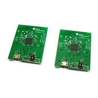
Evaluation Module Kit
Brand: Texas Instruments
|
Category: Motherboard
|
Size: 1 MB
Table of Contents
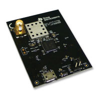
Texas Instruments CC2538 Quick Start Manual (3 pages)
Evaluation Module Kit
Brand: Texas Instruments
|
Category: Motherboard
|
Size: 0 MB
Advertisement
Advertisement
Related Products
- Texas Instruments CD4066BC
- Texas Instruments CD4066BM
- Texas Instruments CC253x
- Texas Instruments CC2530 ZigBee Development Kit
- Texas Instruments CC2533F64
- Texas Instruments CC2533F128
- Texas Instruments CC2533DK-RF4CE-BA
- Texas Instruments HPL-D SLLU064A
- Texas Instruments SN65LVDS125A
- Texas Instruments SN65LVDS250