Sign In
Upload
Manuals
Brands
Schweitzer Engineering Laboratories Manuals
Relays
SEL-421-4
Schweitzer Engineering Laboratories SEL-421-4 Manuals
Manuals and User Guides for Schweitzer Engineering Laboratories SEL-421-4. We have
1
Schweitzer Engineering Laboratories SEL-421-4 manual available for free PDF download: Instruction Manual
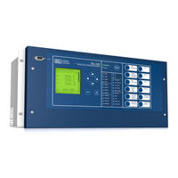
Schweitzer Engineering Laboratories SEL-421-4 Instruction Manual (1518 pages)
Protection, Automation, and Control System
Brand:
Schweitzer Engineering Laboratories
| Category:
Relays
| Size: 30 MB
Table of Contents
Table of Contents
3
Firmware
13
Metering
16
Features
21
Circuit Breaker Monitor
23
Applications
27
Sel Boot
28
Table 8.21 DNP
31
Models and Options
31
Figure 1.1 SEL-421 Functional Overview
32
Specifications
33
Figure 1.3 Single Circuit Breaker Configuration (ESS := 1)
38
Figure 1.5 Double Circuit Breaker Configuration (ESS := 3)
39
Figure 1.4 Single Circuit Breaker Configuration with Line Breaker Cts (ESS := 2)
39
Figure 1.6 Double Circuit Breaker Configuration with Bus Protection (ESS := 4)
40
Figure 1.7 Tapped Line (ESS
40
Table 1.1 Application Highlights
41
Table 1.2 SEL-421 Relay Characteristics
43
Station DC Battery System Monitor
49
Shared Configuration Attributes
51
Figure 2.1 Horizontal Front-Panel Template (A); Vertical Front-Panel Template
53
Figure 2.2 Rear 3U Template, Fixed Terminal Block Analog Inputs
54
Figure 2.3 Rear 3U Template, Connectorized Analog Inputs
55
Table 2.1 Recommended Control Input Pickup Settings
56
Table 2.2 Required Settings for Use with AC Control Signals
57
Figure 2.4 Standard Control Output Connection
58
Figure 2.5 Hybrid Control Output Connection
59
Figure 2.6 High-Speed, High-Current Interrupting Control Output Connection, INT5 (INT8)
60
Figure 2.7 High-Speed, High-Current Interrupting Control Output Connection, INT4
60
Figure 2.8 High-Speed, High-Current Interrupting Control Output Typical Terminals, INT5 (INT8)
61
Figure 2.9 Precharging Internal Capacitance of High-Speed, High-Current Interrupting Output
61
Figure 2.10 INT1 I/O Interface Board
63
Figure 2.11 INT2 I/O Interface Board
63
Figure 2.12 INT3 I/O Interface Board
63
Plug-In Boards
63
Figure 2.17 INT8 I/O Interface Board
64
Figure 2.16 INT7 I/O Interface Board
64
Figure 2.15 INT6 I/O Interface Board
64
Figure 2.14 INT5 I/O Interface Board
64
Figure 2.13 INT4 I/O Interface Board
64
Table 2.3 Control Inputs
65
Table 2.4 Control Outputs
65
Jumpers
65
Table 2.5 Main Board Jumpers
66
Figure 2.18 Jumper Location on the Main Board
66
Figure 2.19 Major Component Locations on the SEL-421 Main Board
68
Table 2.6 Main Board Jumpers-JMP2, JMP3, and JMP4
69
Figure 2.20 Major Component Locations on the SEL-421 INT1, INT2, INT4, INT5, INT6, INT7, and INT8 I/O Boards
71
Figure 2.21 Major Component Locations on the SEL-421 INT3 I/O Board
72
Table 2.9 Jumper Positions for Arc Suppression
73
Table 2.8 Jumper Positions for Breaker OPEN/CLOSE Indication
73
Table 2.7 I/O Board Jumpers
73
Table 2.10 Front-Panel LED Option
74
Relay Placement
74
Figure 2.22 SEL-421 Chassis Dimensions
75
Connection
75
Figure 2.23 3U Rear Panel, Main Board
76
Figure 2.24 3U Rear Panel, Main Board, Connectorized
76
Figure 2.25 Ethercat Board for Tidl
77
Figure 2.26 4U Rear Panel, Main Board, Without Optional I
77
Figure 2.27 4U Rear Panel, Main Board, INT5 I/O Interface Board
77
Figure 2.28 4U Rear Panel, Main Board, INT8 I/O Interface Board
78
Figure 2.29 5U Rear Panel, Main Board, INT3 and INT1 I/O Interface Board
78
Figure 2.30 5U Rear Panel, Main Board, INT4 and INT1 I/O Interface Board
79
Figure 2.31 5U Rear Panel, Main Board, INT6 and INT4 I/O Interface Board
79
Figure 2.32 5U Rear Panel, Main Board, INT2 and INT7 I/O Interface Board
80
Figure 2.33 Rear-Panel Symbols
80
Figure 2.34 Screw-Terminal Connector Keying
81
Figure 2.35 Rear-Panel Receptacle Keying
82
Figure 2.36 Power Connection Area of the Rear Panel
83
Table 2.11 Fuse Requirements for the Power Supply
84
Figure 2.37 Control Output OUT108
86
Figure 2.38 Axion Chassis
88
Figure 2.39 SEL-2243 Power Coupler
89
Figure 2.40 SEL-2244-2 Digital Input Module
90
Figure 2.41 SEL-2244-5 Fast High-Current Digital Output Module
91
Figure 2.42 SEL-2245-42 AC Analog Input Module
92
Figure 2.43 Topology 1
93
Figure 2.44 Topology 2
93
Figure 2.45 Topology 3
94
Table 2.12 Tidl LED Status
95
Figure 2.46 Remote Module Interface
95
Figure 2.47 SEL-421 to Computer-D-Subminiature 9-Pin Connector
97
Figure 2.48 Example Ethernet Panel with Fiber-Optic Ports
98
Figure 2.54 100BASE-FX and 10/100BASE-T Port Configuration on Ports 5C and 5D
99
Figure 2.53 Two 10/100BASE-T Port Configuration on Ports 5C and 5D
99
Figure 2.52 Two 100BASE-FX Port Configuration on Ports 5C and 5D
99
Figure 2.51 100BASE-FX and 10/100BASE-T Port Configuration on Ports 5A and 5B
99
Figure 2.50 Two 10/100BASE-T Port Configuration on Ports 5A and 5B
99
Figure 2.49 Two 100BASE-FX Port Configuration on Ports 5A and 5B
99
AC/DC Connection Diagrams
100
Figure 2.55 Typical External AC/DC Connections-Single Circuit Breaker
101
Figure 2.56 Typical External AC/DC Connections-Dual Circuit Breaker
102
Figure 2.57 SEL-421 Example Wiring Diagram Using the Auxiliary TRIP/CLOSE Pushbuttons
103
Low-Level Test Interface
105
Table 3.1 UUT Database Entries for SEL-5401 Relay Test System Software-5 a Relay
106
Table 3.2 UUT Database Entries for SEL-5401 Relay Test System Software-1 a Relay
106
Figure 3.1 Low-Level Test Interface
106
Relay Test Connections
107
Figure 3.2 Test Connections Using Three Voltage and Three Current Sources
108
Figure 3.3 Test Connections Using Two Current Sources for Phase-To-Phase, Phase-To-Ground, and Two-Phase-To-Ground Faults
109
Figure 3.4 Test Connections Using Two Current Sources for Three-Phase Faults
110
Figure 3.5 Test Connections Using a Single Current Source for a Phase-To-Ground Fault
111
Figure 3.6 Test Connections Using a Single Current Source for a Phase-To-Phase Fault
112
Checking Relay Operation
112
Figure 3.7 Negative-Sequence Instantaneous Overcurrent Element Settings: Quickset
114
Figure 3.8 Uploading Group 1 Settings to the SEL-421
115
Figure 3.9 ELEMENT SEARCH Screen
115
Figure 3.10 RELAY ELEMENTS Screen Containing Element 50Q1
116
Figure 3.11 Group 1 Relay Configuration Settings: Quickset
118
Figure 3.12 Breaker 1 Breaker Monitor Settings: Quickset
119
Figure 3.13 Group 1 Line Configuration Settings: Quickset
120
Table 3.3 Negative-Sequence Directional Element Settings AUTO Calculations
121
Figure 3.14 Directional Settings: Quickset
121
Figure 3.15 Uploading Group 1 and Breaker Monitor Settings to the SEL-421
122
Figure 3.16 RELAY ELEMENTS LCD Screen Containing Elements F32Q and R32Q
122
Figure 3.17 Finding Phase-To-Phase Test Quantities
124
Figure 3.18 Phase-Distance Elements Settings: Quickset
125
Figure 3.19 RELAY ELEMENTS LCD Screen Containing Element MBC2
126
Technical Support
127
Front-Panel LCD Default Displays
129
Table 4.1 Metering Screens Enable Settings
130
Figure 4.1 Sample ROTATING DISPLAY
131
Front-Panel Menus and Screens
131
Target Leds
137
Table 4.2 Front-Panel Target Leds
138
Figure 4.9 Factory-Default Front-Panel Target Areas (16 or 24 Leds)
138
Table 4.3 TIME Target LED Trigger Elements-Factory Defaults
139
Table 4.4 Operator Control Pushbuttons and Leds-Factory Defaults
141
Figure 4.10 Operator Control Pushbuttons and Leds (8 or 12 Pushbuttons)
141
Front-Panel Operator Control Pushbuttons
141
Figure 4.11 Factory-Default Operator Control Pushbuttons
143
One-Line Diagrams
143
Figure 4.12 Bay Control Screen Selected for Rotating Display
144
Figure 4.13 Configuring PB1_HMI for Direct Bay Control Access
145
Figure 4.14 Pole Discrepancy
146
Figure 4.15 Bay with Ground Switch (Option 1)
147
Figure 4.16 Bay Without Ground Switch (Option 2)
147
Figure 4.17 Tie Breaker Bay (Option 3)
148
Figure 4.18 Bay with Ground Switch (Option 4)
148
Figure 4.19 Bay Without Ground Switch (Option 5)
149
Figure 4.20 Transfer Bay (Option 6)
149
Figure 4.21 Tie Breaker Bay (Option 7)
150
Figure 4.22 Bay with Ground Switch (Option 8)
150
Figure 4.23 Bay Without Ground Switch (Option 9)
151
Figure 4.24 Bay with Ground Switch (Option 10)
151
Figure 4.25 Bay Without Ground Switch (Option 11)
152
Figure 4.26 Left Breaker Bay with Ground Switch (Option 12)
152
Figure 4.28 Middle Breaker Bay (Option 14)
153
Figure 4.27 Right Breaker Bay with Ground Switch (Option 13)
153
Figure 4.29 Left Breaker Bay Without Ground Switch (Option 15)
154
Figure 4.30 Right Breaker Bay Without Ground Switch (Option 16)
154
Figure 4.31 Bay with Ground Switch (Option 17)
155
Figure 4.32 Bay Without Ground Switch (Option 18)
155
Figure 4.33 Left Breaker Bay with Ground Switch (Option 19)
156
Figure 4.34 Left Breaker Bay Without Ground Switch (Option 20)
156
Figure 4.35 Right Breaker Bay with Ground Switch (Option 21)
157
Figure 4.36 Right Breaker Bay Without Ground Switch (Option 22)
157
Figure 4.37 Source Transfer (Option 23)
158
Figure 4.38 Throw-Over Bus Type 1 Switch (Option 24)
158
Figure 4.39 Throw-Over Bus Type 2 Switch (Option 25)
159
Figure 4.40 Screen 1
159
Figure 4.41 Screen 2
160
Figure 5.1 Current and Voltage Source Connections for the SEL-421 Relay
162
Figure 5.2 Main and Alternate Line-Current Source Assignments
163
Figure 5.3 Combined Currents for Line-Current Source Assignment
163
Figure 5.4 Breaker Current Source Assignments
163
Table 5.1 Available Current Source Selection Settings Combinations
164
Table 5.2 Available Current Source Selection Settings Combinations When ESS := Y, NUMBK := 1
164
Table 5.3 Available Current Source Selection Settings Combinations When ESS := Y, NUMBK := 2
165
Table 5.4 Available Voltage Source Selection Setting Combinations
166
Figure 5.5 ESS := 1, Single Circuit Breaker Configuration
168
Table 5.6 ESS := 1, Current and Voltage Source Selection
168
Table 5.5 ESS := N, Current and Voltage Source Selection
168
Table 5.7 ESS := 2, Current and Voltage Source Selection
169
Figure 5.6 ESS := 2, Single Circuit Breaker Configuration
169
Table 5.8 ESS := 3, Current and Voltage Source Selection
170
Figure 5.7 ESS := 3, Double Circuit Breaker Configuration
170
Table 5.9 ESS := 4, Current and Voltage Source Selection
171
Figure 5.8 ESS := 4, Double Circuit Breaker Configuration
171
Figure 5.9 Tapped EHV Overhead Transmission Line
172
Figure 5.10 ESS := Y, Tapped Line
172
Table 5.10 ESS := Y, Tapped Line
173
Table 5.11 ESS := Y, Current Polarizing Source
173
Figure 5.11 ESS := Y, Single Circuit Breaker with Current Polarizing Source Tapped Power Transformer
173
Polarizing Quantity for Distance Element Calculations
174
Table 5.12 VMEMC Relay Setting
175
Frequency Estimation
175
Table 5.13 Frequency Measurement and Frequency Tracking Ranges
176
Table 5.14 Frequency Estimation
176
Figure 5.12 SEL-421 Alpha Quantity Calculation
176
Table 5.15 Voltage and Breaker Pole Correlation
177
Table 5.16 Frequency Estimation Outputs
177
Undervoltage Supervision Logic
177
Figure 5.13 Undervoltage Supervision Logic
178
Table 5.17 Table Y12. Summary of the Valpha and 81UVSP Calculations
179
Over- and Underfrequency Elements
179
Figure 5.14 Frequency Element Logic
180
Table 5.18 Time-Error Calculation Inputs and Outputs
181
Figure 5.15 Sample TEC Command Response
182
Figure 5.16 Sample TEC N Command Response
182
Table 5.19 Fault Location Triggering Elements
183
Table 5.20 Fault Type
184
Table 5.21 Fault Location Settings
184
Table 5.22 Fault Location Relay Word Bit
184
Open-Phase Detection Logic
184
Table 5.23 Open-Phase Detection Relay Word Bits
185
Table 5.24 Pole-Open Logic Settings
185
Table 5.25 EPO Setting Selections
185
Table 5.26 Pole-Open Logic Relay Word Bits
185
Figure 5.17 Pole-Open Logic Diagram
187
Loss-Of-Potential Logic
188
Table 5.27 LOP Logic Setting
189
Table 5.28 LOP Logic Relay Word Bits
189
Figure 5.18 LOP Logic Process Overview
190
Figure 5.19 LOP Logic
192
Table 5.29 Fault Type Identification Logic Settings
193
Table 5.30 FIDS Relay Word Bits
193
Table 5.31 Directional Elements Supervising Ground Elements
193
Table 5.32 Ground Directional Element Settings
194
Table 5.33 Ground Directional Element Settings AUTO Calculations
195
Table 5.34 Ground Directional Element Preferred Settings
195
Table 5.35 Ground Directional Element Enables
197
Figure 5.20 32Q and 32QG Enable Logic Diagram
198
Figure 5.21 32V and 32I Enable Logic Diagram
198
Table 5.36 Ground Directional Element Relay Word Bits
199
Figure 5.22 Best Choice Ground Directional Element Logic
200
Figure 5.23 Negative-Sequence Voltage-Polarized Directional Element Logic
201
Figure 5.24 Zero-Sequence Voltage-Polarized Directional Element Logic
201
Figure 5.25 Zero-Sequence Current-Polarized Directional Element Logic
202
Figure 5.26 Ground Directional Element Output Logic Diagram
202
Table 5.39 Phase and Negative-Sequence Directional Elements Relay Word Bits
205
Figure 5.27 32P, Phase Directional Element Logic Diagram
206
Figure 5.28 32Q, Negative-Sequence Directional Element Logic Diagram
206
Directionality
206
Table 5.40 Zone Directional Settings
207
Table 5.41 CVT Transient Detection Logic Setting
207
Table 5.42 CVT Transient Detection Logic Relay Word Bit
208
Figure 5.29 CVT Transient Detection Logic
208
Series-Compensation Line Logic
208
Table 5.43 Series-Compensation Line Logic Relay Settings
209
Figure 5.30 Load-Encroachment Logic Diagram
209
Table 5.44 Load-Encroachment Logic Relay Settings
210
Table 5.45 Load-Encroachment Logic Relay Word Bits
210
Figure 5.31 Load-Encroachment Characteristics
210
Out-Of-Step Logic (Conventional)
210
Figure 5.32 OOS Characteristics
211
Table 5.46 OOS Logic Relay Settings
212
Table 5.47 OOS Logic Relay Word Bits
213
Figure 5.33 OOS Positive-Sequence Measurements
214
Figure 5.34 OOS Override Logic
214
Figure 5.35 OOS Logic Diagram
215
Figure 5.36 Open-Pole OSB Unblock Logic
216
Figure 5.37 Zero-Setting OOS Blocking Function
216
Out-Of-Step Logic (Zero Settings)
216
Figure 5.38 Swing Center Voltage Slope Detection Logic
218
Figure 5.39 Starter Zone Characteristic
219
Figure 5.40 Swing Signature Detector Logic
220
Figure 5.41 Swing Signature Detector Logic
221
Figure 5.42 Reset Conditions Logic
222
Figure 5.43 Type of Power Swings Detected by the DOSB Function
223
Figure 5.44 Dependable Power-Swing Block Detector Logic (EOOS = Y1)
224
Figure 5.45 Dependable Power-Swing Block Detector Logic (EOOS
225
Figure 5.46 Relay Word Bit DOSB Is the or Combination of DOSBY1 and DOSBY
225
Figure 5.47 Logic Diagram of the Three-Phase Fault Detector
226
Figure 5.48 Pole-Open OOS Blocking Logic
226
Table 5.48 Input/Output Combinations of the Pole-Open OOS Blocking Logic
227
Figure 5.49 I0/IA2 Angle Supervision During Pole-Open Situation
227
Figure 5.50 Blocking of the MAG Signal by the OSBA Fault Detection
227
Figure 5.51 Unblocking of the MAB Signal by the 67QUB Element
228
Figure 5.52 Directional Element Signals 67QUBF and 67QUBR
228
Figure 5.53 OST Scheme Logic Resistive and Reactive Blinders
229
Figure 5.54 Logic that Determines Positive-Sequence Impedance Trajectory (EOOS = Y1)
230
Figure 5.55 Out-Of-Step Trip Logic (EOOS = Y1)
231
Figure 5.56 Out-Of-Step Blocking for Zone 1 through Zone 5
232
Mho Ground-Distance Elements
232
Table 5.49 Mho Ground-Distance Elements Relay Word Bits
233
Figure 5.57 Zone 1 Mho Ground-Distance Element Logic Diagram
234
Figure 5.58 Zone 2 Mho Ground-Distance Element Logic Diagram
235
Figure 5.59 Zones 3, 4, and 5 Mho Ground-Distance Element Logic Diagram
236
Quadrilateral Ground-Distance Elements
236
Table 5.50 Differences between the Adaptive Right Resistance Blinder and the Existing Resistance
237
Table 5.51 Quadrilateral Ground-Distance Elements Relay Word Bits
237
Figure 5.60 Zone 1 Quadrilateral Ground-Distance Element Logic Diagram
238
Figure 5.61 Zone 2 Quadrilateral Distance Element Logic Diagram
239
Figure 5.62 Zones 3, 4, and 5 Quadrilateral Ground-Distance Element Logic
240
Mho Phase-Distance Elements
240
Table 5.52 Mho Phase-Distance Elements Relay Word Bits
241
Figure 5.63 Zone 1 Mho Phase-Distance Element Logic Diagram
242
Figure 5.64 Zone 2 Mho Phase-Distance Element Logic Diagram
243
Figure 5.65 Zones 3, 4, and 5 Mho Phase-Distance Element Logic Diagram
244
Table 5.53 High-Speed and Conventional Element Directional Setting Summary
245
Quadrilateral Phase-Distance Elements
245
Figure 5.66 Quadrilateral Phase-Distance Element Characteristic (TANGP = 0)
246
Figure 5.67 Quadrilateral Phase-Distance Element Characteristic (TANGP = -10 Degrees)
247
Figure 5.68 Network to Determine Homogeneity
247
Figure 5.69 Tilt in Apparent Fault Impedance Resulting from Nonhomogeneity
248
Table 5.54 Quadrilateral Phase-Distance Elements Relay Word Bits
249
Figure 5.70 Zone 1 AB Loop Conventional Quadrilateral Phase-Distance Element Logic
250
Figure 5.71 Zone 2 AB Loop Conventional Quadrilateral Phase-Distance Element Logic
250
Figure 5.72 Zone 3, 4, and 5 AB Loop Conventional Quadrilateral Phase-Distance Element Logic
251
Zone Time Delay
251
Figure 5.73 Zone Timers
253
Instantaneous Line Overcurrent Elements
253
Table 5.55 Phase Overcurrent Element Settings
254
Table 5.56 Negative-Sequence Overcurrent Element Settings
254
Table 5.59 Negative-Sequence Instantaneous/Definite-Time Line Overcurrent Relay Word Bits
255
Table 5.58 Phase Instantaneous/Definite-Time Line Overcurrent Relay Word Bits
255
Table 5.57 Residual Ground Overcurrent Element Settings
255
Table 5.60 Residual Ground Instantaneous/Definite-Time Line Overcurrent Relay Word Bits
256
Figure 5.74 Phase Instantaneous/Definite-Time Overcurrent Elements
257
Figure 5.75 Residual Ground Instantaneous/Directional Overcurrent Elements
258
Figure 5.76 Negative-Sequence Instantaneous/Directional Overcurrent Elements
259
Inverse-Time Overcurrent Elements
259
Table 5.61 Selectable Current Quantities
260
Table 5.62 Selectable Inverse-Time Overcurrent Settings
260
Table 5.63 Selectable Inverse-Time Overcurrent Relay Word Bits
261
Table 5.64 Equations Associated with U.S. Curves
261
Table 5.65 Equations Associated with IEC Curves
262
Figure 5.77 U.S. Moderately Inverse-U1
263
Figure 5.78 U.S. Inverse-U2
264
Figure 5.79 U.S. very Inverse-U3
265
Figure 5.80 U.S. Extremely Inverse-U4
266
Figure 5.81 U.S. Short-Time Inverse-U5
267
Figure 5.82 IEC Standard Inverse-C1
268
Figure 5.83 IEC very Inverse-C2
269
Figure 5.84 IEC Extremely Inverse-C3
270
Figure 5.85 IEC Long-Time Inverse-C4
271
Figure 5.86 IEC Short-Time Inverse-C5
272
Figure 5.87 Selectable Inverse-Time Overcurrent Element Logic Diagram
273
Figure 5.88 Undervoltage Elements
273
Over- and Undervoltage Elements
273
Table 5.66 Available Input Quantities
274
Figure 5.89 Overvoltage Elements
274
Switch-Onto-Fault Logic
277
Table 5.67 SOTF Settings
278
Table 5.68 SOTF Relay Word Bits
278
Figure 5.90 SOTF Logic Diagram
279
Table 5.69 ECOMM Setting
280
Figure 5.91 Required Zone Directional Settings
280
Communications-Assisted Tripping Logic
280
Directional Comparison Blocking Scheme
281
Table 5.70 DCB Settings
283
Table 5.71 DCB Relay Word Bits
283
Permissive Overreaching Transfer Tripping Scheme
284
Figure 5.92 DCB Logic Diagram
284
Table 5.72 POTT Settings
287
Table 5.73 POTT Relay Word Bits
288
Figure 5.93 Permissive Trip Receiver Logic Diagram
289
Figure 5.94 POTT Logic Diagram
290
Figure 5.95 POTT Cross-Country Logic Diagram
291
Figure 5.96 POTT Scheme Logic (ECOMM := POTT3) with Echo and Weak Infeed
292
Directional Comparison Unblocking Scheme Logic
293
Table 5.74 DCUB Settings
294
Table 5.75 DCUB Relay Word Bits
295
Figure 5.97 Permissive Trip Received Logic Diagram
295
Figure 5.98 DCUB Logic Diagram
296
Table 5.76 Additional Settings for Single Pole Tripping (SPT)
297
Trip Logic
297
Table 5.77 Setting TULO Unlatch Trip Options
299
Table 5.78 Trip Logic Settings
300
Figure 5.99 Trip Logic Diagram
302
Table 5.79 Trip Logic Relay Word Bits
304
Figure 5.100 Two Circuit Breakers Trip Logic Diagram
305
Figure 5.101 Trip a Unlatch Logic
306
Figure 5.102 Trip During Open Pole
306
Circuit Breaker Failure Protection
306
Figure 5.103 Scheme 1 Logic Diagram
307
Figure 5.104 Scheme Y1 Circuit Breaker Failure Logic
308
Figure 5.105 Scheme 2 Three-Pole Circuit Breaker Failure Protection Logic
309
Figure 5.106 Scheme Y2 Three-Pole Circuit Breaker Failure Logic
309
Figure 5.107 Scheme 2 Single-Pole Circuit Breaker Failure Protection Logic
310
Figure 5.108 Scheme Y2 Single-Pole Circuit Breaker Failure Protection Logic
310
Figure 5.109 Scheme 2 Current-Supervised Three-Pole Retrip Logic
311
Figure 5.110 Scheme Y2 Current-Supervised Three-Pole Retrip Logic
311
Figure 5.111 Scheme 2 Current-Supervised Single-Pole Retrip Logic
311
Figure 5.112 Scheme Y2 Current-Supervised Single-Pole Retrip Logic
312
Figure 5.113 no Current/Residual Current Circuit Breaker Failure Protection Logic Diagram
312
Table 5.80 Circuit Breaker Failure Relay Word Bits
315
Figure 5.114 Circuit Breaker Failure Seal-In Logic Diagram
316
Figure 5.117 Circuit Breaker Failure Trip Logic Diagram
317
Figure 5.116 Flashover Protection Logic Diagram
317
Figure 5.115 Failure to Interrupt Load Current Logic Diagram
317
Figure 5.118 Partial Breaker-And-A-Half or Partial Ring-Bus Breaker Arrangement
318
Synchronism Check
318
Figure 5.119 Synchronism-Check Voltages for Two Circuit Breakers
319
Figure 5.120 Synchronism-Check Settings
320
Table 5.81 Synchronism-Check Relay Word Bits
321
Figure 5.121 Synchronism-Check Relay Word Bits
321
Figure 5.122 Example Synchronism-Check Voltage Connections to the SEL-421
323
Figure 5.123 Synchronism-Check Voltage Reference
324
Figure 5.124 Normalized Synchronism-Check Voltage Sources VS1 and VS2
325
Figure 5.125 Healthy Voltage Window and Indication
326
Figure 5.126 Synchronism-Check Voltage Difference Logic
326
Figure 5.127 Synchronism-Check Enable Logic
328
Figure 5.128 "No Slip" System Synchronism-Check Element Output Response
330
Figure 5.129 "Slip-No Compensation" Synchronism-Check Element Output Response
331
Figure 5.130 "Slip-With Compensation" Synchronism-Check Element Output Response
333
Figure 5.131 Alternative Synchronism-Check Source 2 Example and Settings
335
Figure 6.1 230 Kv Overhead Transmission Line
337
Kv Overhead Distribution Line Example
337
Table 6.1 System Data-230 Kv Overhead Transmission Line
338
Table 6.2 Secondary Impedances
338
Figure 6.2 Circuit Breaker Arrangement at Station
339
Table 6.3 LOP Enable Options
342
Table 6.4 Options for Enabling Pole-Open Logic
348
Table 6.5 Setting TULO Unlatch Trip Options
350
Table 6.6 Settings for 230 Kv Overhead TX Example
351
Kv Parallel Transmission Lines with Mutual Coupling Example
354
Table 6.7 System Data-500 Kv Parallel Overhead Transmission Lines
355
Figure 6.3 500 Kv Parallel Overhead Transmission Lines
355
Table 6.8 Secondary Impedances
356
Figure 6.4 Circuit Breaker-And-A-Half Arrangement: Station S, Line 1
358
Table 6.9 LOP Enable Options
361
Figure 6.5 Quadrilateral Ground-Distance Element Reactive Reach Setting
364
Figure 6.6 Definition of Homogeneous Network
366
Table 6.10 Tilt Resulting from Nonhomogeneity
367
Figure 6.7 Tilt in Apparent Fault Impedance Resulting from Nonhomogeneity
367
Figure 6.8 Nonhomogeneous Angle Setting
368
Table 6.11 Options for Enabling Pole-Open Logic
373
Table 6.12 Trip Unlatch Options
378
Figure 6.9 Current Distribution During Cross-Country Fault
380
Figure 6.10 Simplified POTT Scheme KEY1/KEY3 Logic
381
Table 6.13 Settings for 500 Kv Parallel TX Example
383
Kv Tapped Overhead Transmission Line Example
389
Table 6.14 System Data-345 Kv Tapped Overhead Transmission Line
390
Figure 6.11 345 Kv Tapped Overhead Transmission Line
390
Table 6.15 Secondary Impedances
391
Figure 6.12 Circuit Breaker Arrangement at Station
393
Table 6.16 LOP Enable Options
396
Table 6.17 Local Zone 2 Fault Impedance Measurements
398
Figure 6.13 Reverse Zone 3 Coordination
398
Table 6.18 Apparent Impedance Measurement for Remote Faults
399
Figure 6.14 Impedance Diagram
399
Figure 6.15 Load-Encroachment Function
403
Figure 6.16 345 Kv Tapped Line Negative-Sequence Network
409
Figure 6.17 345 Kv Tapped Line Zero-Sequence Network
411
Table 6.19 Options for Enabling Pole-Open Logic
413
Figure 6.18 DC Schematic for DCB Trip Scheme
416
Table 6.20 Setting TULO Unlatch Trip Options
417
Table 6.21 Settings for 345 Kv Tapped TX Example
419
EHV Parallel 230 Kv Underground Cables Example
423
Figure 6.19 230 Kv Parallel Underground Cables
423
Table 6.22 System Data-230 Kv Parallel Underground Cables
423
Table 6.23 Secondary Impedances
424
Figure 6.20 Circuit Breaker Arrangement at Station S, Cable 1
426
Table 6.24 LOP Enable Options
429
Figure 6.21 Quadrilateral Ground-Distance Element Reactive Reach Setting
431
Figure 6.22 Circuit to Determine Network Homogeneity
433
Table 6.25 Tilt Resulting from Nonhomogeneity
434
Figure 6.23 Apparent Fault Impedance Resulting from Nonhomogeneity
434
Figure 6.24 Nonhomogeneous Angle Setting
435
Table 6.26 XAG Measurement for Remote AG Fault
437
Figure 6.25 External Ground Fault
438
Figure 6.26 Negative-Sequence Fault Current Distribution-External Ground Fault
441
Figure 6.27 Reverse Unbalanced Fault on Cable Circuit (Shunt Admittance)
445
Table 6.29 Options for Enabling Pole-Open Logic
446
Table 6.30 Setting TULO Unlatch Trip Options
449
Table 6.31 Settings for 230 Kv Parallel Cables Example
451
Figure 6.28 500 Kv Power System
455
Out-Of-Step Logic Application Examples
455
Table 6.32 Positive-Sequence Impedances (Secondary)
456
Figure 6.29 OOS Characteristic Settings Parameters
457
Figure 6.30 Calculating Setting R1R7
459
Figure 6.31 Swing Trajectory to Determine the OSBD Setting
461
Figure 6.32 Inner Blinders
463
Table 6.33 Automatically Calculated/Hidden Settings
465
Table 6.34 Relay Configuration (Group)
465
Table 6.35 Out-Of-Step Tripping/Blocking
466
Figure 6.33 OST Characteristics
467
Table 6.36 Automatically Calculated/Hidden Settings
472
Table 6.37 Relay Configuration (Group)
472
Table 6.38 Out-Of-Step Tripping/Blocking
472
Figure 6.34 230 Kv Example Power System
473
Autoreclose Example
473
Figure 6.35 Circuit Breaker Arrangement at Station
474
Table 6.39 Settings for Autoreclose Example
476
Figure 6.36 Potential Sources
476
Autoreclose and Synchronism-Check Example
477
Figure 6.37 500 Kv Power System
477
Figure 6.38 Partial Circuit Breaker-And-A-Half Arrangement at Station S, Line
479
Figure 6.39 Potential Sources
483
Table 6.40 Settings for Autoreclose and Synchronism Check Example
485
Circuit Breaker Failure Application Examples
487
Figure 6.40 Scheme 1 All Faults and Scheme 2 Multiphase Fault Timing Diagram
490
Figure 6.41 Scheme 2 Single-Phase Fault Timing Diagram
491
Figure 6.42 230 Kv Power System for Circuit Breaker Failure Scheme 1
491
Table 6.41 Secondary Quantities
492
Figure 6.43 Timing Diagram for Setting BFPU1-Scheme 1
493
Table 6.42 Settings for Circuit Breaker Failure Example
496
Figure 6.44 Circuit Breaker Failure Trip and Circuit Breaker Trip DC Connections
496
Figure 6.45 500 Kv Power System for Circuit Breaker Failure Scheme 2
498
Table 6.43 Secondary Quantities
498
Figure 6.46 Fault Current Distribution through Faulted Line at Station
499
Figure 6.47 Timing Diagram for Setting BFPU1-Scheme 2
500
Figure 6.48 Timing Sequences for Circuit Breaker Failure Protection Scheme 2
501
Table 6.44 Settings for Circuit Breaker Failure Example
504
Figure 6.49 Circuit Breaker BK1 DC Connections (Two Trip Coils)
504
Figure 6.50 230 Kv Tapped Overhead Transmission Line
506
Kv Tapped Transmission Line Application Example
506
Figure 6.51 Automatic Restoration Timing Diagram
507
Figure 6.52 SEL-421 Inputs
509
Table 6.45 Global Settings
510
Table 6.46 Breaker Monitor Settings
510
Table 6.47 Group Settings
511
Figure 6.53 Protection Free-Form SEL OGIC Control Equations
514
Table 6.49 Control Inputs
515
Table 6.50 Control Outputs (SEL OGIC Control Equations)
515
Figure 6.54 Protection Freeform SEL OGIC Control Equations
517
Table 7.1 MET Command
522
Table 7.2 Instantaneous Metering Quantities-Voltages, Currents, Frequency
523
Table 7.3 Instantaneous Metering Quantities-Power
524
Figure 7.1 Complex Power (P/Q) Plane
524
Table 7.4 Maximum/Minimum Metering Quantities-Voltages, Currents, Frequency, and Powers
525
Table 7.5 Demand and Peak Demand Metering Quantities-LINE
526
Table 7.6 Energy Metering Quantities-(LINE)
526
Table 7.7 Event Report Nonvolatile Storage Capability When ERDIG
528
Table 7.8 Event Report Nonvolatile Storage Capability When ERDIG
528
Figure 7.2 Fixed Analog Section of the Event Report
529
Table 7.9 Event Report Metered Analog Quantities
530
Figure 7.3 Digital Section of the Event Report
531
Figure 7.4 Sample Digital Portion of the Event Report
532
Figure 7.5 Summary Section of the Event Report
533
Figure 7.6 Sample Event Summary Report
533
Table 7.10 Event Types
534
Figure 7.7 Sample Event History
535
Table 8.1 Global Settings Changes
537
Alias Settings
537
Table 8.4 Global Enables
538
Table 8.2 Global Settings Categories
538
Table 8.3 General Global Settings
538
Table 8.5 Station DC1 Monitor (and Station DC2 Monitor)
539
Table 8.6 Control Inputs
539
Table 8.7 Main Board Control Inputs
539
Table 8.8 Interface Board #1 Control Inputs
540
Table 8.9 Interface Board #2 Control Inputs
540
Table 8.10 Settings Group Selection
541
Table 8.11 Frequency Estimation
541
Table 8.12 Time-Error Calculation
541
Table 8.13 Current and Voltage Source Selection
541
Table 8.15 Phasors Included in the Data
542
Table 8.14 Synchronized Phasor Configuration Settings
542
Table 8.16 Synchronized Phasor Configuration Settings Part 2
543
Table 8.17 Synchronized Phasor Recorder Settings
543
Table 8.18 Synchronized Phasor Real Time Control Settings
544
Table 8.19 Time and Date Management
544
Table 8.20 Data Reset Control
544
Table 8.22 Breaker Monitor Settings Categories
545
Table 8.23 Enables
545
Table 8.24 Breaker 1 Inputs
545
Breaker Monitor Settings
545
Table 8.27 Breaker 1 Contact Wear (and Breaker 2 Contact Wear)
546
Table 8.26 Breaker 1 Monitor (and Breaker 2 Monitor)
546
Table 8.25 Breaker 2 Inputs
546
Table 8.28 Breaker 1 Electrical Operating Time (and Breaker 2 Electrical Operating Time)
547
Table 8.29 Breaker 1 Mechanical Operating Time (and Breaker 2 Mechanical Operating Time)
547
Table 8.30 Breaker 1 Pole Scatter and Pole Discrepancy
547
Table 8.31 Breaker 1 Inactivity Time Elapsed (and Breaker 2 Inactivity Time Elapsed)
547
Table 8.32 Breaker 1 Motor Running Time (and Breaker 2 Motor Running Time)
547
Table 8.33 Breaker 1 Current Interrupted (and Breaker 2 Current Interrupted)
547
Table 8.34 Group Settings Categories
548
Group Settings
548
Table 8.35 Line Configuration
549
Table 8.36 Relay Configuration
549
Table 8.38 Quadrilateral Phase-Distance Element Reach
551
Table 8.37 Mho Phase-Distance Element Reach
551
Table 8.39 Phase-Distance Element Time Delay
552
Table 8.40 Mho Ground-Distance Element Reach
552
Table 8.41 Quad Ground-Distance Element Reach
553
Table 8.42 Zero-Sequence Compensation Factor
554
Table 8.43 Ground-Distance Element Time Delay
554
Table 8.44 Series Compensation
554
Table 8.45 Distance Element Common Time Delay
554
Table 8.46 Switch-Onto-Fault Scheme
555
Table 8.47 Out-Of-Step Tripping/Blocking
555
Table 8.48 Load Encroachment
556
Table 8.51 Phase Instantaneous Definite-Time Overcurrent Torque Control
557
Table 8.50 Phase Definite-Time Overcurrent Time Delay
557
Table 8.49 Phase Instantaneous Overcurrent Pickup
557
Table 8.52 Residual Ground Instantaneous Overcurrent Pickup
558
Table 8.53 Residual Ground Definite-Time Overcurrent Time Delay
558
Table 8.54 Residual Ground Instantaneous Definite-Time Overcurrent Torque Control
558
Table 8.55 Negative-Sequence Instantaneous Overcurrent Pickup
559
Table 8.56 Negative-Sequence Definite-Time Overcurrent Time Delay
559
Table 8.57 Negative-Sequence Instantaneous Definite-Time Overcurrent Torque Control
559
Table 8.58 Selectable Operating Quantity Inverse Time Overcurrent Element 1
559
Table 8.61 81 Elements
561
Table 8.62 under Voltage (27) Element
561
Table 8.63 over Voltage (59) Element
561
Table 8.66 Pole-Open Detection
562
Table 8.65 Directional Control Element
562
Table 8.64 Zone/Level Direction
562
Table 8.67 POTT Trip Scheme
563
Table 8.68 DCUB Trip Scheme
563
Table 8.69 DCB Trip Scheme
564
Table 8.70 Breaker 1 Failure Logic (and Breaker 2 Failure Logic)
564
Table 8.71 Synchronism-Check Element Reference
565
Table 8.72 Breaker 1 Synchronism Check
565
Table 8.73 Breaker 2 Synchronism Check
565
Table 8.74 Recloser and Manual Closing
566
Table 8.75 Single-Pole Reclose Settings
567
Table 8.76 Three-Pole Reclose Settings
567
Table 8.78 Demand Metering
568
Table 8.77 Voltage Elements
568
Table 8.80 Trip Logic
569
Notes Settings
570
Table 8.82 Main Board Default Values
571
Table 8.83 Front-Panel Settings Defaults
571
Output Settings
571
Report Settings
574
Table 8.85 Bay Settings
575
DNP3 Settings—Custom Maps
575
Table 9.1 SEL-421 List of Commands
578
Description of Commands
578
Table 9.2 MET Command
580
Table 9.5 MET SYN Command
581
Table 9.4 MET RMS Command
581
Table 9.3 MET E Command
581
Table 9.6 SET Command Overview
582
Table 9.7 SHO Command Overview
583
Table 10.1 SEL-421 Database Regions
585
Communications Database
585
Table 10.2 SEL-421 Database Structure-LOCAL Region
586
Table 10.3 SEL-421 Database Structure-METER Region
586
Table 10.4 SEL-421 Database Structure-DEMAND Region
588
Table 10.5 SEL-421 Database Structure-TARGET Region
589
Table 10.6 SEL-421 Database Structure-HISTORY Region
589
Table 10.8 SEL-421 Database Structure-STATUS Region
590
Table 10.7 SEL-421 Database Structure-BREAKER Region
590
Table 10.9 SEL-421 Database Structure-ANALOGS Region
591
Figure 10.1 MAP 1:METER Command Example
592
DNP3 Communication
592
Table 10.10 SEL-421 DNP3 Reference Data Map
593
Table 10.11 SEL-421 Object 12 Control Operations
598
Table 10.12 Object 30, 32, FTYPE Upper Byte-Event Cause
600
Table 10.13 Object 30, 32, FTYPE Lower Byte-Affected Phase
600
Table 10.14 SEL-421 DNP3 Default Data Map
600
Table 10.15 Logical Device: PRO (Protection)
606
IEC 61850 Communication
606
Table 10.16 Logical Device: MET (Metering)
611
Synchrophasors
614
Table 10.17 Voltage Synchrophasor Names
614
Table 10.18 Current Synchrophasor Names
614
Table 10.19 Synchrophasor Order in Data Stream (Voltages and Currents)
615
Table 11.1 Alphabetic List of Relay Word Bits
617
Alphabetical List
617
Table 11.2 Relay Word Bits: Enable and Tripping Bits
650
Table 11.3 Relay Word Bits: Distance Elements
650
Row Lists
650
Table 11.4 Relay Word Bits: Series-Compensated Line Logic
653
Table 11.5 Relay Word Bits: Out-Of-Step Elements
654
Table 11.6 Relay Word Bits: Directional Elements
655
Table 11.8 Relay Word Bits: Synchronism-Check Elements
656
Table 11.7 Relay Word Bits: Overcurrent Elements
656
Table 11.9 Relay Word Bits: Reclosing Elements
657
Table 11.10 Relay Word Bits: Miscellaneous Elements
659
Table 11.11 Relay Word Bits: Trip Logic Elements
659
Table 11.12 Relay Word Bits: Pilot Tripping Elements
661
Table 11.13 Relay Word Bits: Future Breaker Open-Phase Detector
662
Table 11.14 Relay Word Bits: Breaker 1 Failure
662
Table 11.15 Relay Word Bits: Breaker 2 Failure
663
Table 11.16 Relay Word Bits: 52 Status and Open-Phase Detector
664
Table 11.17 Relay Word Bits: Breaker Monitoring
666
Table 11.18 Relay Word Bits: RTD Status Bits
666
Table 11.22 Relay Word Bits: Local Bits
667
Table 11.20 Relay Word Bits: Metering Elements
667
Table 11.21 Relay Word Bits: Open and Close
667
Table 11.19 Relay Word Bits: Battery Monitor
667
Table 11.23 Relay Word Bits: Remote Bits
668
Table 11.24 Relay Word Bits: Settings Group Bits
668
Table 11.25 Relay Word Bits: Future Breaker Failure Bits
668
Table 11.26 Relay Word Bits: Input Elements
668
Table 11.34 Relay Word Bits: Automation Sequencing Timers
670
Table 11.37 Relay Word Bits: Alarms
671
Table 11.38 Relay Word Bits: Time and Date Management and Frequency Estimation
671
Table 11.39 Relay Word Bits: Pushbuttons and Outputs
672
Table 11.43 Relay Word Bits: Target Logic Bits
673
Table 11.42 Relay Word Bits: Data Reset Bits
673
Table 11.41 Relay Word Bits: Pushbutton LED Bits
673
Table 11.44 Relay Word Bits: M
674
Table 11.45 Relay Word Bits: Test Bits
674
Table 11.46 Relay Word Bits: Virtual Bits
674
Table 11.47 Relay Word Bits: Ethernet Switch
675
Table 11.48 Relay Word Bits: Signal Profiling
676
Table 11.49 Relay Word Bits: Fast SER Enable Bits
676
Table 11.50 Relay Word Bits: Source Selection Elements
676
Table 11.51 Relay Word Bits: Full-Cycle Mho and Quad Ground-Distance
677
Table 11.52 Relay Word Bits: Full-Cycle Mho and Phase Quad Phase-Distance
677
Table 11.53 Relay Word Bits: High-Speed Mho and Quad Ground-Distance
678
Table 11.54 Relay Word Bits: High-Speed Mho and Quad Phase-Distance
679
Table 11.55 Relay Word Bits: DNP Event Lock
680
Table 11.57 Relay Word Bits: IRIG-B Control
681
Table 11.58 Relay Word Bit: Time-Error Calculation
681
Table 11.59 Relay Word Bits: Synchrophasor Configuration Error
682
Table 11.60 Relay Word Bits: Pushbuttons, Pushbutton Leds, and Target Leds for New HMI
682
Table 11.61 Relay Word Bits: Local Bit Supervision
683
Table 11.62 Relay Word Bits: Local Bit Status
683
Table 11.63 Relay Word Bits: RTC Remote Digital Status
683
Table 11.64 Relay Word Bits: Fast Operate Transmit Bits
683
Table 11.65 Relay Word Bits: Bay Control Disconnect Status
684
Table 11.67 Relay Word Bits: Bay Control Disconnect Control
686
Table 11.66 Relay Word Bits: Bay Control Disconnect Bus-Zone Compliant
686
Table 11.68 Relay Word Bits: Bay Control Disconnect Timers and Breaker Status
688
Table 11.69 Under/Overvoltage Elements
692
Table 11.70 Relay Word Bits: 81 Frequency Elements
693
Table 11.71 Full-Cycle Mho and Quad Distance
694
Table 11.72 Time and Date Management
695
Table 11.73 Remote Axion Status
695
Table 11.74 Additional Inputs and Outputs
695
Table 12.1 Analog Quantities Sorted Alphabetically
697
Table 12.2 Analog Quantities Sorted by Function
708
ICD File
721
Table A.1 Firmware Revision History
722
Table A.2 SEL BOOT Revision History
729
Table A.3 ICD File Revision History
729
Table A.4 Instruction Manual Revision History
730
Table B.1 Relay Word Bit Differences
733
Table B.2 Analog Quantity Differences
734
Analog Quantity Changes
734
Table B.3 Global Settings Differences
735
Table B.4 Group Settings Differences
735
Global Settings Changes
735
Table B.5 Serial Port Settings Differences
736
Table B.6 Ethernet Port Settings Differences
736
Front-Panel Settings Changes
736
Table B.7 Binary Inputs Point Mapping for MAPSEL = B
738
DNP3 Mapping Changes
738
Table B.8 Binary Inputs Point Mapping for MAPSEL = E
739
Table B.9 Binary Outputs Point Mapping
739
Table B.10 Counters Point Mapping
741
Table B.11 Analog Inputs Point Mapping
741
Table B.12 Analog Outputs Point Mapping
745
Table B.13 Binary Outputs Mapping for DNP3 LAN/WAN
746
Table B.14 IEC 61850 Functional Differences
748
Table B.15 Default Dataset Differences
748
Table B.16 Logical Node Mapping Differences
748
IEC 61850 Object Changes
748
Control Equation Programming
759
Section 14: ASCII Command Reference
778
Section 15: Communications Interfaces
778
Serial Communication
821
SEL MIRRORED BITS Communication
1301
SEL Distributed Port Switch Protocol (LMD)
1307
SEL-2600A RTD Module Operation
1309
Direct Networking Example
1310
Section 16: DNP3 Communication Introduction to DNP3
1318
DNP3 in the Relay
1323
DNP3 Documentation
1328
DNP3 Serial Application Example
1342
DNP3 LAN/WAN Application Example
1347
Section 17: IEC 61850 Communication
1351
Introduction to IEC 61850
1352
IEC 61850 Operation
1353
Sampled Values
1365
Simulation Mode
1371
IEC 61850 Configuration
1372
Logical Nodes
1379
Protocol Implementation Conformance Statement
1394
ACSI Conformance Statements
1400
Potential Client and Automation Application Issues with Edition 2 Upgrades
1404
Introduction
1407
Section 18: Synchrophasors
1407
Synchrophasor Measurement
1409
Settings for Synchrophasors
1412
Synchrophasor Quantities
1424
View Synchrophasors by Using the MET PM Command
1427
C37.118 Synchrophasor Protocol
1429
SEL Fast Message Synchrophasor Protocol
1435
Control Capabilities
1439
PMU Recording Capabilities
1448
Section 19: Remote Data Acquisition Time-Domain Link (Tidl)
1452
IEC 61850-9-2 Sampled Values
1455
Appendix A: Manual Versions
1465
Appendix B: Firmware Upgrade Instructions Upgrade Procedure
1472
Time-Domain Link (Tidl) Firmware Upgrade
1483
Troubleshooting
1485
Technical Support
1486
Appendix C: Cybersecurity Features
1487
Ports and Services
1487
Authentication and Authorization Controls
1488
Logging Features
1489
Malware Protection Features
1489
Configuration Control Support
1490
Physical Access Security
1490
Backup and Restore
1491
Decommissioning
1491
Vulnerability Notification Process
1491
Glossary
1493
Advertisement
Advertisement
Related Products
Schweitzer Engineering Laboratories SEL-421-5
Schweitzer Engineering Laboratories SEL-487V
Schweitzer Engineering Laboratories SEL-411L
Schweitzer Engineering Laboratories SEL-487B-2
Schweitzer Engineering Laboratories SEL-311A
Schweitzer Engineering Laboratories SEL-251
Schweitzer Engineering Laboratories SEL-352-2
Schweitzer Engineering Laboratories SEL-311C
Schweitzer Engineering Laboratories SEL-749M
Schweitzer Engineering Laboratories SEL-151C
Schweitzer Engineering Laboratories Categories
Relays
Computer Hardware
Transceiver
Protection Device
Measuring Instruments
More Schweitzer Engineering Laboratories Manuals
Login
Sign In
OR
Sign in with Facebook
Sign in with Google
Upload manual
Upload from disk
Upload from URL