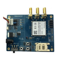
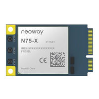
Sign In
Upload
Manuals
Brands
Neoway Manuals
Control Unit
N75
Neoway N75 Manuals
Manuals and User Guides for Neoway N75. We have
3
Neoway N75 manuals available for free PDF download: Hardware User's Manual, Product Specifications
Neoway N75 Hardware User's Manual (95 pages)
Brand:
Neoway
| Category:
Control Unit
| Size: 2 MB
Table of Contents
Table of Contents
3
1 About N75
11
Product Overview
11
Table 1-1 Variant and Frequency Bands
11
Block Diagram
12
Figure 1-1 Block Diagram
12
Basic Features
13
2 Module Pins
15
Pad Layout
15
Figure 2-1 N75 Pin Definition (Top View)
15
Pin Description
16
Table 2-1 IO Types and Level Features
16
Table 2-2 Pin Description
17
3 Application Interfaces
24
Power Interface
24
Vbat
24
Figure 3-1 Current Peaks and Voltage Drops (GSM/GPRS)
25
Figure 3-2 Recommended Design 1
25
Figure 3-3 Recommended Design 2
26
Figure 3-4 Recommended Design 3
27
Figure 3-5 Recommended Design 4
27
Vdd_1P8
28
Control Interfaces
29
Pwrkey_N
29
Figure 3-6 Reference Design of Startup Controlled by Button
29
Table 3-1 VDD_1P8 Electrical Features
29
Figure 3-7 Reference Design of Startup Controlled by MCU
30
Figure 3-8 Reference Design of Automatic Start Once Powered up
30
Reset_N
31
Figure 3-9 N75 On/Off Timing
31
Figure 3-10 Reset Controlled by Button
32
Figure 3-11 Reset Circuit with Triode Separating
32
Figure 3-12 Reset Timing of N75
32
Peripheral Interfaces
33
Usb
33
Table 3-2 Compliant Standards of Peripheral Interfaces
33
Figure 3-13 USB Connection
34
Figure 3-14 Reference Design of USB OTG Function
34
Usim
35
Figure 3-15 Reference Design of USIM Card Interface
36
Uart
37
Figure 3-16 Reference Design of UART Connection (with Flow Control)
37
Figure 3-17 Reference Design of UART Connection (Without Flow Control)
37
Figure 3-18 Recommended Level Shifting Circuit 1
38
Figure 3-19 Recommended Level Shifting Circuit 2
39
Sdc
40
Figure 3-20 Recommended Level Shifting Circuit 3
40
Figure 3-21 SD Connection
41
Table 3-3 SD Card Feature Parameters
41
Figure 3-22 SDC SDR Timing
42
I2S/Pcm
43
Figure 3-23 SDC DDR Timing
43
Table 3-4 Timing Parameters of SDC Interface
43
Figure 3-24 I2S Connection
44
Figure 3-25 I2S Timing
45
Table 3-5 Timing Parameters of I2S Interface
45
Table 3-6 PCM Work Modes
45
Figure 3-26 PCM Connection
46
Figure 3-27 PCM Sync Signal Timing in Primary Mode
46
Figure 3-28 PCM Data Input Timing in Primary Mode
46
Figure 3-29 PCM Data Output Timing in Primary Mode
47
Figure 3-30 PCM Sync Signal Timing in Auxiliary Mode
47
Table 3-7 Parameters of PCM Timing in Primary Mode
47
Figure 3-31 PCM Data Input Timing in Auxiliary Mode
48
Figure 3-32 PCM Data Output Timing in Auxiliary Mode
48
Table 3-8 Parameters of PCM Timing in Auxiliary Mode
48
Spi
49
Figure 3-33 SPI Connection
49
I2C
50
Figure 3-34 SPI Timing
50
Table 3-9 Timing Parameters of SPI Interface
50
Figure 3-35 I2Cconnection
51
Table 3-10 I2C Feature Parameters
51
Figure 3-36 I2C Data Transmission
52
Figure 3-37 I2C Timing
52
Table 3-11 I2C Timing Parameters (Standard Mode)
52
Table 3-12 I2C Timing Parameters (Fast Mode)
53
Table 3-13 I2C Timing Parameters (Fast Mode Plus)
53
Network and Connection
54
Ethernet
54
Figure 3-38 SGMII Connection
55
Figure 3-39 Connection between MDIO and PHY
56
Figure 3-40 MDIO Input Timing
56
Figure 3-41 MDIO Output Timing
56
Wlan
57
Table 3-14 SDIO/WLAN Feature Parameters
57
Figure 3-42 WLAN Connection
58
Figure 3-43 SDIO SDR Timing
59
Figure 3-44 SDIO DDR Timing
59
Table 3-15 Timing Parameters of SDIO/WLAN Interface
59
Bluetooth
60
RF Interface
61
Figure 3-45 Bluetooth Connection
61
ANT_MAIN/ANT_DIV Antenna Interface
62
Figure 3-46 L Network
62
Figure 3-47 Split Capacitor Network
62
Figure 3-48 Pi Network
63
ANT_GNSS Interface
64
Figure 3-49 Recommended RF PCB Design 1
64
Figure 3-50 GNSS RF Structure
64
Figure 3-51 Reference Design of Passive GNSS Antenna
65
Figure 3-52 Reference Design of Active GNSS Antenna
66
Antenna Assembling
67
Figure 3-53 Reference Layout of GNSS Antenna Traces
67
Gpio
68
Figure 3-54 Specifications of MM9329-2700RA1
68
Figure 3-55 RF Connections
68
MUX Interfaces
69
Table 3-16 MUX Pins
69
Other Interfaces
72
Gnss_Lna_En
72
Adc
72
Ring
72
Figure 3-56 Pulse Wave for an Incoming Call
72
Dtr
73
Figure 3-57 RING Indicator for SMS
73
Figure 3-58 Process of Entering Sleep Mode
73
Figure 3-59 Incoming Call Service Process
74
Figure 3-60 Outgoing Call Service Process
74
Figure 3-61 Process of Exiting from Sleep Mode
74
Usb_Boot
75
Figure 3-62 Reference Design of USB_BOOT
75
4 Electric Feature and Reliability
76
Electric Features
76
Table 4-1 Electric Features
76
Table 4-2 Current Consumption of N75
76
Temperature Features
78
Table 4-3 Temperature Features
78
ESD Protection
79
Table 4-4 ESD Protection Features
79
5 RF Features
80
Operating Bands
80
Table 5-1 Operating Bands
80
TX Power and RX Sensitivity
81
Table 5-2 RF TX Power
81
GNSS Feature
82
6 Mechanical Features
84
Dimensions
84
Figure 6-1 N75 Dimensions
84
Label
85
Pack
85
Reel&Tape
85
Figure 6-2 N75 Label
85
Moisture
87
7 Mounting the Module Onto the Application Board
88
Bottom Dimensions
88
Figure 7-1 Bottom View
88
Application Foot Print
89
Stencil
89
Solder Paste
89
Figure 7-2 Recommended Application Foot Print (Top View)
89
SMT Furnace Temperature Curve
90
Figure 7-3 SMT Furnace Temperature Curve
90
8 Safety Recommendations
91
Conformity and Compliance
92
Approvals
92
American Notice
92
Modify
92
FCC Class a Digital Device Notice
92
FCC Class B Digital Device Notice
92
Abbreviation
94
Advertisement
Neoway N75 Hardware User's Manual (92 pages)
Brand:
Neoway
| Category:
GSM/GPRS Modules
| Size: 2 MB
Table of Contents
Table of Contents
3
1 About N75
11
Product Overview
11
Table 1-1 Variant and Frequency Bands
11
Block Diagram
12
Figure 1-1 Block Diagram
12
Basic Features
13
2 Module Pins
15
Pad Layout
15
Figure 2-1 N75 Pin Definition (Top View)
15
Pin Description
16
Table 2-1 IO Types and Level Features
16
Table 2-2 Pin Description
17
3 Application Interfaces
22
Power Interfaces
22
Vbat
22
Figure 3-1 Current Peaks and Voltage Drops (GSM/GPRS)
23
Figure 3-2 Recommended Design 1
23
Figure 3-3 Recommended Design 2
24
Figure 3-4 Recommended Design 3
25
Figure 3-5 Recommended Design 4
25
Dvdd_1P8
27
Control Interfaces
27
Pwrkey_N
27
Table 3-1 DVDD_1P8 Electrical Features
27
Figure 3-6 Reference Design of Startup Controlled by Button
28
Figure 3-7 Reference Design of Startup Controlled by MCU
28
Figure 3-8 Reference Design of Automatic Start Once Powered up
28
Figure 3-9 N75 On/Off Timing
29
Reset_N
30
Figure 3-10 Reset Controlled by Button
30
Figure 3-11 Reset Circuit with Transistor Separating
30
Figure 3-12 Reset Timing of N75
30
Peripheral Interfaces
31
Usb
31
Table 3-2 Compliant Standards of Peripheral Interfaces
31
Figure 3-13 USB Connection
32
Figure 3-14 Reference Design of USB OTG Function
32
Usim
33
Figure 3-15 Reference Design of USIM Card Interface
34
Uart
35
Figure 3-16 Reference Design of UART Connection (with Flow Control)
35
Figure 3-17 Reference Design of UART Connection (Without Flow Control)
35
Figure 3-18 Recommended Level Shifting Circuit 1
36
Figure 3-19 Recommended Level Shifting Circuit 2
37
Figure 3-20 Recommended Level Shifting Circuit 3
37
Sdc
38
Table 3-3 SD Card Feature Parameters
38
Figure 3-21 SD Connection
39
Figure 3-22 SDC SDR Timing
40
Figure 3-23 SDC DDR Timing
40
I2S/Pcm
41
Table 3-4 Timing Parameters of SDC Interface
41
Figure 3-24 I2S Connection
42
Figure 3-25 I2S Timing
42
Figure 3-26 PCM Connection
43
Table 3-5 Timing Parameters of I2S Interface
43
Table 3-6 PCM Work Modes
43
Figure 3-27 PCM Sync Signal Timing in Primary Mode
44
Figure 3-28 PCM Data Input Timing in Primary Mode
44
Figure 3-29 PCM Data Output Timing in Primary Mode
44
Table 3-7 Parameters of PCM Timing in Primary Mode
44
Figure 3-30 PCM Sync Signal Timing in Auxiliary Mode
45
Figure 3-31 PCM Data Input Timing in Auxiliary Mode
45
Figure 3-32 PCM Data Output Timing in Auxiliary Mode
45
Spi
46
Table 3-8 Parameters of PCM Timing in Auxiliary Mode
46
Figure 3-33 SPI Connection
47
Figure 3-34 SPI Timing
47
I2C
48
Table 3-9 Timing Parameters of SPI Interface
48
Table 3-10 I2C Feature Parameters
48
Figure 3-35 I2C Connection
49
Figure 3-36 I2C Data Transmission
49
Figure 3-37 I2C Timing
50
Table 3-11 I2C Timing Parameters (Standard Mode)
50
Table 3-12 I2C Timing Parameters (Fast Mode)
51
Table 3-13 I2C Timing Parameters (Fast Mode Plus)
51
Network and Connection
52
Ethernet
52
Figure 3-38 SGMII Connection
52
Figure 3-39 Connection between MDIO and PHY
53
Wlan
54
Figure 3-40 MDIO Input Timing
54
Figure 3-41 MDIO Output Timing
54
Figure 3-42 WLAN Connection
55
Table 3-14 SDIO/WLAN Feature Parameters
55
Figure 3-43 SDIO SDR Timing
56
Figure 3-44 SDIO DDR Timing
56
Bluetooth
57
Table 3-15 Timing Parameters of SDIO/WLAN Interface
57
Figure 3-45 Bluetooth Connection
58
RF Interface
59
ANT_MAIN/ANT_DIV Antenna Interface
59
Figure 3-46 L Network
59
Figure 3-47 Split Capacitor Network
59
Figure 3-48 Pi Network
60
ANT_GNSS Interface
61
Figure 3-49 Recommended RF PCB Design 1
61
Figure 3-50 GNSS RF Structure
61
Figure 3-51 Reference Design of Passive GNSS Antenna
62
Figure 3-52 Reference Design of Active GNSS Antenna
63
Antenna Assembling
64
Figure 3-53 Reference Layout of GNSS Antenna Traces
64
Gpio
65
Figure 3-54 Specifications of MM9329-2700RA1
65
Figure 3-55 RF Connections
65
MUX Interfaces
66
Table 3-16 MUX Pins
66
Other Interfaces
69
Gnss_Lna_En
69
Adc
69
Ring
69
Figure 3-56 Pulse Wave for an Incoming Call
69
Dtr
70
Figure 3-57 RING Indicator for SMS
70
Figure 3-58 Process of Entering Sleep Mode
70
Figure 3-59 Incoming Call Service Process
71
Figure 3-60 Outgoing Call Service Process
71
Figure 3-61 Process of Exiting from Sleep Mode
71
Usb_Boot
72
Figure 3-62 Reference Design of USB_BOOT
72
4 Electric Feature and Reliability
73
Electric Features
73
Table 4-1 Electric Features
73
Table 4-2 Current Consumption of N75
73
Temperature Features
75
ESD Protection
75
Table 4-3 Temperature Features
75
Table 4-4 ESD Protection Features
75
5 RF Features
76
Operating Bands
76
Table 5-1 Operating Bands
76
TX Power and RX Sensitivity
77
Table 5-2 RF TX Power
77
GNSS Features
78
6 Mechanical Features
80
Dimensions
80
Figure 6-1 N75 Dimensions
80
Label
81
Packing
81
Reel&Tape
81
Figure 6-2 N75 Label
81
Moisture
83
7 Mounting N75 Onto the Application Board
84
Bottom Dimensions
84
Figure 7-1 Bottom View
84
Application Foot Print
85
Stencil
85
Solder Paste
85
Figure 7-2 Recommended Application Foot Print (Top View)
85
SMT Furnace Temperature Curve
86
Figure 7-3 SMT Furnace Temperature Curve
86
8 Safety Recommendations
87
Conformity and Compliance
88
Approvals
88
American Notice
88
Modify
88
FCC Class a Digital Device Notice
88
FCC Class B Digital Device Notice
89
Abbreviation
90
Neoway N75 Product Specifications (29 pages)
Brand:
Neoway
| Category:
Control Unit
| Size: 1 MB
Table of Contents
Table of Contents
3
1 About N75 Mini Pcie
8
Product Overview
8
Table 1-1 Variant and Frequency Bands
8
Block Diagram
9
Figure 1-1 Block Diagram
9
Basic Features
10
Table 1-2 Baseband and Wireless Features of N75 Mini Pcie
10
2 Compliant Standards
12
3 Application Interfaces
13
Pin Definition
13
Figure 3-1 N75 Mini Pcie Pin Definition
13
Pin Description
14
Table 3-1 IO Types and Level Features
14
Table 3-2 Pin Description
14
Appearance
17
Figure 3-1 N75 Mini Pcie
17
4 Electric Feature and Reliability
18
Electric Features
18
Temperature Features
18
Table 4-1 Electric Features
18
Table 4-2 Electric Features of N75 Mini Pcie
18
ESD Protection
19
Table 4-3 ESD Feature of N51
19
5 RF Features
20
Operating Bands
20
Table 5-1 Operating Bands of N75 Mini Pcie
20
TX Power and RX Sensitivity
21
Table 5-2 TX RF Power of N75 Mini Pcie
21
Table 5-3 RX Sensitivity of N75-NA/NF/A Mini Pcie
22
Table 5-4 RX Sensitivity of N75-EA Mini Pcie
22
GNSS Features
23
Table 5-5 GNSS Indicators
23
6 Mechanical Features
25
Dimensions
25
Figure 6-1 Dimensions of N75 Mini Pcie
25
Label
26
Pack
26
Figure 6-2 N75 Label
26
Figure 6-3 Packaging Process
26
Storage
27
7 Mounting
28
Figure 7-1 Mini Pcie Connector
28
Abbreviation
29
Advertisement
Advertisement
Related Products
Neoway N720
Neoway N75 EVK
Neoway N75-NA
Neoway N75-A
Neoway N77
Neoway N11 V2
Neoway N58
Neoway N27
Neoway N51
Neoway Neo_M680
Neoway Categories
Control Unit
GSM/GPRS Modules
Motherboard
Network Router
Network Hardware
More Neoway Manuals
Login
Sign In
OR
Sign in with Facebook
Sign in with Google
Upload manual
Upload from disk
Upload from URL