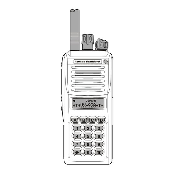
Vertex Standard VX-920 Series Service Manual
Vhf band
Hide thumbs
Also See for VX-920 Series:
- Service manual (68 pages) ,
- Operating manual (40 pages) ,
- Specifications (2 pages)
Table of Contents
Advertisement
Quick Links
Download this manual
See also:
Operating Manual
VX-920 Series
VHF Band
Service Manual
©2005 VERTEX STANDARD CO., LTD.
Specifications ...................................................................................................................................................... 2
Exploded View & Miscellaneous Parts .......................................................................................................... 3
Block Diagram .................................................................................................................................................... 5
Circuit Description ............................................................................................................................................. 7
Alignment .......................................................................................................................................................... 11
Board Units (Schematics, Layouts & Parts)
Main Unit .................................................................................................................................................... 15
Display Unit ................................................................................................................................................ 37
Cable Unit.................................................................................................................................................... 43
EC033N90A
Introduction
This manual provides the technical information necessary for servicing the
VX-920 Series Transceiver.
Servicing this equipment requires expertise in handing surface-mount chip
components. Attempts by non-qualified persons to service this equipment
may result in permanent damage not covered by the warranty, and may be
illegal in some countries.
Two PCB layout diagrams are provided for each double-sided board in this
transceiver. Each side of the board is referred to by the type of the majority of
components installed on that side ("Side A" or "Side B"). In most cases one
side has only chip components (surface-mount devices), and the other has
either a mixture of both chip and leaded components (trimmers, coils, elec-
trolytic capacitors, ICs, etc.), or leaded components only.
As described in the pages to follow, the advanced microprocessor design of
the VX-920 Series Transceiver allows a complete alignment of this transceiver
to be performed without opening the case of the radio; all adjustments can
be performed from the front panel, using the "Alignment Mode" menu.
While we believe the information in this manual to be correct, VERTEX STAN-
DARD assumes no liability for damage that may occur as a result of typo-
graphical or other errors that may be present. Your cooperation in pointing
out any inconsistencies in the technical information would be appreciated.
VERTEX STANDARD CO., LTD.
4-8-8 Nakameguro, Meguro-Ku, Tokyo 153-8644, Japan
VERTEX STANDARD
US Headquarters
10900 Walker Street, Cypress, CA 90630, U.S.A.
YAESU EUROPE B.V.
P.O. Box 75525, 1118 ZN Schiphol, The Netherlands
YAESU UK LTD.
Unit 12, Sun Valley Business Park, Winnall Close
Winchester, Hampshire, SO23 0LB, U.K.
VERTEX STANDARD HK LTD.
Unit 5, 20/F., Seaview Centre, 139-141 Hoi Bun Road,
Kwun Tong, Kowloon, Hong Kong
1
Advertisement
Table of Contents

Related Manuals for Vertex Standard VX-920 Series


Summary of Contents for Vertex Standard VX-920 Series
- Page 1 ICs, etc.), or leaded components only. As described in the pages to follow, the advanced microprocessor design of the VX-920 Series Transceiver allows a complete alignment of this transceiver to be performed without opening the case of the radio; all adjustments can be performed from the front panel, using the “Alignment Mode”...
-
Page 2: Specifications
Specifications General Frequency range: 134-174 MHz Channel / Group: 48 CH / 3 Groups (w/o LCD version) 512 CH / 32 Groups (w/ LCD version) Channel Spacing: 12.5/15/20/25/30 kHz PLL Stepping: 1.25/2.5/5/6.25/7.5 kHz Power Supply Voltage: 7.4 V Current Consumption: 30 mA (Standby w/saver) (Approx. -
Page 3: Exploded View & Miscellaneous Parts
Exploded View & Miscellaneous Parts RA0601800 SIDE COVER CP8249003 Œ PANEL ASSY (16 KEY) Œ RA0745400 (x2 pcs) RA0611500 COIL SPRING ROTARY KNOB (CH) Ž RA0601700 ROTARY KNOB (VOL) RA0688700 LATCH NAIL RA060400B LATCH PLATE “ RA0662800 “ RUBBER KNOB (16KEY) RA0727300 RA068970A FRAME... - Page 4 Exploded View & Miscellaneous Parts Note...
- Page 5 Block Diagram Main Unit...
- Page 6 Block Diagram Display Unit...
-
Page 7: Receiver System
Circuit Description 1. Circuit Configuration by Frequency filter CF1001 (wide channels), CF1002 (narrow chan- The receiver is a double-conversion superhetero- nels) to strip away all but the desired signal, and is dyne type, with a first Intermediate Frequency (IF) applied to the limiter amplifier in Q1067 of 50.85 MHz and a second IF of 450 kHz. - Page 8 Circuit Description fier Q1071 (2SC4617), and noise detector D1047/ nal passes through the limiter and splatter filter of D1048 (both DA221). When a carrier is not being Q1032 (AK2345), and is adjusted for proper devia- received, the noise components passed from de- tion at Q1020 (M62364FP).
- Page 9 Circuit Description tector Q1072 (NJM12902V) is compared with the ref- control voltage from PLL IC Q1070 (SA7025DK). The erence voltage and amplified by the power control negative voltage is fed to the varactor diode after amplifier Q1072 (NJM12902V). The output from c o n ve r s i o n t o a n e g a t i ve va l u e a t Q 1 0 3 1 Q1072 (NJM12902V) controls the gate bias of the fi- (NJM2130F), using the output voltage of the D/A...
- Page 10 Circuit Description Note...
-
Page 11: Required Test Equipment
Alignment Introduction The following test equipment (and thorough famil- The VX-920 series is carefully aligned at the factory iarity with its correct use) is necessary for complete for the specified performance across the frequency realignment. Correction of problems caused by mis- range specified for each version. -
Page 12: Alignment Preparation & Precautions
Alignment Alignment Preparation & Precautions Setup the test equipment as shown for transceiver A 50-Ohm RF Dummy Load and in-line wattmeter alignment, apply 7.5 V DC power to the transceiver. must be connected to the main antenna jack in all Refer to the drawings above for Alignment Points. -
Page 13: Basic Alignment Mode
Install the CE59 (version 2.06 or later) to your PC. entire radio. The value of each parameter can be The re-alignment for VX-920 series uses the changed to the desired position by use of the “ ” / “Alignment“ menu of CE59. - Page 14 Alignment CH (C ) Fine Alignment Mode HANNEL HANNEL The CH Fine Alignment Mode allows you to align the radio separately for every operating channel. The value of each parameter can be changed to the de- sired position using the “ ” / “ ” and up/down arrow keys, direct number input, and by dragging the PC mouse.
-
Page 15: Main Unit
Main Unit Circuit Diagram RX MAIN: 0 V RX SUB: 2.7 V TX: –0.5 V 0.3 dBµV emf –9.0 dBµV emf @154.1 MHz RX: 2.6 V @154.1 MHz RX: 2.0 V RX: 4.8 V RX: 4.9 V TX: 0 V TX: 0 V TX: 0 V TX: 0 V... - Page 16 Main Unit Note...
- Page 17 Main Unit Parts Layout (Side A) M62364FP LA8630M BD6111FV 2SA1774 (FR) RTM002P02 (BA) DTC114TE (04) NJM2130F (BA) TC7S08FU (E2) UNR911FJ0L (6O) (Q1020) (Q1023) (Q1028) (Q1012, 1036) (Q1088) (Q1009, 1013, 1039, (Q1031) (Q1085) (Q1026) 1046, 1050, 1053, BR93L66RFVM 1054, 1057, 1059, (Q1065) 1064) LM2904PWR...
- Page 18 Main Unit Parts Layout (Side B) AK2345 CD4066BPWR SA7025DK 2SK508 (K52) 2SK3478 2SC3356 (R24) DTC114TE (04) UNR911FJ0L (6O) DA221 (K) (Q1032) (Q1078) (Q1070) (Q1047) (Q1021) (Q1027) (Q1040, 1048) (Q1045) (D 1023, 1039, 1047, 1048) LM2902PWR 2SK880GR (XG) 2SC4227 (R32) (Q1073, 1074) (Q1068) (Q1052) NJU4066BV...
-
Page 19: Parts List
Main Unit Parts List REF. DESCRIPTION VALUE TOL. MFR’S DESIG VXSTD P/N VERS. LOT. SIDE LAY ADR PCB with Components CB2254001 Printed Circuit Board AC033N000 FR0122600 C 1001 CHIP CAP. 150pF GRM1552C1H151JA01D K22178240 C 1003 CHIP CAP. 0.001uF GRM155B11H102KA01D K22178809 C 1004 CHIP CAP. - Page 20 Main Unit Parts List REF. DESCRIPTION VALUE TOL. MFR’S DESIG VXSTD P/N VERS. LOT. SIDE LAY ADR C 1068 CHIP TA.CAP. 10uF 6.3V TEMSVA0J106M-8R K78080027 C 1069 CHIP CAP. 15pF GRM1552C1H150JZ01D K22178216 C 1070 CHIP CAP. 10pF GRM1552C1H100JZ01D K22178212 C 1073 CHIP CAP. 0.01uF GRM36B103K16PT K22128804...
- Page 21 Main Unit Parts List REF. DESCRIPTION VALUE TOL. MFR’S DESIG VXSTD P/N VERS. LOT. SIDE LAY ADR C 1141 CHIP CAP. 0.01uF GRM36B103K16PT K22128804 C 1142 CHIP CAP. 0.01uF GRM36B103K16PT K22128804 C 1143 CHIP CAP. 12pF GRM1552C1H120JZ01D K22178214 C 1144 CHIP TA.CAP. 4.7uF 6.3V TESVSP0J475M-8R...
- Page 22 Main Unit Parts List REF. DESCRIPTION VALUE TOL. MFR’S DESIG VXSTD P/N VERS. LOT. SIDE LAY ADR C 1215 CHIP CAP. 150pF GRM1552C1H151JA01D K22178240 C 1216 CHIP CAP. 0.01uF GRM36B103K16PT K22128804 C 1217 CHIP CAP. 0.001uF GRM155B11H102KA01D K22178809 C 1218 CHIP TA.CAP. TMCSA1C105MTR K78120023 C 1219 CHIP CAP.
- Page 23 Main Unit Parts List REF. DESCRIPTION VALUE TOL. MFR’S DESIG VXSTD P/N VERS. LOT. SIDE LAY ADR C 1288 CHIP CAP. 0.1uF GRM36B104K10PT K22108802 C 1289 CHIP CAP. 0.001uF GRM155B11H102KA01D K22178809 C 1290 CHIP CAP. 0.001uF GRM155B11H102KA01D K22178809 C 1291 CHIP CAP. 0.01uF GRM36B103K16PT K22128804...
- Page 24 Main Unit Parts List REF. DESCRIPTION VALUE TOL. MFR’S DESIG VXSTD P/N VERS. LOT. SIDE LAY ADR C 1354 CHIP CAP. 0.001uF GRM155B11H102KA01D K22178809 C 1355 CHIP CAP. 0.001uF GRM155B11H102KA01D K22178809 C 1356 CHIP CAP. 0.047uF GRM36B473K10PT K22108801 C 1357 CHIP CAP. 22pF GRM1552C1H220JZ01D K22178220...
- Page 25 Main Unit Parts List REF. DESCRIPTION VALUE TOL. MFR’S DESIG VXSTD P/N VERS. LOT. SIDE LAY ADR C 1428 CHIP CAP. 0.1uF GRM36B104K10PT K22108802 C 1429 CHIP CAP. 0.001uF GRM155B11H102KA01D K22178809 C 1430 CHIP CAP. 0.1uF GRM36B104K10PT K22108802 C 1432 CHIP CAP. 0.001uF GRM155B11H102KA01D K22178809...
- Page 26 Main Unit Parts List REF. DESCRIPTION VALUE TOL. MFR’S DESIG VXSTD P/N VERS. LOT. SIDE LAY ADR D 1051 DIODE 1SV323(TPH3) G2071006 D 1052 DIODE 1SV323(TPH3) G2071006 F 1001 CHIP FUSE 0434 003. 3.0A Q0000107 FB1001 FERRITE BEADS SMB304729 L9190094 FB1002 FERRITE BEADS BLM21A121SPT L9190108...
- Page 27 Main Unit Parts List REF. DESCRIPTION VALUE TOL. MFR’S DESIG VXSTD P/N VERS. LOT. SIDE LAY ADR L 1056 M.RFC 33uH FLC32T-330J L1690221 L 1057 M.RFC 0.15uH HK1608 R15J-T L1690938 Q 1001 IC CD4053BPWR G1093864 Q 1001 IC NJU4053BV-TE1 G1092927 Q 1002 TRANSISTOR XP1501-(TX) G3070143...
- Page 28 R 1025 CHIP RES. 1/16W 5% RMC1/16S 102JTH J24189025 R 1026 CHIP RES. 1/16W 5% RMC1/16S 102JTH J24189025 R 1027 CHIP RES. 220k 1/16W 5% RMC1/16S 224JTH J24189053 R 1028 CHIP RES. 1/16W 5% RMC1/16S 102JTH J24189025 : Please contact VERTEX STANDARD...
- Page 29 Main Unit Parts List REF. DESCRIPTION VALUE TOL. MFR’S DESIG VXSTD P/N VERS. LOT. SIDE LAY ADR R 1029 CHIP RES. 2.2k 1/16W 5% RMC1/16S 222JTH J24189029 R 1030 CHIP RES. 1/16W 5% RMC1/16S JPTH J24189070 R 1031 CHIP RES. 0.33 1/8W RMC1/8 R33KTP...
- Page 30 Main Unit Parts List REF. DESCRIPTION VALUE TOL. MFR’S DESIG VXSTD P/N VERS. LOT. SIDE LAY ADR R 1095 CHIP RES. 220k 1/16W 5% RMC1/16S 224JTH J24189053 R 1097 CHIP RES. 1/16W 5% RMC1/16S 223JTH J24189041 R 1098 CHIP RES. 1/16W 5% RMC1/16S 563JTH J24189046...
- Page 31 Main Unit Parts List REF. DESCRIPTION VALUE TOL. MFR’S DESIG VXSTD P/N VERS. LOT. SIDE LAY ADR R 1160 CHIP RES. 1/16W 5% RMC1/16S 561JTH J24189022 R 1163 CHIP RES. 680k 1/16W 5% RMC1/16S 684JTH J24189059 R 1164 CHIP RES. 1/16W 5% RMC1/16S 103JTH J24189037...
- Page 32 Main Unit Parts List REF. DESCRIPTION VALUE TOL. MFR’S DESIG VXSTD P/N VERS. LOT. SIDE LAY ADR R 1230 CHIP RES. 1/16W 5% RMC1/16S 473JTH J24189045 R 1231 CHIP RES. 1/16W 5% RMC1/16S JPTH J24189070 R 1232 CHIP RES. 680k 1/16W 5% RMC1/16S 684JTH J24189059...
- Page 33 Main Unit Parts List REF. DESCRIPTION VALUE TOL. MFR’S DESIG VXSTD P/N VERS. LOT. SIDE LAY ADR R 1301 CHIP RES. 220k 1/16W 5% RMC1/16S 224JTH J24189053 R 1302 CHIP RES. 3.3k 1/16W 5% RMC1/16S 332JTH J24189031 R 1303 CHIP RES. 470k 1/16W 5% RMC1/16S 474JTH...
- Page 34 Main Unit Parts List REF. DESCRIPTION VALUE TOL. MFR’S DESIG VXSTD P/N VERS. LOT. SIDE LAY ADR R 1364 CHIP RES. 1/16W 5% RMC1/16S 102JTH J24189025 R 1365 CHIP RES. 1/16W 5% RMC1/16S 102JTH J24189025 R 1366 CHIP RES. 1/16W 5% RMC1/16S 102JTH J24189025 R 1367 CHIP RES.
- Page 35 Main Unit Parts List REF. DESCRIPTION VALUE TOL. MFR’S DESIG VXSTD P/N VERS. LOT. SIDE LAY ADR R 1426 CHIP RES. 100k 1/16W 5% RMC1/16S 104JTH J24189049 R 1427 CHIP RES. 1/16W 5% RMC1/16S 473JTH J24189045 R 1428 CHIP RES. 1/16W 5% RMC1/16S 123JTH J24189038...
- Page 36 Main Unit Parts List REF. DESCRIPTION VALUE TOL. MFR’S DESIG VXSTD P/N VERS. LOT. SIDE LAY ADR S 1001 TACT SWITCH SKRTLAE010 N5090130 S 1002 TACT SWITCH SKRTLAE010 N5090130 S 1003 TACT SWITCH SKRTLAE010 N5090130 S 1004 TACT SWITCH SKRTLAE010 N5090130 S 1005 TACT SWITCH SKRTLAE010...
-
Page 37: Display Unit
Display Unit Circuit Diagram PWR ON: 5.0 V PWR OFF: 0 V 7.4 V 3.8 V @25 °C 6.3 V LAMP ON: 3.1 V LAMP OFF: 3.7 V PWR ON: 3.2 V PWR OFF: 0 V 2.9 V @25 °C LAMP ON: 3.1 V LAMP ON: 1.3 V LAMP OFF: 3.9 V... - Page 38 Display Unit Note...
- Page 39 Display Unit Parts Layout (Side A)
- Page 40 Display Unit Parts Layout (Side B) NJU6624AFG1 2SA1602 (MF) DTC114TE (04) XP1501 (5R) TAR5S50U (Q2006) (Q2005) (Q2001, 2002) (Q2004) (Q2003)
- Page 41 Display Unit Parts List REF. DESCRIPTION VALUE TOL. MFR’S DESIG VXSTD P/N VERS. LOT. SIDE LAY ADR PCB with Components CB2255001 LCD: ON Printed Circuit Board AC033N000 FR0123200 C 2001 CHIP CAP. 0.1uF GRM36B104K10PT K22108802 C 2002 CHIP CAP. 0.01uF GRM36B103K16PT K22128804 C 2003 CHIP CAP.
- Page 42 Display Unit Parts List REF. DESCRIPTION VALUE TOL. MFR’S DESIG VXSTD P/N VERS. LOT. SIDE LAY ADR R 2018 CHIP RES. 1/16W 5% RMC1/16S 102JTH J24189025 R 2019 CHIP RES. 1/16W 5% RMC1/16S 102JTH J24189025 R 2020 CHIP RES. 1/16W 5% RMC1/16S 102JTH J24189025 R 2021 CHIP RES.
-
Page 43: Cable Unit
Cable Unit Circuit Diagram Parts Layout Parts List REF. DESCRIPTION VALUE TOL. MFR’S DESIG VXSTD P/N VERS. LOT. SIDE LAY ADR Printed Circuit Board AC033N000 FR013220C C 5001 CHIP CAP. 0.001uF GRM188B11H102KA01D K22174821 C 5002 CHIP CAP. 0.001uF GRM188B11H102KA01D K22174821 MC5001 MIC. - Page 44 Copyright 2004 VERTEX STANDARD CO., LTD. All rights reserved No portion of this manual may be reproduced without the permission of VERTEX STANDARD CO., LTD.
Need help?
Do you have a question about the VX-920 Series and is the answer not in the manual?
Questions and answers