
Related Manuals for Sony FD Triniton KD-28DX40U


Summary of Contents for Sony FD Triniton KD-28DX40U
-
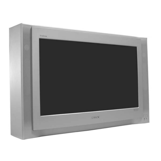
Page 1: Service Manual
SERVICE MANUAL FE-2 CHASSIS MODEL MODEL COMMANDER DEST CHASSIS NO. COMMANDER DEST CHASSIS NO. KD-28DX40U KD-32DX40U RM-933 SCC-Q52K-A RM-933 SCC-Q52L-A KD-28/32DX40 RM-933 - 1 -... -
Page 2: Table Of Contents
TANCE CRITIQUE POUR LA SÈCURITÈ DU FONCTIONNEMENT, THESE COMPONENTS WITH SONY PARTS WHOSE PART NE LES REMPLACER QUE PAR DES COMPSANTS SONY DONT NUMBERS APPEAR AS SHOWN IN THIS MANUAL OR IN LE NUMÈRO DE PIÈCE EST INDIQUÈ DANS LE PRÈSENT SUPPLEMENTS PUBLISHED BY SONY. - Page 3 l l a l l a . s l . s l . s l . s l e i l i n i WARNING (UK Models only) The flexible mains lead is supplied connected to a B.S. 1363 fused plug having a fuse of 5 AMP rating.
-
Page 4: Connectors
21 pin connector Pin No Signal Signal level Audio output B Standard level : 0.5V rms (right) Output impedence : Less than 1kohm* Audio output B Standard level : 0.5V rms (right) Output impedence : More than 10kohm* Audio output A Standard level : 0.5V rms (left) Output impedence : Less than 1kohm*... -
Page 5: Self Diagnostic Software
FE-2 SELF DIAGNOSTIC SOFTWARE The identification of errors within the FE-2 chassis is triggered in one of two ways :- 1: Busy or 2: Device failure to respond to IIC. In the event of one of these situations arising the software will first try to release the bus if busy (Failure to do so will report with a continuous flashing LED) and then communicate with each device in turn to establish if a device is faulty. -
Page 6: Automatically Tuning The Tv
Getting Started Basic Operation 5. Automatically tuning the TV Selecting Digital or analogue mode Press the DIGITAL/ button on the remote control to switch between Digital and analogue mode. To 1. When you switch on the TV for the first time a menu appears on the check if you are watching a Digital or analogue mode press the PROG +/- button. -
Page 7: Viewing Digital Teletext
Basic Operation Basic Operation The Category pop-up list Viewing Digital Teletext The ‘Category’ pop-up list allows you to quickly search for a programme by choosing from different Many broadcasters now provide a Digital Teletext service in the form of a dedicated Teletext channel. VIDEO categories of programmes. -
Page 8: Teletext(Analogue)
Basic Operation Basic Operation Teletext (Analogue) The Digital EPG menu Most analogue TV channels broadcast a Teletext service. The index page (usually page 100) provides The EPG menu (Electronic Programme Guide) provides you with a quick and easy way to:- information on how to use the service. -
Page 9: The Digital Info Display
Basic Operation Advanced Operation Detail Set-up The Digital INFO display VIDEO This menu gives you information on the programmes currently being shown aswell as the those The ‘Detail Set-up’ menu allows you to further customise your TV with the following features: DIGITAL programmes which are on next. -
Page 10: The Tv Menu System
This TV contains a menu system which is based on a series of user friendly on-screen displays. These Periodically Sony issues updates for the software that controls your TV. This feature allows you to displays will help you to get the most from your TV, helping you to change the picture settings, sound automatically receive updates free through your existing aerial. -
Page 11: The Set Up Menu
Advanced Operation Advanced Operation 5. Highlight and activate one of the options using the v and b buttons, then press the v or V buttons to The Set Up menu set the option to On or Off. See the table below for an explanation of each option and their effects. The ‘Set Up’... -
Page 12: Remote Control Of Equipment
Remote control of connected equipment Troubleshooting This remote control can operate not only Sony DVDs and VCRs, but also those made by other Here are some simple soloutions to problems which may affect the picture and sound. manufacturers. The following instructions will guide you through the set up procedure. -
Page 13: Disassembly
SECTION 2 DISASSEMBLY 2-1. Rear Cover Removal 2-2. Side Control Module Removal <= => Screws => <= => <= <= Remove the rear cover fixing screws indicated and withdraw Remove the two screws fixing the user control module to the the rear cover from the beznet. -
Page 14: Service Position
2-4. Service Position 2-5. F6 and H8 Board Removal Clip Clips Position the chassis as indicated to access the solder side Release the clip circled and pull the F6 bracket towards the of the PWB’s. To gain access to the A Board follow the rear of the set. -
Page 15: Picture Tube Removal
2-7. Picture Tube Removal WARNING: BEFORE REMOVING THE ANODE CAP High voltage remains in the CRT even after the power is disconnected. To avoid electric shock, discharge CRT before attempting to remove the anode cap. Short between anode and CRT coated earth ground strap. -
Page 16: Bottom Plates
REMOVAL AND REPLACEMENT OF THE MAIN BRACKET For safety reasons, on no account should the plates be re- moved and not refitted after servicing. BOTTOM PLATES. (1) REMOVING THE PLATES (2) REFITTING THE PLATES In the event of servicing being required to the solder side of the D Board printed wiring board, the Because the plates differ in size it is important that the correct plates are refitted in their original bottom plates fitted to the main chassis bracket require to be removed. -
Page 17: Set-Up Adjustments
SECTION 3 SET-UP ADJUSTMENTS • Carry out the adjustments in the following order : When complete readjustment is necessary or a new picture 3-1. Beam Landing. tube is installed, carry out the following adjustments. 3-2. Convergence. • Unless there are specific instructions to the contrary, carry 3-3. -
Page 18: Convergence
If the V.STAT magnet is moved in the direction of the (a) 3-2. Convergence and (b) arrows, the Red, Green and Blue points move as indicated below. Preparation: • Before starting this adjustment, adjust the focus, horizontal size and vertical size. •... - Page 19 Geometry Adjustment. YCH Adjustment Preparation: YCH VR Before starting this adjustment, adjust the horizontal and Deflection Yoke vertical static convergence. Remove the deflection yoke spacer. Tilt the deflection yoke as indicated in the figure below and TLV Adjustment optimise the geometry. Tilting the DY Up and Down will balance the upper and lower pin adjustment.
-
Page 20: Focus Adjustment
Layout of each control 3-4. Screen (G2), White Balance [Adjustment in the service mode using the remote commander] G2 adjustment Input a dot signal from the pattern generator. Enter the ‘Service Mode’ by pressing ‘TEST’, ‘TEST’ and ‘38’ (TT-38) on the remote commander, to set up the G2 V.STAT service adjustment mode. -
Page 21: Circuit Adjustments
SECTION 4 CIRCUIT ADJUSTMENTS 4-1. Electrical Adjustments Service adjustments to this model can be performed using the supplied remote Commander RM-932. How to enter into the Service Mode Turn on the main power switch and enter into the stand-by mode. Press the following sequence of buttons on the Remote Commander. - Page 22 Sub Colour Adjustment Deflection System Adjustment Enter into the ‘Geometry’ service menu. Receive a PAL colour bar signal. Select and adjust each item in order to obtain the optimum image. Connect an oscilloscope to Pin 5 of CN003 [A Board]. Enter into the ‘Service’...
-
Page 23: Test Mode
4-2. TEST MODE 1: Test Mode 1 is available by pressing the ‘TEST’ button once, OSD ‘T’ appears. The functions described below are available by selecting the indicated keys. The ‘T’ is released automatically after each < > command is executed. y t i s i l i n i... -
Page 24: Block Diagrams
5-1. BLOCK DIAGRAMS (1) CN1701 V-PULSE QP OUT IC1902 DF/DQP/TIMING Q1841 CN1718 Q.P.- LOW B A BOARD IC1701 CN510 Q.P.+ Q.P. VM AMP VM OUT VM AMP VM OUT BUFFER Q1701 Q1708, 1711 Q1704, 1705 NECK ASSY IC1901 CN1702 COMPARATOR 15V PULSE A BOARD CN503... -
Page 25: Block Diagrams
5-1. BLOCK DIAGRAMS (2) CN510 VOUT VMOUT CN1203 TO B BOARD TO VM BOARD CN8302 CN1701 MUTE IC604 WFR L IN PH601 DUAL DC REGULATOR ISOLATOR WFR R IN CN606 AC IN LOWB CN1202 TO F3 BOARD LINE FILTER MAIN RECT IC001 AC IN T601... -
Page 26: Block Diagrams
5-1. BLOCK DIAGRAMS (3) CN4101 CN707 RIGHT R.G.B. OUT LEFT CN706 FBLK CVBS LED DRIVER TU4101 3.3V IC4101 Q4103 J701 PLL 12C 5W IC701 CONT A O/PA CN703 R.G.B. DRIVE CONT D O/PA G IN Q4101 Q4102 I/PD CONT B B IN SCL (TV) PICTURE TUBE... -
Page 27: Circuit Board Location
5-2. CIRCUIT BOARD LOCATION Reference Information RESISTOR : METAL FILM : SOLID FPRD : NON FLAMMABLE CARBON C Board FUSE : NON FLAMMABLE FUSIBLE : NON FLAMMABLE METAL OXIDE VM Board : NON FLAMMABLE CEMENT B Board : NON FLAMMABLE WIREWOUND CVM Board N Board S1 Board... - Page 28 A Board IC Voltage Table A Board Semiconductor Voltage Table ~ A Board Waveforms ~ 20us/div 20us/div 1.88 Vp-p (H) 1.84 Vp-p (H) 20us/div 20us/div 1.86 Vp-p (H) 6.0 Vp-p (H) 20us/div 20us/div 5.4 Vp-p (H) 16.8 Vp-p (H) A Board Difference Table 20us/div 5ms/div 1.83 Vp-p (V)
- Page 29 KD-28/32DX40U 9-927-411-01 A Schematic [ Power Supply, Deflection, Small Signal, Audio Amp ] page 1/2 ~ - 29 -...
- Page 30 KD-28/32DX40U 9-927-411-01 A Schematic [ Power Supply, Deflection, Small Signal, Audio Amp ] page 2/2 ~ - 30 -...
- Page 31 ~ A Board Semiconductor Location Table ~ NOTE: Portions of the circuit marked as shown are high voltage areas. Use care to prevent electric shock during inspection or repair. ~ A Printed Wiring Board Conductor side ~ - 31 -...
- Page 32 ~ C Board Schematic [ R-G-B Out ] ~ ~ VM Printed Wiring Board ~ ~ C Printed Wiring Board ~ ~ C Board Waveforms ~ 10us/div 10us/div 2.16 Vp-p (H) 2.0 Vp-p (H) 10us/div 10us/div 1.9 Vp-p (H) 6.8 Vp-p (H) 10us/div 10us/div ~ C Board Semiconductor Voltages ~...
- Page 33 VM Board Waveforms ~ 5ms/div 5ms/div 5ms/div 1.54 Vp-p (V) 1.4 Vp-p (V) 20 Vp-p (H) VM Board Semiconductor Voltages ~ VM Schematic [ Velocity Modulation ] ~ [Dynamic Focus and DQP ] - 33 -...
- Page 34 A1 Schematic [ Digital Front End Processing ] ~ - 34 -...
- Page 35 ~ A1 Printed Wiring Board Conductor side A ~ ~ A1 Board Semiconductor Location Table (side A) ~ ~ A1 Printed Wiring Board Conductor side B ~ ~ A1 Board Semiconductor Location Table (side B) ~ - 35 -...
- Page 36 B Schematic [ Y.U.V. Switching ] ~ B Printed Wiring Board ~ H2 Schematic [ Y/C In, Audio In, Headphone In ] ~ H2 Printed Wiring Board ~ - 36 -...
- Page 37 D3 Schematic [ 4:3 Switching ] ~ H8 Schematic [ LED and SIRCS Response ] ~ F3 Schematic [ AC Input, Fuse ] ~ F3 Printed Wiring Board ~ H8 Printed Wiring Board ~ D3 Printed Wiring Board ~ F6 Schematic [ Power Switch ] ~ D2 Schematic [ Smart Mode Deflection ] ~ D2 Printed Wiring Board ~ F6 Printed Wiring Board ~...
-
Page 38: Semiconductors
5-4. SEMICONDUCTORS TCET1103G BC327-25 BAS316-115 UDZSTE-175.6B BA09T L78L33ABZ-AP PQ3RF33 LM2940T-9.0 PQ05RF11 SARS01V0 UDZSTE-176.8B SE-012N-LF4 DTZ-TT11-6.8B UDZSTE-179.1B UPC2405AHF UDZS-TE17-33B 1SS355TE-17 ANODE CATHODE TDA6108JF/N1B 1 : V IN 2 : V OUT 3 : GND 4 : ON/OFF CONTROL DAN202K BU2515DX-127 MCZ3001D PST573IMT-T1 TC74HC4066AF CXA1875AM-T4... - Page 39 D2SB60A-F04 L59SRSGC-CC TLG124A UGB8BT MA3047M-TX D4SBL20UF1 D4SB60LF GBU4JL-6088 2SA2005 MM3Z12VT1 MM3Z4V7T1 MM3Z6V8T1 ERA38-06 RD15ES-B2 HZS9-1NB2 RD3.6ES-B2 MTZJ-4.7C RD5.1ESB2 MTZJ-7.5B RD5.6ESB2 MTZ-33A RD6.8ES-B2 MTZJ-T-77-9.1A UZ4.7BSC RD10ESB2 1SS119-25 2SB734-34 CATHODE RK14V1 ANODE ERC06-15S RK46LF-T2 RU4AM-T3 2SK2036(TE85L) CATHODE ANODE - 39 -...
-
Page 40: Ic Block Diagrams
5-5 IC BLOCK DIAGRAMS A BOARD IC604 BA41W12ST-V5 A BOARD IC401/IC531 LM393DT Vref A BOARD IC601 MCZ3001D Remote DVLD Internal Driver Sel=34v ref 5v Reg. 10v 15v/8v Level Shift Vsense Control Logic Latch Centre Timer A BOARD IC1201 TDA7495S VOLUME OP AMP MUTE/STBY PROTECTIONS... -
Page 41: Exploded Views
SECTION 6 EXPLODED VIEWS NOTE : Items marked “*” are not stocked Items with no part number and no description are not since they are seldom required for stocked because they are seldom required for routine routine service. Some delay should service. -
Page 42: Picture Tube
6-2. Picture Tube REF.NO. PART.NO DESCRIPTION REMARK REF.NO. PART.NO DESCRIPTION REMARK - 42 -... -
Page 43: Electrical Parts List
SECTION 7 ELECTRICAL PARTS LIST PARTS LISTING TABLE OF CONTENTS Page A1 BOARD COMPLETE Parts List : ..................... 47 A BOARD COMMON Parts List : Parts common to all models listed in this manual ..... 50 A BOARD VARIANT Parts List : Parts that belong only to the model specified Model KD-28DX40... - Page 44 H7 A1 REF.NO. PART.NO DESCRIPTION REMARK REF.NO. PART.NO DESCRIPTION REMARK C4158 1-162-974-11 CERAMIC CHIP 0.01UF *A-1631-157-A A1 Board, Complete C4159 1-162-974-11 CERAMIC CHIP 0.01UF C4160 1-162-974-11 CERAMIC CHIP 0.01UF 1-682-341-11 PWB, A1 C4161 1-162-974-11 CERAMIC CHIP 0.01UF 1-720-213-11 PWB, A1 COMBI C4162 1-162-974-11 CERAMIC CHIP 0.01UF 4-202-373-01 SPRING, IC...
- Page 45 REF.NO. PART.NO DESCRIPTION REMARK REF.NO. PART.NO DESCRIPTION REMARK < DIODE > IC4602 £ 8-749-013-21 IC TLP721(D4-G) IC4603 6-700-293-01 IC SE-012N-LF4 D4101 8-719-982-24 DIODE MTZJ-33A IC4604 8-759-390-57 IC UPC2405AHF D4102 8-719-812-43 DIODE TLG124A IC4605 8-759-069-28 IC PQ05RF11 D4103 8-719-914-43 DIODE DAN202K IC4606 8-759-267-25 IC LM2940T-9.0 D4601...
- Page 46 B1 A1 REF.NO. PART.NO DESCRIPTION REMARK REF.NO. PART.NO DESCRIPTION REMARK R4104 1-216-864-11 SHORT R4167 1-216-833-11 RES-CHIP 1/16W R4105 1-216-864-11 SHORT R4168 1-216-829-11 RES-CHIP 4.7K 5% 1/16W R4106 1-216-864-11 SHORT R4169 1-216-821-11 RES-CHIP 1/16W R4107 1-216-864-11 SHORT R4170 1-216-833-11 RES-CHIP 1/16W R4108 1-216-864-11 SHORT R4171...
- Page 47 A A1 A REF.NO. PART.NO DESCRIPTION REMARK REF.NO. PART.NO DESCRIPTION REMARK < RELAY > C038 1-163-038-91 CERAMIC CHIP 0.1UF C039 1-164-505-11 CERAMIC CHIP 2.2UF RY4601 £ 1-755-388-11 RELAY (AC POWER) C040 1-163-017-00 CERAMIC CHIP 0.0047UF 10.00% 50V C042 1-162-625-11 CERAMIC CHIP 0.0047UF 5.00% 50V <...
- Page 48 REF.NO. PART.NO DESCRIPTION REMARK REF.NO. PART.NO DESCRIPTION REMARK C410 1-162-970-91 CERAMIC CHIP 0.01UF 10.00% 25V C550 1-107-638-11 ELECT 33UF 20.00% 160V C411 1-163-009-91 CERAMIC CHIP 0.001UF 10.00% 50V C552 1-102-212-00 CERAMIC 820PF 10.00% 500V C412 1-164-346-11 CERAMIC CHIP 1UF C553 1-137-417-11 MYLAR 0.0047UF 10.00% 200V...
- Page 49 REF.NO. PART.NO DESCRIPTION REMARK REF.NO. PART.NO DESCRIPTION REMARK C649 1-163-038-91 CERAMIC CHIP 0.1UF D003 8-719-109-69 DIODE RD3.6ES-B2 C657 1-126-952-11 ELECT 1000UF 20.00% 35V D005 8-719-929-15 DIODE HZS9.1NB2 C1201 1-216-952-91 ELECT 1000UF 20.00% 35V D006 8-719-109-89 DIODE RD5.6ESB2 C1202 1-126-959-11 ELECT 0.47UF 20.00% 50V D007...
- Page 50 REF.NO. PART.NO DESCRIPTION REMARK REF.NO. PART.NO DESCRIPTION REMARK D423 8-719-081-98 DIODE MM3Z6V8T1 < FERRITE BEAD > D424 8-719-069-60 DIODE UDZSTE-179.1B D427 8-719-082-01 DIODE MM3Z12VT1 FB601 1-410-397-21 FERRITE 1.1UH D428 8-719-978-33 DIODE DTZ-TT11-6.8B FB602 1-410-397-21 FERRITE 1.1UH D429 8-719-978-33 DIODE DTZ-TT11-6.8B FB603 1-412-911-11 FERRITE FB604...
- Page 51 REF.NO. PART.NO DESCRIPTION REMARK REF.NO. PART.NO DESCRIPTION REMARK L404 1-410-993-42 INDUCTOR Q607 8-729-053-36 TRANSISTOR 2SK2640-01MR L405 1-535-143-61 LEAD, JUMPER (5.0MM) Q608 8-729-120-28 TRANSISTOR 2SC1623-L5L6 L406 1-414-177-11 INDUCTOR Q609 8-729-026-49 TRANSISTOR 2SA1037AK-T146 L410 1-216-025-11 RES-CHIP 1/10W Q1230 8-729-027-56 TRANSISTOR DTC143TKA-T146 L430 1-412-002-31 INDUCTOR 4.7UH Q1231...
- Page 52 REF.NO. PART.NO DESCRIPTION REMARK REF.NO. PART.NO DESCRIPTION REMARK R012 1-216-121-91 RES-CHIP 1/10W R103 1-216-061-91 RES-CHIP 3.3K 5% 1/10W R014 1-216-069-00 RES-CHIP 6.8K 5% 1/10W R104 1-216-295-91 SHORT R015 1-216-198-91 RES-CHIP 1/8W R105 1-414-813-11 FERRITE R017 1-216-025-11 RES-CHIP 1/10W R106 1-215-900-11 METAL OXIDE R018 1-208-820-11 METAL CHIP 0.5% 1/10W...
- Page 53 REF.NO. PART.NO DESCRIPTION REMARK REF.NO. PART.NO DESCRIPTION REMARK R419 1-216-022-00 RES-CHIP 1/10W R523 1-216-121-11 RES-CHIP 1/10W R420 1-216-073-91 RES-CHIP 1/10W R524 1-216-075-00 RES-CHIP 1/10W R421 1-216-049-11 RES-CHIP 1/10W R525 1-216-057-00 RES-CHIP 2.2K 5% 1/10W R422 1-216-829-11 RES-CHIP 4.7K 5% 1/16W R526 1-216-089-91 RES-CHIP 1/10W...
- Page 54 H5 D2 REF.NO. PART.NO DESCRIPTION REMARK REF.NO. PART.NO DESCRIPTION REMARK R632 1-249-417-11 CARBON 1/4W T602 £ 1-431-732-31 TRANSFORMER, CONVERTER (SRT) R633 1-215-481-00 METAL 330K 1% 1/4W T603 £ 1-435-976-11 TRANSFORMER, CONVERTER (PIT) R634 1-217-625-00 METAL 0.05 10% R635 1-260-300-11 CARBON 1/2W <...
- Page 55 REF.NO. PART.NO DESCRIPTION REMARK REF.NO. PART.NO DESCRIPTION REMARK C555 1-127-717-11 FILM 19000PF 3.00% 1.2KV Q8307 8-729-120-28 TRANSISTOR 2SC1623-L5L6 < RESISTOR > < RESISTOR > JR101 1-216-295-91 SHORT R8301 1-216-809-11 RES-CHIP 1/16W R8302 1-216-809-11 RES-CHIP 1/16W R022 1-216-689-11 RES-CHIP 1/10W R8303 1-216-809-11 RES-CHIP 1/16W R053...
- Page 56 REF.NO. PART.NO DESCRIPTION REMARK REF.NO. PART.NO DESCRIPTION REMARK < VARISTOR > D1802 8-719-110-17 DIODE RD10ESB2 D1803 8-719-110-17 DIODE RD10ESB2 VD3601 1-803-830-11 VARISTOR (ERZ14D621) < IC > *A-1624-106-A F6 Board, Complete IC701 8-759-562-43 IC TDA6108JF/N1B 1-682-339-15 PWB, F6 IC1801 8-759-603-37 IC M5216P <...
- Page 57 REF.NO. PART.NO DESCRIPTION REMARK REF.NO. PART.NO DESCRIPTION REMARK < DIODE > < RESISTOR > D2801 8-719-991-33 DIODE 1SS133T-77 JR8801 1-216-864-11 SHORT < TRANSISTOR > R8803 1-249-441-11 CARBON 100K 5% 1/4W R8804 1-216-825-11 RES-CHIP 2.2K 5% 1/16W Q2801 8-729-119-78 TRANSISTOR 2SC2785-HFE R8805 1-216-833-11 RES-CHIP 1/16W...
- Page 58 REF.NO. PART.NO DESCRIPTION REMARK REF.NO. PART.NO DESCRIPTION REMARK C1959 1-136-169-00 FILM 0.22UF 5.00% 50V Q1707 8-729-049-09 TRANSISTOR BC327-25 Q1708 8-729-045-05 TRANSISTOR 2SA2005 < CONNECTOR > Q1709 8-729-119-78 TRANSISTOR 2SC2785-HFE Q1710 8-729-049-10 TRANSISTOR BC337-25 CN1701 1-691-771-11 PLUG (MICRO CONNECTOR) 9P Q1711 8-729-045-04 TRANSISTOR 2SC5511 CN1702 *1-564-506-11 PLUG, CONNECTOR 3P...
- Page 59 REF.NO. PART.NO DESCRIPTION REMARK REF.NO. PART.NO DESCRIPTION REMARK R1960 1-216-833-11 RES-CHIP 1/16W R1908 1-216-813-11 RES-CHIP 1/16W R1961 1-216-839-11 RES-CHIP 1/16W R1909 1-215-489-00 METAL 680K 1% 1/4W R1910 1-216-864-11 SHORT VM Board Variant Parts KD-32DX40 R1911 1-216-833-11 RES-CHIP 1/16W R1912 1-216-857-11 RES-CHIP 1/16W <...
- Page 60 H2 H8 REF.NO. PART.NO DESCRIPTION REMARK REF.NO. PART.NO DESCRIPTION REMARK L903 1-408-603-31 INDUCTOR 10UH R7152 1-216-829-11 RES-CHIP 4.7K 5% 1/16W L904 1-410-119-11 INDUCTOR R7153 1-216-829-11 RES-CHIP 4.7K 5% 1/16W R7154 1-216-825-11 RES-CHIP 2.2K 5% 1/16W < RESISTOR > R7155 1-216-809-11 RES-CHIP 1/16W R7156 1-216-815-11 RES-CHIP...
- Page 61 REF.NO. PART.NO DESCRIPTION REMARK REF.NO. PART.NO DESCRIPTION REMARK MISCELLANEOUS £ 1-571-433-21 SWITCH, PUSH (AC POWER) £ 1-776-204-12 CORD, POWER (FILTER) 1-424-733-11 COIL, PFC CHOKE 65MMH £ 1-453-308-41 TRANSFORMER ASSY, FLYBACK (NX-4521//Z2B4) 1-693-557-13 FRONT END (TUNER + IF) 8-598-585-00 FRONT END BTD-DU604 1-529-408-11 SPEAKER (4.2X24CM) £...
- Page 62 • User programmable Functional Check through Infrared • Fast and documented Test Mode setting of all Sony TV chassis Additional features such as Adjustments and Troubleshooting are available in chassis-dependent software modules. Please contact your local Sony Service organisation for the latest information.
Need help?
Do you have a question about the FD Triniton KD-28DX40U and is the answer not in the manual?
Questions and answers