Table of Contents
Advertisement
Quick Links
Advertisement
Table of Contents

Related Manuals for Aaeon EPIC-HD07


Summary of Contents for Aaeon EPIC-HD07
- Page 1 E P I C - H D 0 7 EPIC-HD07 ® G-series T56N/T44R/T40R Processor Onboard DDR3 1066/1333 SODIMM 18/24-bit Single/Dual-channel LVDS LCD 8 USB 2.0, 6 COM, 1 SATA, 1 mSATA 2 GbE, PCI-104, Mini Card EPIC-HD07 Manual Rev. A 2 May 2012...
-
Page 2: Copyright Notice
AAEON assumes no liabilities resulting from errors or omissions in this document, or from the use of the information contained herein. AAEON reserves the right to make changes in the product design without notice to its users. - Page 3 E P I C B o a r d E P I C - H D 0 7 Acknowledgments All other products’ name or trademarks are properties of their respective owners. ® is trademark of Advanced Micro Devices. ® ...
-
Page 4: Packing List
1709070500 SATA Cable 1702150155 SATA Power Cable 9657666600 Jumper Cap Product DVD EPIC-HD07 If any of these items are missing or damaged, please contact your distributor or sales representative immediately. -
Page 5: Table Of Contents
E P I C B o a r d E P I C - H D 0 7 Contents Chapter 1 General Information 1.1 Introduction..............1-2 1.2 Features ............... 1-3 1.3 Specifications ............... 1-4 Chapter 2 Quick Installation Guide 2.1 Safety Precautions ............2-2 2.2 Location of Connectors and Jumpers ...... - Page 6 E P I C B o a r d E P I C - H D 0 7 2.18 LVDS Connector (CN2)..........2-18 2.19 LPC Connector (CN3) ..........2-19 2.20 1st Backlight Connector (CN4)......... 2-22 2.21 2nd Backlight Connector (CN5) ....... 2-23 2.22 SATA Power Connector (CN6) ........
- Page 7 E P I C B o a r d E P I C - H D 0 7 2.43 LPT Port Connector (LPT1) ........2-41 2.44 Battery Connector (BT1) .......... 2-42 2.45 PS/2 Keyboard and Mouse Connector (KB1) ..2-43 2.46 LAN Ethernet RJ-45 Connector (LAN1) ....
- Page 8 E P I C B o a r d E P I C - H D 0 7 Appendix D AHCI Setting D.1 Setting AHCI .............D-2 Appendix E Electrical Specifications for I/O Ports E.1 Electrical Specifications for I/O Ports......E-2...
-
Page 9: Chapter 1 General Information
E P I C B o a r d E P I C - H D 0 7 Chapter General Information 1- 1 Chapter 1 General Information... -
Page 10: Introduction
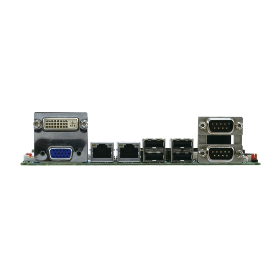
EPIC-HD07 supports 18/24-bit dual/single channel LVDS LCD and optional DVI function. In addition to the PCI-104 and Mini Card expansion, EPIC-HD07 also features one SATA, one mSATa for the storage and eight USB 2.0 ports, six COM ports, 16-bit Digital I/O co-lay with LPT function for flexible I/O expansion. -
Page 11: Features
E P I C B o a r d E P I C - H D 0 7 1.2 Features ® G-series™ T56N/T44R/T40R Processor ® A55E DDR3 SOGIMM 1066/1333 (T56N) Memory Up to 4 GB Gigabit Ethernet x 2 ... -
Page 12: Specifications
E P I C B o a r d E P I C - H D 0 7 1.3 Specifications System Form Factor EPIC Board ® Processor G-series™ T56N/T44R/T40R Processor System Memory SODIMM DDR3 1066/1333 Up to ®... - Page 13 E P I C B o a r d E P I C - H D 0 7 Operation Temperature 32°F ~ 140°F (0°C ~ 60°C) Storage Temperature -40°F ~ 176°F (-40°C ~ 80°C) Operation Humidity 0% ~ 90% relative humidity, non-condensing Display: Supports CRT/LCD/DVI simultaneous/ dual view displays...
- Page 14 E P I C B o a r d E P I C - H D 0 7 Audio Line-in, Line-out, & Mic-in Touch Screen Supports 4/5-wire resistive touch screen (optional) 1- 6 Chapter 1 General Information...
-
Page 15: Chapter 2 Quick Installation Guide
E P I C B o a r d E P I C - H D 0 7 Chapter Quick Installation Guide Chapter 2 Quick Installation Guide... -
Page 16: Safety Precautions
E P I C B o a r d E P I C - H D 0 7 2.1 Safety Precautions Always completely disconnect the power cord from your board whenever you are working on it. Do not make connections while the power is on, because a sudden rush of power can damage sensitive electronic components. -
Page 17: Location Of Connectors And Jumpers
E P I C B o a r d E P I C - H D 0 7 2.2 Location of Connectors and Jumpers Component Side Component Side Chapter 2 Quick Installation Guide... - Page 18 E P I C B o a r d E P I C - H D 0 7 Solder Side Chapter 2 Quick Installation Guide...
-
Page 19: Mechanical Drawing
E P I C B o a r d E P I C - H D 0 7 2.3 Mechanical Drawing Component Side Component Side Chapter 2 Quick Installation Guide... - Page 20 E P I C B o a r d E P I C - H D 0 7 Solder Side Chapter 2 Quick Installation Guide...
- Page 21 E P I C B o a r d E P I C - H D 0 7 Heatsink 3 .0 3 .0 * 3 .0 Thermal Block and Pad Chapter 2 Quick Installation Guide...
-
Page 22: List Of Jumpers
E P I C B o a r d E P I C - H D 0 7 2.4 List of Jumpers The board has a number of jumpers that allow you to configure your system to suit your application. The table below shows the function of each of the board's jumpers: Label Function... -
Page 23: List Of Connectors
E P I C B o a r d E P I C - H D 0 7 2.5 List of Connectors The board has a number of connectors that allow you to configure your system to suit your application. The table below shows the function of each board's connectors: Label Function... - Page 24 E P I C B o a r d E P I C - H D 0 7 USB3 USB Connector USB4 USB Connector USB5 USB Connector USB6 USB Connector COM1 (Dual Port 1) COM1 RS-232 Serial Port Connector COM2 (Dual Port 2) COM2 RS-232/422/485 Serial Port Connector COM3 COM3 RS-232 Serial Port Connector...
-
Page 25: Setting Jumpers
E P I C B o a r d E P I C - H D 0 7 2.6 Setting Jumpers You configure your card to match the needs of your application by setting jumpers. A jumper is the simplest kind of electric switch. It consists of two metal pins and a small metal clip (often protected by a plastic cover) that slides over the pins to connect them. -
Page 26: At/Atx Selection (Jp1)
E P I C B o a r d E P I C - H D 0 7 2.7 AT/ATX Selection (JP1) Function OFF (Default) 2.8 COM2 Ring/+5V/+12V Selection (JP2) +12V RI2# Function +12V RI2#_SEL (Default) 2.9 2 LVDS External Backlight Control (JP3) 1 2 3 1 2 3 Backlight down... -
Page 27: Lcd Panel Voltage Selection (Jp4)
E P I C B o a r d E P I C - H D 0 7 2.10 LCD Panel Voltage Selection (JP4) LVDS1 Function +3.3V (Default) LVDS2 +3.3V Function +3.3V (Default) 2.11 LCD Backlight Control Selection (JP5) LVDS1 Voltage-mode PWM-mode 2-13... -
Page 28: Lcd Backlight Voltage Selection (Jp6)
E P I C B o a r d E P I C - H D 0 7 Function Voltage Mode PWM Mode(Default) LVDS2 Voltage-mode PWM-mode Function Voltage Mode PWM Mode(Default) 2.12 LCD Backlight Voltage Selection (JP6) LVDS1 +12V Function +12V (Default) LVDS2 +12V... -
Page 29: Clear Cmos (Jp7)
E P I C B o a r d E P I C - H D 0 7 Function +12V (Default) 2.13 Clear CMOS (JP7) 1 2 3 1 2 3 Normal Clear CMOS Function Protected (Default) Clear 2.14 DDR3/DDR3L Voltage Control (JP8) DDR3 DDR3L Function... -
Page 30: Touch Screen Connector Selection (Jp10)
E P I C B o a r d E P I C - H D 0 7 Function +3.3V (Default) 2.16 Touch Screen Connector Selection (JP10) 5-Wire 4-Wire JP10 Function 4-Wire (Default) 5-Wire 2.17 LVDS Connector (CN1) Pin Name Signal Type Signal Level LVDS_BKLEN... - Page 31 E P I C B o a r d E P I C - H D 0 7 +3.3V/ LCD_PWR LVDS_TXL0# LVDS_TXL0 LVDS_TXL1# LVDS_TXL1 LVDS_TXL2# LVDS_TXL2 LVDS_TXL3# LVDS_TXL3 LVDS_DDCPDATA +3.3V LVDS_DDCPCLK +3.3V +3.3V/ LCD_PWR 2-17 Chapter 2 Quick Installation Guide...
-
Page 32: Lvds Connector (Cn2)
E P I C B o a r d E P I C - H D 0 7 2.18 LVDS Connector (CN2) Pin Name Signal Type Signal Level LVDS_BKLEN LVDS_BKLCTL +3.3V/ LCD_PWR LVDS_TXLCLK# LVDS_TXLCLK +3.3V/ LCD_PWR LVDS_TXL0# LVDS_TXL0 LVDS_TXL1# LVDS_TXL1 LVDS_TXL2# LVDS_TXL2 LVDS_TXL3#... -
Page 33: Lpc Connector (Cn3)
E P I C B o a r d E P I C - H D 0 7 LVDS_DDCPCLK +3.3V LVDS_TXU0# OUT - LVDS_TXU0 OUT - LVDS_TXU1# OUT - LVDS_TXU1 OUT - LVDS_TXU2# OUT - LVDS_TXU2 OUT - LVDS_TXU3# OUT - LVDS_TXU3 OUT - +3.3V/... - Page 34 E P I C B o a r d E P I C - H D 0 7 Pin Name Signal Type Signal Level LAD0 LAD1 LAD2 LAD3 +3.3V +3.3V LFRAME# LPC_RST# LPC_CLK33 LDRQ#0 LDRQ#1 SERIRQ DIO Mode (DIO co-lay with LPT) Pin Name Signal type Signal Level...
- Page 35 E P I C B o a r d E P I C - H D 0 7 GPIO4 GPIO5 GPIO6 GPIO7 GPIO6 GPIO10 GPIO9 GPIO8 Pin Name Pin Number Access Address GPIO0 GPIO1 GPIO2 GPIO3 GPIO4 2-21 Chapter 2 Quick Installation Guide...
-
Page 36: 1St Backlight Connector (Cn4)
E P I C B o a r d E P I C - H D 0 7 GPIO5 GPIO6 GPIO7 GPIO8 GPIO9 GPIO10 GPIO11 GPIO12 GPIO13 GPIO14 GPIO15 2.20 1st Backlight Connector (CN4) Pin Name Signal Type Signal Level LVDS Backlight PWR LVDS Backlight control LVDS Backlight Enable... -
Page 37: 2Nd Backlight Connector (Cn5)
E P I C B o a r d E P I C - H D 0 7 2.21 2nd Backlight Connector (CN5) Pin Name Signal Type Signal Level LVDS Backlight PWR LVDS Backlight control LVDS Backlight Enable 2.22 SATA Power Connector (CN6) Pin Name Signal Type Signal Level... -
Page 38: Audio Connector (Cn7)
E P I C B o a r d E P I C - H D 0 7 2.23 Audio Connector (CN7) Pin Name Signal Type Signal Level MIC_L MIC_R GND_AUDIO LINEIN_L LINEIN_R GND_AUDIO LINEOUT_L GND_AUDIO LINEOUT_R +5V_AUDIO 2-24 Chapter 2 Quick Installation Guide... -
Page 39: Touch Screen Connector (Cn8)
E P I C B o a r d E P I C - H D 0 7 2.24 Touch Screen Connector (CN8) Pin Name Signal Type Signal Level Top Excite Bottom Excite Left Excite Right Excite Top Sense Bottom Sense Left Sense Right Sense 2.25 2-Pin Power Connector (CN9) -
Page 40: Pci-104 Connector (Cn10)
E P I C B o a r d E P I C - H D 0 7 Pin Name Signal Type Signal Level +12V +12V 2.26 PCI-104 Connector (CN10) 2-26 Chapter 2 Quick Installation Guide... -
Page 41: Atx 4-Pin Power Connector (Cn11)
E P I C B o a r d E P I C - H D 0 7 2.27 ATX 4-Pin Power Connector (CN11) Pin Name Signal Type Signal Level +12V +12V +12V +12V 2.28 Fan Connector (CN12) Pin Name Signal Type Signal Level Fan Power Control... -
Page 42: Pci-Express Mini Card Connector (Cn14)
E P I C B o a r d E P I C - H D 0 7 Pin Name Signal Type Signal Level Power Button(+) Power Button(-) External Buzzer(+) External Buzzer(-) IDE LED(+) IDE LED(-) Power LED(+) Power LED(-) Reset Switch(+) Reset Switch(-) 2.30 PCI-Express Mini Card Connector (CN14) - Page 43 E P I C B o a r d E P I C - H D 0 7 1.5V 1.5V PCIE_CLKREQ# Reserved Reserved PCIE_MINI1_100M# Reserved PCIE_MINI1_100M Reserved Reserved Reserved Reserved Reserved MINI_CARD_EN MINI_RST# MINI_CARD1_RXN DIFF MINI1_3.3V MINI_CARD1_RXP DIFF 1.5V 1.5V 2-29 Chapter 2 Quick Installation Guide...
- Page 44 E P I C B o a r d E P I C - H D 0 7 SMB_CLK MINI_CARD1_TXN DIFF SMB_DATA MINI_CARD1_TXP DIFF USBN2 DIFF USBP2 DIFF MINI1_3.3V 3.3V MINI1_3.3V 3.3V Reserved Reserved VENDOR Reserved Reserved 1.5V 1.5V DA/DSS PRESENT DETECTION MINI1_3.3V 3.3V...
-
Page 45: Msata Mini Card Connector (Cn15)
E P I C B o a r d E P I C - H D 0 7 2.31 mSATA Mini Card Connector (CN15) Pin Name Signal Type Signal Level PCIE_WAKE_UP# MINI2_3.3V 3.3V Reserved Reserved 1.5V 1.5V PCIE_CLKREQ# Reserved Reserved PCIE_MINI2_100M# Reserved PCIE_MINI2_100M... - Page 46 E P I C B o a r d E P I C - H D 0 7 Reserved Reserved Reserved MINI_CARD_EN MINI_RST# SATA_RX1_P DIFF MINI2_3.3V SATA_RX1_N DIFF 1.5V 1.5V SMB_CLK SATA_TX1_N DIFF SMB_DATA SATA_TX1_P DIFF USBN6 DIFF USBP6 DIFF MINI2_3.3V 3.3V 2-32...
-
Page 47: Dual Usb Connector (Usb1)
E P I C B o a r d E P I C - H D 0 7 MINI2_3.3V 3.3V Reserved Reserved Reserved Reserved Reserved 1.5V 1.5V Reserved Reserved MINI2_3.3V 3.3V 2.32 Dual USB Connector (USB1) Pin Name Signal Type Signal Level +5VSB USBD1-... -
Page 48: Dual Usb Connector (Usb2)
E P I C B o a r d E P I C - H D 0 7 +5VSB USBD2- USBD2+ 2.33 Dual USB Connector (USB2) Pin Name Signal Type Signal Level +5VSB USBD3- USBD3+ USBD4- USBD4+ 2-34 Chapter 2 Quick Installation Guide... -
Page 49: Usb Connector (Usb5)
E P I C B o a r d E P I C - H D 0 7 2.34 USB Connector (USB5) Pin Name Signal Type Signal Level +5VSB USBD5- USBD5+ 2.35 USB Connector (USB6) Pin Name Signal Type Signal Level +5VSB USBD6- USBD6+... -
Page 50: Usb Connector (Usb7)
E P I C B o a r d E P I C - H D 0 7 2.36 USB Connector (USB7) Pin Name Signal Type Signal Level +5VSB USBD7- USBD7+ 2.37 USB Connector (USB8) Pin Name Signal Type Signal Level +5VSB USBD8- USBD8+... -
Page 51: Rs-232 Serial Port Dual Connector (Com)
E P I C B o a r d E P I C - H D 0 7 2.38 RS-232 Serial Port Dual Connector (COM1) Pin Name Signal Type Signal Level DCD#1 RXD#1 TXD1 DTR#1 DSR#1 RTS#1 CTS#1 RI#1 DCD#2 (485D-)(422TXD-) RXD2(422RXD+) TXD2 (485D+)(422TXD+) -
Page 52: Rs-232 Serial Port Connector (Com3)
E P I C B o a r d E P I C - H D 0 7 RTS#2 CTS#2 RI#2 2.39 RS-232 Serial Port Connector (COM3) Pin Name Signal Type Signal Level DCD#3 DSR#3 RXD3 RTS#3 TXD3 CTS#3 DTR#3 RI#3 2-38 Chapter 2 Quick Installation Guide... -
Page 53: Rs-232 Serial Port Connector (Com4)
E P I C B o a r d E P I C - H D 0 7 2.40 RS-232 Serial Port Connector (COM4) Pin Name Signal Type Signal Level DCD#4 DSR#4 RXD4 RTS#4 TXD4 CTS#4 DTR#4 RI#4 2.41 RS-232 Serial Port Connector (COM5) 2-39 Chapter 2 Quick Installation Guide... -
Page 54: Rs-232 Serial Port Connector (Com6)
E P I C B o a r d E P I C - H D 0 7 Pin Name Signal Type Signal Level DCD#5 DSR#5 RXD5 RTS#5 TXD5 CTS#5 DTR#5 RI#5 2.42 RS-232 Serial Port Connector (COM6) Pin Name Signal Type Signal Level DCD#6... -
Page 55: Lpt Port Connector (Lpt1)
E P I C B o a r d E P I C - H D 0 7 CTS#6 DTR#6 RI#6 2.43 LPT Port Connector (LPT1) Pin Name Signal Type Signal Level #STROBE #AFD DATA0 #ERROR DATA1 #INIT DATA2 #SLIN DATA3 DATA4 2-41... -
Page 56: Battery Connector (Bt1)
E P I C B o a r d E P I C - H D 0 7 DATA5 DATA6 DATA7 #ACK BUSY SELECT 2.44 Battery Connector (BT1) Pin Name Signal Type Signal Level RTCBAT 2-42 Chapter 2 Quick Installation Guide... -
Page 57: Ps/2 Keyboard And Mouse Connector (Kb1)
E P I C B o a r d E P I C - H D 0 7 2.45 PS/2 Keyboard and Mouse Connector (KB1) Pin Name Signal Type Signal Level KBDATA KBCLK MSDATA MSCLK 2.46 LAN Ethernet RJ-45 Connector (LAN1) ACT/LINK SPEED Pin Name... -
Page 58: Lan Ethernet Rj-45 Connector (Lan2)
E P I C B o a r d E P I C - H D 0 7 LAN1_MDIN2 DIFF. LAN1_MDIP3 DIFF. LAN1_MDIN3 DIFF. 2.47 LAN Ethernet RJ-45 Connector (LAN2) ACT/LINK SPEED Pin Name Signal Type Signal Level LAN2_MDIP0 DIFF. LAN2_MDIN0 DIFF. - Page 59 E P I C B o a r d E P I C - H D 0 7 Pin Name Signal Type Signal Level GREEN BLUE VGA_5V CRT_PLUG DDC_SDA HSYNC VSYNC DDC_SCL Pin Name Signal Type Signal Level DVI_TX2_N DVI_TX2_P DVI_TX2_P 2-45 Chapter 2 Quick Installation Guide...
- Page 60 E P I C B o a r d E P I C - H D 0 7 DVI_AUXP DVI_AUXP DVI_AUXN VSYNC VSYNC DVI_TX1_P DVI_TX1_N DVI_TX1_N VGA_5V VGA_5V DVI_HPD DVI_HPD DVI_TX0_N DVI_TX0_P DVI_TX0_P DVI_CLK_P DVI_CLK_N DVI_CLK_N GREEN GREEN BLUE HSYNC HSYNC 2-46 Chapter 2 Quick Installation Guide...
-
Page 61: Sata Connector (Sata1)
E P I C B o a r d E P I C - H D 0 7 2.49 SATA Connector (SATA1) Pin Name Signal Type Signal Level SATA_TX0_P DIFF SATA_TX0_N DIFF SATA_RX0_N DIFF SATA_RX0_P DIFF 2-47 Chapter 2 Quick Installation Guide... - Page 62 E P I C B o a r d E P I C - H D 0 7 Below Table for China RoHS Requirements 产品中有毒有害物质或元素名称及含量 AAEON Main Board/ Daughter Board/ Backplane 有毒有害物质或元素 部件名称 铅 汞 镉 六价铬 多溴联苯 多溴二苯醚 (Pb)
-
Page 63: Chapter 3 Ami Bios Setup
E P I C B o a r d E P I C - H D 0 7 Chapter BIOS Setup Chapter 3 AMI BIOS Setup 3-1... -
Page 64: System Test And Initialization
3. The CMOS memory has lost power and the configuration information has been erased. The EPIC-HD07 CMOS memory has an integral lithium battery backup for data retention. However, you will need to replace the complete unit when it finally runs down. -
Page 65: Ami Bios Setup
E P I C B o a r d E P I C - H D 0 7 3.2 AMI BIOS Setup AMI BIOS ROM has a built-in Setup program that allows users to modify the basic system configuration. This type of information is stored in battery-backed CMOS RAM so that it retains the Setup information when the power is turned off. - Page 66 E P I C B o a r d E P I C - H D 0 7 Advanced Advanced BIOS Features Setup including TPM, ACPI, etc. Chipset Host bridge parameters. Chapter 3 AMI BIOS Setup 3-4...
- Page 67 E P I C B o a r d E P I C - H D 0 7 Boot Enables/disable quiet boot option. Security Set setup administrator password. Chapter 3 AMI BIOS Setup 3-5...
- Page 68 E P I C B o a r d E P I C - H D 0 7 Save&Exit Exit system setup after saving the changes. Chapter 3 AMI BIOS Setup 3-6...
-
Page 69: Chapter 4 Driver Installation
E P I C B o a r d E P I C - H D 0 7 Chapter Driver Installation 4 - 1 Chapter 4 Driver Installation... - Page 70 E P I C B o a r d E P I C - H D 0 7 The EPIC-HD07 comes with a DVD-ROM that contains all drivers and utilities that meet your needs. Follow the sequence below to install the drivers: Step 1 –...
- Page 71 E P I C B o a r d E P I C - H D 0 7 4.1 Installation: Insert the EPIC-HD07 DVD-ROM into the DVD-ROM Drive. And install the drivers from Step 1 to Step 5 in order. Step 1 – Install Chipset Driver 1.
- Page 72 E P I C B o a r d E P I C - H D 0 7 Step 4 – Install AHCI Driver Please refer to the Appendix D AHCI Setting Step 5 – Install Touch Driver 1. Click on the STEP5-TOUCH folder and double click on the Setup.exe 2.
-
Page 73: Appendix A Programming The Watchdog Timer
E P I C B o a r d E P I C - H D 0 7 Appendix Programming the Watchdog Timer Appendix A Programming the Watchdog Timer A-1... -
Page 74: Programming
E P I C B o a r d E P I C - H D 0 7 A.1 Programming EPIC-HD07 utilizes FINTEK 81866 chipset as its watchdog timer controller. Below are the procedures to complete its configuration and the AAEON initial watchdog timer program is also attached based on which you can develop customized program to fit your application. - Page 75 E P I C B o a r d E P I C - H D 0 7 There are three steps to complete the configuration setup: (1) Enter the MB PnP Mode; (2) Modify the data of configuration registers; (3) Exit the MB PnP Mode.
- Page 76 E P I C B o a r d E P I C - H D 0 7 Watch Dog Timer 1, 2, 3 Control Register (Index=F5h,F6h,FAh Default=00h) Appendix A Programming the Watchdog Timer A-4...
-
Page 77: F81866 Watchdog Timer Initial Program
E P I C B o a r d E P I C - H D 0 7 A.2 F81866 Watchdog Timer Initial Program Main (){ aaeonSuperIOOpen(); aaeonWdtSetCountMode(BOOL bMinute); // Set wdt count mode aaeonWdtSetTimeoutCount(BYTE tTimeout); // Set wdt timer aaeonWdtSetEnable(BOOL bEnable); // Enable wdt aaeonSuperIOClose(); } Void aaeonSuperIOOpen(){ // Config F81866 Entry key aaeonioWritePortByte(F81866_INDEX, 0x87); aaeonioWritePortByte(F81866_INDEX, 0x87); } ... - Page 78 E P I C B o a r d E P I C - H D 0 7 Void aaeonWdtSetTimeoutCount(BYTE tTimeout){ f81866SetLdn(0x07); f81866WriteByte(F81866_WDT_TIME_REG, tTimeout); } Void aaeonWdtSetEnable(BOOL bEnable){ f81866SetLdn(0x07); if(bEnable){ f81866WriteByte(0x30, 0x01); WDT_BASE_ADDR = (f81866ReadByte(F81866_WDT_BASEADDR_REG_MSB) << 8) | f81866ReadByte(F81866_WDT_BASEADDR_REG_LSB); ...
- Page 79 E P I C B o a r d E P I C - H D 0 7 Void aaeonSuperIOClose(){ aaeonioWritePortByte(F81866_INDEX, 0xaa); } Appendix A Programming the Watchdog Timer A-7...
-
Page 80: Appendix B I/O Information
E P I C B o a r d E P I C - H D 0 7 Appendix I/O Information Appendix B I/O Information... -
Page 81: I/O Address Map
E P I C B o a r d E P I C - H D 0 7 B.1 I/O Address Map Appendix B I/O Information... - Page 82 E P I C B o a r d E P I C - H D 0 7 Appendix B I/O Information...
-
Page 83: St Mb Memory Address Map
E P I C B o a r d E P I C - H D 0 7 B.2 1 MB Memory Address Map Appendix B I/O Information... -
Page 84: Irq Mapping Chart
E P I C B o a r d E P I C - H D 0 7 B.3 IRQ Mapping Chart Appendix B I/O Information... - Page 85 E P I C B o a r d E P I C - H D 0 7 Appendix B I/O Information...
-
Page 86: Dma Channel Assignments
E P I C B o a r d E P I C - H D 0 7 B.4 DMA Channel Assignments Appendix B I/O Information... -
Page 87: Appendix C Mating Connector
E P I C B o a r d E P I C - H D 0 7 Appendix Mating Connector C - 1 Appendix C Mating Connector... -
Page 88: List Of Mating Connectors And Cables
E P I C B o a r d E P I C - H D 0 7 C.1 List of Mating Connectors and Cables The table notes mating connectors and available cables. Connector Function Mating Connector Available Cable P/N Label Cable Vendor... - Page 89 E P I C B o a r d E P I C - H D 0 7 PANEL FOXCONN AS0B226-S68K CN14 MINICARD -7 F FOXCONN AS0B226-S68K CN15 mSATA -7 F ASTRON 1860044-006-R N/A DVI+VGA3 DVI/VGA RT7-17FAAM1 LAN1/LAN2 LAN TECHBEST KS-002D-ANB( USB1/2 2.0)-L CATCH...
- Page 90 E P I C B o a r d E P I C - H D 0 7 A ppendix AHCI Setting Appendix D AHCI Setting...
-
Page 91: D.1 Setting Ahci
E P I C B o a r d E P I C - H D 0 7 D.1 Setting AHCI OS installation to setup AHCI Mode. Step 1: Copy the files below from “Driver DVD -> STEP4- AHCI\WinXP\SB8xx_RAID_XP_3.2.1540.92” to Disk Step 2: Connect the USB Floppy to the board (The board on the photo is just for reference) Appendix D AHCI Setting... - Page 92 E P I C B o a r d E P I C - H D 0 7 Step 3: Setup OS Step 4: Press “F6” Appendix D AHCI Setting...
- Page 93 E P I C B o a r d E P I C - H D 0 7 Step 5: Choose “S” tep 6: Choose “AMD (R) A55E Chipset” Appendix D AHCI Setting...
- Page 94 E P I C B o a r d E P I C - H D 0 7 Step 7: It will show the model number you select and then press “ENTER Step 8: Setup is loading files Appendix D AHCI Setting...
- Page 95 E P I C B o a r d E P I C - H D 0 7 Appendix Electrical Spec ificatio for I/O Ports Appendix E Electrical Specifications for I/O Ports...
-
Page 96: E.1 Electrical Specifications For I/O Ports
E P I C B o a r d E P I C - H D 0 7 E.1 Electrical Specifications for I/O Ports Reference Signal Name Rate Output +3.3V/1A or LVDS Port 1 +5V/1A +3.3V/1A or LVDS Port 2 +5V/1A LPC Port +3.3V... - Page 97 E P I C B o a r d E P I C - H D 0 7 VGA: +5V VGA / DVI Ports DVI+VGA +5V/0.5A DVI : +5V Appendix E Electrical Specifications for I/O Ports...
Need help?
Do you have a question about the EPIC-HD07 and is the answer not in the manual?
Questions and answers