Table of Contents
Advertisement
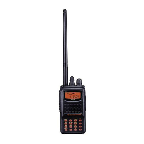
Air Band Transceiver
VXA-210
Service Manual
©
2002 VERTEX STANDARD CO., LTD. Printed in Japan.
The Vertex Standard VXA-210 Pilot is a compact, stylish, solid hand-held transceiver providing communication (transmit
and receive) capability on the International Aircraft Communication Band ("COM" band: 118 ~ 136.975 MHz), and it addi-
tionally provides VOR and CDI navigation features on the "NAV" band (108 ~ 117.975 MHz).
The VXA-210 includes Temperature display with our exclusive Omni-Glow
tion of your night vision, NOAA weather band monitoring, 8-character Alpha/Numeric Display, 50 Memory Channels, and
100 "Book Memory" Channels. And the optional Barometric Pressure Unit (SU-1) provides readout of barometric pressure,
altitude, and density altitude.
The following pages describe the Controls & Connectors, Accessories & Options, and Specification of the VXA-210.
With proper care and operation, the transceiver will provide many years of reliable communications.
Operating Manual Reprint ...................................2
Specifications ..........................................................6
Installation of the SU-1 ..........................................7
CE41 Programming Software ...............................8
Exploded View & Miscellaneous Parts ..............9
Block Diagram .......................................................10
Circuit Description ...............................................11
EC016N95A
1
2
3
4
5
6
7
8
9
MW
0
F
Contents
Alignment ............................................................. 13
Board Unit (Schematics, Layouts & Parts) ...... 17
Main Unit ......................................................... 17
Contact Unit ..................................................... 31
VR Unit ............................................................. 32
SW Unit ............................................................ 33
VERTEX STANDARD CO., LTD.
4-8-8 Nakameguro, Meguro-Ku, Tokyo 153-8644, Japan
VERTEX STANDARD
US Headquarters
17210 Edwards Rd., Cerritos, CA 90703, U.S.A.
International Division
8350 N.W. 52nd Terrace, Suite 201, Miami, FL 33166, U.S.A.
YAESU EUROPE B.V.
P.O. Box 75525, 1118 ZN Schiphol, The Netherlands
YAESU UK LTD.
Unit 12, Sun Valley Business Park, Winnall Close
Winchester, Hampshire, SO23 0LB, U.K.
VERTEX STANDARD HK LTD.
Unit 5, 20/F., Seaview Centre, 139-141 Hoi Bun Road,
Kwun Tong, Kowloon, Hong Kong
TM
display back-light for minimal degrada-
1
Advertisement
Table of Contents

Related Manuals for Vertex Standard VXA-210


Summary of Contents for Vertex Standard VXA-210
-
Page 1: Table Of Contents
100 “Book Memory” Channels. And the optional Barometric Pressure Unit (SU-1) provides readout of barometric pressure, altitude, and density altitude. The following pages describe the Controls & Connectors, Accessories & Options, and Specification of the VXA-210. With proper care and operation, the transceiver will provide many years of reliable communications. -
Page 2: Operating Manual Reprint
Operating Manual Reprint (Partial) & C ONTROLS ONNECTORS Antenna Jack This SMA jack accepts the supplied flexible antenna, or another antenna designed to provide 50 W imped- ance on the Aircraft Communication Band. POWER/VOLUME Knob Turn this control clockwise to turn the radio on and to increase the volume. -
Page 3: Operating Manual Reprint
Operating Manual Reprint (Partial) LCD D ISPLAY This field displays the course This is the Course Deviation Indicator, used heading in degrees. during VOR Navigation. This icon indicates that This indicator confirms the “Book” Memory Bank that Secondary Key Func- is in use. -
Page 4: Monitor Switch
Press this button again to the Vertex Standard Amateur or Vertex Standard Com- resume normal (quiet) monitoring. mercial radios will not work with the VXA-210. LAMP Switch EXT DC Jack Press this switch momentarily to activate the back- When an external 12-Volt DC power source is avail- lighting lamp for the display. - Page 5 Antenna Adapter (SMA to BNC) Availability of accessories may vary. Some accessories are supplied as standard per local requirements, while others may be unavailable in some regions. Consult your Vertex Standard Dealer for details regarding these and any newly-available options.
-
Page 6: Specifications
Specifications General Frequency Range: TX: 118.000 - 136.975 MHz, RX: 108.000 - 136.975 MHz, Weather Channels (WX-01 - WX-10: USA version only) Channel Spacing: 25 kHz Emission Type: TX: AM, RX: AM & FM (FM: for receiving the Weather Channels, USA version only) Supply Voltage: 6.0 - 15.0 VDC Current Consumption (approx.): 10 µA (power off), 30 mA (battery saver on, saver ratio 1:5) -
Page 7: Installation Of The Su-1
Altimeter devices used for navigation SU-1 from the transceiver. We recommend that this critical to personal safety. Rubber Cushion be put on the bottom of the SU-1. VERTEX STANDARD CO., LTD. VERTEX STANDARD CO., LTD. VERTEX STANDARD CO., LTD. VERTEX STANDARD CO., LTD. -
Page 8: Ce41 Programming Software
Do not work directly with the CE41 programming diskette. Make a copy of it and use the copy when programming the VXA-210. Keep it and the original distribution diskette in a safe place in case you need to make another copy of it later. -
Page 9: Exploded View & Miscellaneous Parts
Exploded View & Miscellaneous Parts RA0389200 WINDOW RA0321900 RUBBER CAP RA0389400 RA0111400 FRONT CASE ASSY RING NUT RA0111500 SPECIAL NUT RA0322000 RUBBER (PTT) RA0325300 RA0210600 KNOB (DIAL) RUBBER PACKING M4090142A RA0325200 RA032090A SPEAKER VOL KNOB LCD HOLDER • G6090133 RA0322100 RUBBER KNOB (16KEY) RA0324700 INTER CONNECTOR (LCD) -
Page 10: Block Diagram
Block Diagram... -
Page 11: Circuit Description
Circuit Description Receive Signal Path The processed audio signal from Q1028 passes Incoming RF from the antenna jack is passed through through the audio mute gate Q1016 (DTC124TU) and the volume control to the audio power amplifier Q1009 a low-pass filter and high-pass filter consisting of coils L1023, L1024, L1025, L1039, L1030 &... -
Page 12: Transmit Inhibit
Circuit Description Automatic Transmit Power Control reference. The 5 kHz signal from the programmable di- RF power output from the final amplifier is sampled vider (derived from the VCO) and that derived from the by C1265/C1271 and is rectified by D1039 (HSM88WA). reference oscillator are applied to the phase detector sec- The resulting DC voltage passes through the Automatic tion of Q1031, which produces a pulsed output with pulse... -
Page 13: Alignment
20 ~ 30° C (68 ~ 86° F). When the transceiver is brought VERTEX STANDARD reserves the right to change into the shop from hot or cold air, it should be allowed circuits and alignment procedures, in the interest of im- some time to come to room temperature before alignment. - Page 14 Alignment PLL Reference Frequency VOR Phase Adjustment r Connect the wattmeter, dummy load and frequency r Set the transceiver to 108.000 MHz, set up the “FROM” mode (press [ F ] + [ 3 ( FROM )] key, if necessary), and counter connected to the antenna jack, and tune the transceiver to 120.000 MHz.
- Page 15 Alignment Internal System Alignment Routine Squelch “Tight” Adjustment (TISQ) r Increase the RF signal level to +15 dBµ (5.6 µV), then This feature uses a programmed routine in the trans- press the DIAL selector knob twice. ceiver which replaces many previously-complex discrete r Now rotate the DIAL selector knob to select the next component settings and adjustments with digitally-con- trolled settings via the DIAL selector knob.
- Page 16 Note...
-
Page 17: Board Unit (Schematics, Layouts & Parts)
Main Unit Circuit Diagram 3.2V (1.1V) (0V) (1.1V) (1.6V) 6.9V 1.3V 0.9V 3.0V (6.4V) (1.8V) 6.9V (1.3V) (0.9V) (3.1V) 1.8V (6.5V) 1.8V (2.1V) (1.8V) 3.7V (1.8V) (3.7V) 0.7V 2.6V (1.3V) 3.4V (2.6V) (1.4V) (1.8V) 3.2V (0.1V) 1.9V (1.9V) (1.9V) (0.3V) 1.1V (4.0V) 1.8V... - Page 18 Main Unit Note...
- Page 19 Main Unit Parts Layout LC87F72C8A (Q1014) TK10931VT1 (Q1052) NJM2902V (Q1005) S-80745SN 2SK2974 (Q1061) (Q1027) TC7S66FU S-81235SGUP (Q1015) (Q1034) Side A AN6123MS DTA143EU (23) DTC124TU (05) DTC143ZUA (123) T1N241M (N2) UMG2N (G2) UMW1 (W1) UMZ2N (Z2) 2SA1602A (MF) 2SC4116GR (LG) MC2848 (A6) MC2850 (A7) HMS88WA (Q1008)
- Page 20 Main Unit Parts Layout 2SK880GR (XG) 02CZ2.0X (2.0X) (Q1032) (D1001) 2SK2973 (K1) MC2848 (A6) (Q1051) (D1027) 2SC3356 (R24) DAN222 (N) (Q1047) (D1004) 2SC4116GR (LG) MC2850 (A7) (Q1007, 1012, 1013, (D1008, 1028, 1037) 1040, 1045, 1050) RN739F (5F) 2SC5226 (R22) (D1038) (Q1025, 1030, 1039, 1066, 1067, 1068) 2SB1132 (BA)
-
Page 21: Parts List
Main Unit Parts List DESCRIPTION VALUE TOL. MFR'S DESIG VXSTD P/N VERS. LOT SIDE LAY ADR PCB with Compornents (with VR Unit) CS1740001 Printed Circuit Board FR0066601 C 1001 CHIP CAP. 0.001uF GRM36B102K50PT K22178809 C 1002 CHIP CAP. 0.001uF GRM36B102K50PT K22178809 C 1003 CHIP CAP. - Page 22 Main Unit Parts List DESCRIPTION VALUE TOL. MFR'S DESIG VXSTD P/N VERS. LOT SIDE LAY ADR C 1084 CHIP CAP. 0.022uF GRM36B223K16PT K22128806 C 1085 CHIP CAP. 0.022uF GRM36B223K16PT K22128806 C 1086 CHIP CAP. 10pF GRM36CH100D50PT K22178212 C 1087 CHIP CAP. 0.001uF GRM36B102K50PT K22178809...
- Page 23 Main Unit Parts List DESCRIPTION VALUE TOL. MFR'S DESIG VXSTD P/N VERS. LOT SIDE LAY ADR C 1167 CHIP CAP. 0.1uF GRM36B104K10PT K22108802 C 1169 CHIP CAP. 39pF GRM36CH390J50PT K22178226 C 1170 CHIP CAP. 0.1uF GRM36B104K10PT K22108802 C 1171 CHIP CAP. 15pF GRM36CH150J50PT K22178216...
- Page 24 Main Unit Parts List DESCRIPTION VALUE TOL. MFR'S DESIG VXSTD P/N VERS. LOT SIDE LAY ADR C 1250 CHIP CAP. 0.001uF GRM36B102K50PT K22178809 C 1251 CHIP CAP. 0.01uF GRM36B103K16PT K22128804 C 1252 CHIP TA.CAP. 2.2uF TEMSVA1C225M-8R K78120015 C 1253 CHIP CAP. 0.001uF GRM36B102K50PT K22178809...
- Page 25 Main Unit Parts List DESCRIPTION VALUE TOL. MFR'S DESIG VXSTD P/N VERS. LOT SIDE LAY ADR D 1028 DIODE MC2850-T11-1 G2070704 D 1029 DIODE HVU350TRF G2070380 D 1031 DIODE HVU350TRF G2070380 D 1032 DIODE HVU350TRF G2070380 D 1033 DIODE BAS316 G2070716 D 1034 DIODE...
- Page 26 Main Unit Parts List DESCRIPTION VALUE TOL. MFR'S DESIG VXSTD P/N VERS. LOT SIDE LAY ADR Q 1017 BU4094BCFV-E1 G1092128 Q 1018 TRANSISTOR 2SC4116GR TE85R G3341167G Q 1019 TRANSISTOR DTA143EU T106 G3070110 Q 1020 TRANSISTOR DTA143EU T106 G3070110 Q 1021 TRANSISTOR RT1N241M-T11-1 G3070249...
- Page 27 Main Unit Parts List DESCRIPTION VALUE TOL. MFR'S DESIG VXSTD P/N VERS. LOT SIDE LAY ADR R 1024 CHIP RES. 1/16W RMC1/16S 180JTH J24189004 R 1025 CHIP RES. 1/16W RMC1/16S 103JTH J24189037 R 1026 CHIP RES. 1/16W RMC1/16S 473JTH J24189045 R 1027 CHIP RES.
- Page 28 Main Unit Parts List DESCRIPTION VALUE TOL. MFR'S DESIG VXSTD P/N VERS. LOT SIDE LAY ADR R 1105 CHIP RES. 1/16W RMC1/16S 333JTH J24189043 R 1106 CHIP RES. 1/16W RMC1/16S 473JTH J24189045 R 1107 CHIP RES. 220k 1/16W RMC1/16S 224JTH J24189053 R 1108 CHIP RES.
- Page 29 Main Unit Parts List DESCRIPTION VALUE TOL. MFR'S DESIG VXSTD P/N VERS. LOT SIDE LAY ADR R 1185 CHIP RES. 4.7k 1/16W RMC1/16S 472JTH J24189033 R 1186 CHIP RES. 1/10W RMC1/10T 470J J24205470 R 1187 CHIP RES. 470k 1/16W RMC1/16S 474JTH J24189057 R 1188 CHIP RES.
- Page 30 Main Unit Parts List DESCRIPTION VALUE TOL. MFR'S DESIG VXSTD P/N VERS. LOT SIDE LAY ADR R 1269 CHIP RES. 1/16W RMC1/16S 103JTH J24189037 TC1001 TRIMMER CAP. 20pF CTZ2S-20C-W2-P K91000216 TH1001 THERMISTOR TBPS1R473K475H5Q G9090068 TH1003 THERMISTOR TBPS1R223K460H5Q G9090085 TH1004 THERMISTOR ERTJ0ET102J G9090131 VR1001 POT.
-
Page 31: Contact Unit
Contact Unit Circuit Diagram 6.9V 3.0V (6.6V) (3.0V) Parts Layout S-81230SG (QB) Side A Side B (Q4001) Parts List DESCRIPTION VALUE TOL. MFR'S DESIG VXSTD P/N VERS. LOT SIDE LAY ADR PCB with Components CB1485001 Printed Cirsuit Board FR0069700 C 4001 CHIP CAP. -
Page 32: Vr Unit
VR Unit Circuit Diagram 3.5V 3.0V (0V) (3.5V) 5.0V (5.0V) 3.6V (3.2V) (3.5V) Parts Layout UMG2N (G2) (Q2001) 12-22SURSYGC/ S530-A2/TR8 Side A Side B (D2001) Parts List DESCRIPTION VALUE TOL. MFR'S DESIG VXSTD P/N VERS. LOT SIDE LAY ADR PCB with Comporments CB1483001 Printed Circuit Board FR006680A... -
Page 33: Sw Unit
SW Unit Parts Layout Parts Layout Side A Side B Parts List DESCRIPTION VALUE TOL. MFR'S DESIG VXSTD P/N VERS. LOT SIDE LAY ADR PCB with Components CB1484001 Printed Circuit Board FR002650B S 3001 TACT SWITCH SOP-114HST R66-5374 N5090107 S 3002 TACT SWITCH SOP-114HST R66-5374 N5090107... - Page 34 Copyright 2002 VERTEX STANDARD CO., LTD. All rights reserved. No portion of this manual may be reproduced without the permission of VERTEX STANDARD CO., LTD. Printed in Japan...
Need help?
Do you have a question about the VXA-210 and is the answer not in the manual?
Questions and answers