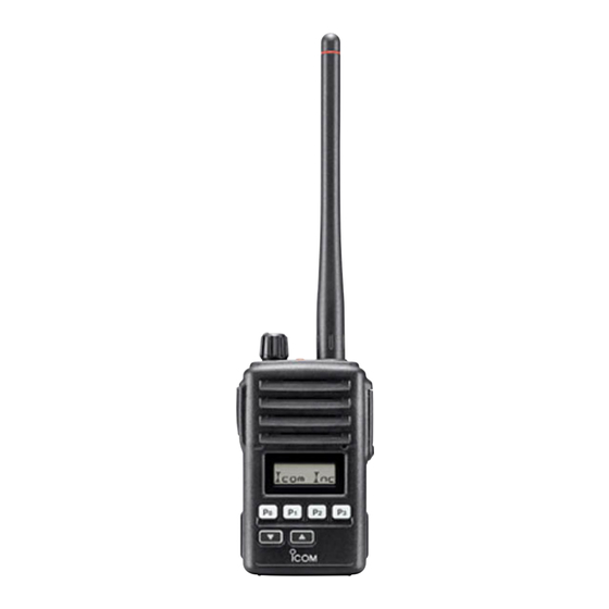
Icom IC-F50 Service Manual
Vhf transceiver
Hide thumbs
Also See for IC-F50:
- Insrtuction manual (64 pages) ,
- Instruction manual (64 pages) ,
- Service manual addendum (57 pages)
Table of Contents
Advertisement
Advertisement
Chapters
Table of Contents

Subscribe to Our Youtube Channel
Related Manuals for Icom IC-F50


Summary of Contents for Icom IC-F50
- Page 1 SERVICE MANUAL VHF TRANSCEIVER...
- Page 2 INTRODUCTION This service manual describes the latest service information for the IC-F50/IC-F51 VHF TRANSCEIVER at the time of publication. MODEL VERSION SYMBOL U.S.A IC-F50 General Europe IC-F51 To upgrade quality, all electrical or mechanical parts and internal circuits are subject to change without notice or oblig- ation.
-
Page 3: Table Of Contents
VR / CONNECTOR BOARDS ..........11-3 Icom, Icom Inc. and are registered trademarks of Icom Incorporated (Japan) in the United States, the United Kingdom, Germany, France, Spain, ussia and/or other countries. -
Page 4: Specifications
SECTION 1 SPECIFICATIONS ‘ ‘ GENERAL • Frequency coverage : 136.000–174.000 MHz • Mode : FM • Type of emission VERSION WIDE MIDDLE NARROW 11K0F3E (12.5 kHz) [USA], [GEN] 16K0F3E (25.0 kHz) [EUR] 14K0F3E (20.0 kHz) 8K0F3E (12.5 kHz) • Number of conventional channels : 128 ch, 8banks : SMA type (50 Ω) •... -
Page 5: Section 2 Inside Views
SECTION 2 INSIDE VIEWS • MAIN UNIT TOP VIEW BOTTOM VIEW +5 Regurator Antenna (IC9: NJM2870) switching circuit S5 Regulator (D2,D5: 1SV307) Q23: 2SB1132 Power amplifier Q24: XP6501 (Q7: RD07MVS1) Q25: DTA144EU TX/RX APC amplifier T5 Regulator switch (IC2: TA75S01F) (Q21: 2SA1577) (D14,D15: MA2S077) VCO circuit... -
Page 6: Section 3 Disassembly Instructions
SECTION 3 DISASSEMBLY INSTRUCTIONS • • REMOVING THE FRONT UNIT REMOVING THE CHASSIS UNIT 1 Unscrew 4 screws M. 1 Unscrew 1 nut A, and remove 1 knob B. 2 Remove 1 washer c, and unscrew 1 screw D. 2 Unsolder 11 points N. 3 Unplug the connector O from J402 on the Front unit. -
Page 7: Receiver Circuits
SECTION 4 CIRCUIT DESCRIPTION 4-1 RECEIVER CIRCUITS The RF signals from the bandpass filter are mixed with the 1st LO signals, where come from the RX VCO circuit via the 4-1-1 ANTENNA SWITCHING CIRCUIT attenuator (R26–R28), at the 1st mixer circuit (Q3) to pro- (MAIN UNIT) duce a 46.35 MHz 1st IF signal. -
Page 8: Transmitter Circuits
4-1-5 AF AMPLIFIER CIRCUIT • CTCSS AND DTCS The tone squelch circuit detects AF signals and opens the (MAIN AND FRONT UNITS) squelch only when receiving a signal containing a matching The AF amplifier circuit amplifies the demodulated AF sig- subaudible tone (CTCSS or DTCS). - Page 9 4-2-2 MODULATION CIRCUIT (MAIN UNIT) The power detector circuit (D1) detects the transmit power output level and converts it into DC voltage. The output volt- The modulation circuit modulates the VCO oscillating signal age is at a minimum level when the antenna impedance is (RF signal) using the microphone audio signals.
- Page 10 4-4-2 FRONT UNIT VOLTAGE LINE 4-3-2 VCO CIRCUIT (MAIN UNIT) The VCO circuit contains a separate RX VCO (Q14, D19, LINE DESCRIPTION D20) and TX VCO (Q13, D16, D17). The oscillated signal is Same voltage as VCC line on the MAIN unit is amplified at the buffer amplifiers (Q10, Q12) and is then applied to the FRONT unit via the J401, pins 1, applied to the T/R switch (D14, D15).
-
Page 11: Other Circuits
4-6 PORT ALLOCATIONS 4-5 OTHER CIRCUITS 4-6-1 EXPANDER IC (FRONT UNIT; IC410) 4-5-1 COMPOUNDER CIRCUIT (MAIN UNIT) IC-F50/F51 have compounder circuit which can improve S/N Port Description ratio and become wide dynamic range to suppress the number name transmitting signal and to extend receiving signal. The circuit Outputs RX LED control signal. - Page 12 4-6-2 MAIN CPU (FRONT unit; IC401) Port Port Description Description number name number name 1–11, SEG23– Input port for the PTT switch detection SEG13, signal. Output segment data to the LCD dis- Low: While switch SEG12, play. pushed. 15–25, SEG11– Input ports for the key return A/D sig- SEG1 nals.
- Page 13 4-6-3 EXPANDER IC (FRONT UNIT; IC410) 4-6-5 EXPANDER IC (MAIN UNIT; IC12) Port Port Description Description number name number name Outputs RX LED control signal. Outputs the R5 regulator (Q22) control LEDR Low: Lights ON. signal. Low: While receiving. Outputs TX LED control signal. LEDT Low: Lights ON.
-
Page 14: Section 5 Adjustment Procedures
SECTION 5 ADJUSTMENT PROCEDURES 5-1 PREPARATION When adjusting IC-F60/F61, the optional CS-F50 ADJ (Rev. 1.0 or later), *OPC-966 (modified ADJUSTMENT SOFTWARE JIG CABLE OPC-966 ) are required. CLONING CABLE I REQUIRED TEST EQUIPMENT EQUIPMENT GRADE AND RANGE EQUIPMENT GRADE AND RANGE Output voltage : 7.5 V DC Frequency range... - Page 15 • SCREEN DISPLAY EXAMPLE CS-F50 ADJ Rev.1.0 File Option COM 1: OPEN Connect Reload (F5) Disp para [A / D] [D / A] : 203 : CBh : 7.96 V BPF T1 : 108 : 6Ch : 2.12 V TEMPS : 190 : BEh : 32.23 'C T2/POW : 103 : 67h : 2.02 V LVIN...
- Page 16 SSG is connected to 0.1–10 W/50 Ω the antenna connector Frequency counter Personal computer to an RS-232C port IC-F50/F51 Audio generator DB9 female plug SINAD meter (incl. level converter circuit) *OPC-966 RS-232C cable (straight) (JIG CABLE) Speaker (8 Ω) •...
- Page 17 5-2 SOFTWARE ADJUSTMENTS (TRANSMITTING) Select an operation using [↑] / [↓] keys, then set specified value using [←] / [→] keys on the connected computer keyboard. MEASUREMENT ADJUSTMENT ADJUSTMENT CONDITION VALUE UNIT LOCATION PLL LOCK • Operating CH : CH3 Soft Check the “LV”...
-
Page 18: Software Adjustments
SOFTWARE ADJUSTMENTS (RECEIVING) • Select an operation using [↑] / [↓] keys, then set specified value using [←] / [→] keys on the connected computer keyboard. • Need to adjust “S-METER ADJUSTMENT” after “RX SENSITIVITY ADJUSTMENT” is adjusted. Otherwise, “S-METER ADJUSTMENT” will not be adjusted properly. MEASUREMENT ADJUSTMENT ADJUSTMENT CONDITION... -
Page 19: Section 6 Parts List
SECTION 6 PARTS LIST [VR BOARD] [FRONT UNIT] ORDER ORDER DESCRIPTION DESCRIPTION R601 7210003130 VARIABLE TP76N97N-13F-10KA-2497 X401 6050011720 S.XTAL CR-764 (19.6608 MHz) W601 8900012340 CABLE OPC-1260 R401 7030005220 S.RESISTOR ERJ2GEJ 223 X (22 kΩ) R402 7030005060 S.RESISTOR ERJ2GEJ 333 X (33 kΩ) R403 7030005120 S.RESISTOR... - Page 20 [FRONT UNIT] [FRONT UNIT] ORDER ORDER DESCRIPTION DESCRIPTION R494 7030008010 S.RESISTOR ERJ2GEJ 123 X (12 kΩ) C490 4030017460 S.CERAMIC ECJ0EB1E102K R495 7030008010 S.RESISTOR ERJ2GEJ 123 X (12 kΩ) C491 4030017460 S.CERAMIC ECJ0EB1E102K R496 7030005050 S.RESISTOR ERJ2GEJ 103 X (10 kΩ) C492 4030017460 S.CERAMIC...
- Page 21 [MAIN UNIT] [MAIN UNIT] ORDER ORDER DESCRIPTION DESCRIPTION 1520000450 S.TRANSISTOR 2SB1132 T100 Q 7030005030 S.RESISTOR ERJ2GEJ 152 X (1.5 kΩ) 1590001190 S.TRANSISTOR XP6501-(TX) .AB 7030005090 S.RESISTOR ERJ2GEJ 104 X (100 kΩ) ERJ2GEJ 100 X (10 Ω) 1590000720 S.TRANSISTOR DTA144EUA T106 7030005530 S.RESISTOR 1590003320...
- Page 22 [MAIN UNIT] [MAIN UNIT] ORDER ORDER DESCRIPTION DESCRIPTION R113 7030005040 S.RESISTOR ERJ2GEJ 472 X (4.7 kΩ) 4030017580 S.CERAMIC ECJ0EC1H060C R115 7030007570 S.RESISTOR ERJ2GEJ 122X (1.2 kΩ) 4030017430 S.CERAMIC ECJ0EC1H101J R116 7030007060 S.RESISTOR ERJ2GEJ 684X (680 kΩ) 4030017460 S.CERAMIC ECJ0EB1E102K R117 7030005040 S.RESISTOR ERJ2GEJ 472 X (4.7 kΩ)
- Page 23 [MAIN UNIT] [MAIN UNIT] ORDER ORDER DESCRIPTION DESCRIPTION C117 4030017730 S.CERAMIC ECJ0EB1E471K C235 4030016790 S.CERAMIC ECJ0EB1C103K C118 4030017530 S.CERAMIC ECJ0EC1H0R5B C236 4510004630 S.ELECTROLYTIC ECEV1CA100SR C119 4030017460 S.CERAMIC ECJ0EB1E102K C237 4030016790 S.CERAMIC ECJ0EB1C103K C120 4030017730 S.CERAMIC ECJ0EB1E471K C238 4550005980 S.TANTALUM TEESVA 1A 475M8L C121 4030017390 S.CERAMIC...
-
Page 24: Mechanical Parts And Disassembly
SECTION 7 MECHANICAL PARTS AND DISASSEMBLY 7-1 CABINET PARTS [MAIN UNIT] [ACCESSORIES] REF. NO. ORDER NO. DESCRIPTION QTY. REF. NO. ORDER NO. DESCRIPTION QTY. 8510015670 2681 shield plate 0800006730 Battery BP-227 3310003020 Antenna FA-S59V ACC [CHASSIS PARTS] 8930061480 Clip MB-98 ACC 8210017071 2337 C-PANEL-1 REF. - Page 25 Unit:mm (inch) CONNECTOR BOARD MP419 ( F ) MP6 ( C ) FRONT Unit R601 ( V ) MP9 ( C ) MP424 ( F ) MP8 ( C ) 56 (2 MP407 ( F ) J1 ( C ) 31.4 (2 62.5 (4 MP421 ( F )
- Page 26 SECTION 8 SEMI-CONDUCTOR INFORMATION • TRANSISTOR AND FET’S 2SA1577 Q 2SB1132 Q 2SC4116 BL 2SC4116 Y 2SC4215 O (Symbol: HP) (Symbol: BAQ) (Symbol: LL) (Symbol: LY) (Symbol: QO) 2SC4226 R25 2SC5107 O 2SC5110 O 2SK880 Y 2SK1829 (Symbol: R25) (Symbol: MFO) (Symbol: MGO) (Symbol: XY) (Symbol: K1)
-
Page 27: Section 9 Board Layouts
SECTION 9 BOARD LAYOUTS 9-1 MAIN UNIT • TOP VIEW J1 (CHASSIS UNIT) R168 R167 C295 C230 C106 C186 R171 R172 to the FRONT unit J401 C141 C104 R100 C139 C111 R101 C143 R173 R174 C147 C146 C206 C203 C201 C202 PWON C145... -
Page 28: Bottom View
• BOTTOM VIEW C292 R165 C233 C238 C308 C101 C231 R161 C182 C102 R169 C183 C122 C118 C113 C135 C115 C114 C117 C116 C192 C190 C194 C191 C127 C129 C133 C134 C149 R164 C232 C151 C152 R117 C240 C155 C153 R118 C132 C154... -
Page 29: Front Unit
9-2 FRONT UNIT • TOP VIEW S401 J402 to the VR board W601 DUSE AFOUT R435 SIGNAL PWON J402 R436 C436 R514 C429 C450 R479 R480 C449 C427 C447 Q401 J401 R478 C448 to the MAIN unit J1 C488 C443 C441 IC406 R437... - Page 30 • BOTTOM VIEW Q405 Q404 R443 C426 R445 C484 C433 MC401 R457 DS402 DS403 9 - 4...
-
Page 31: Vr Board
9-3 VR BOARD • TOP VIEW R601 • BOTTOM VIEW VHF B6034B 9 - 5... -
Page 32: Connector Board
9-4 CONNECTOR BOARD • TOP VIEW RESET MICE OPTV D704 • BOTTOM VIEW OPTV C704 D705 C703 C702 C701 D703 D702 D701 9 - 6... -
Page 33: Block Diagram
SECTION 10 BLOCK DIAGRAM 136–174MHz Q17: Q15: XP1214 Q18: 2SK880 2SC4116 Q16: DTC144EU Q14: 2SC4226 D19,20: HVC376B LVIN RIPPLE BUFF MAIN UNIT D22: HVC375B RX VCO IC16: CR–763 Q12: D2: 1SV307 Q10: D14,D15: 15.3 MHz 2SC5107 2SC5110 RD01MUS1 RD07MVS1 RB706F D5: 1SV307 NJM12904 2SC5107... -
Page 34: Voltage Diagram
SECTION 11 VOLTAGE DIAGRAM 11-1 MAIN UNIT R98 2.2 k 1.8 k 3.9 k 15.3MHz 2SC4116BL VCOM 1.2Vp–p 2SC4226R25 EXCCL3225V C127 C126 47 P 68 nH 33 P 10 k R103 470 k ERJ2GE–JPW 3.3 H C211 R102 2SK880Y 0.001 47 k C102 (CHASSIS) - Page 35 11-2 FRONT UNIT R488 100 k C408 C409 C410 C411 CPU5 R489 100 k CPU5 R420 R421 R422 R423 R490 100 k 27 k 100 k 100 k 100 k Beat Cancel OFF 19.6618MHz OPTV CPU5 2.7Vp–p SEG23 SENC0 PM6/SEG31 P70/TMRI01/TMCI01 C413 SEG22...
-
Page 36: Vr / Connector Boards
11-3 VR / CONNECTOR BOARDS VR BOARD R601 TP76N97N-13F-10KA-2497 DUSE AFOUT From / to the J402 SIGNAL at the FRONT UNIT PWON W601 CONNECTOR BOARD EP701 EP702 OPTV EP703 MICE R701 OPTV MICE OPTV To the FRONT UNIT RESET RESET MP701 EP704 EP705... - Page 38 S-14007IZ-C1 1-1-32, Kamiminami, Hirano-ku, Osaka, 547-0003, Japan © 2003 Icom Inc.
- Page 39 SERVICE MANUAL UHF TRANSCEIVER...
- Page 40 INTRODUCTION This service manual describes the latest service information for the IC-F60/IC-F61 UHF TRANSCEIVER at the time of publication. FREQUENCY MODEL VERSION SYMBOL USA-02 U.S.A USA-08 USA-88 400-470 MHz GEN-02 General GEN-08 IC-F60 USA-03 USA-09 U.S.A 450-512 MHz USA-89 GEN-03 General GEN-09 EUR-02...
- Page 41 VR / CONNECTOR BOARDS ..........11-3 Icom, Icom Inc. and are registered trademarks of Icom Incorporated (Japan) in the United States, the United Kingdom, Germany, France, Spain, ussia and/or other countries.
- Page 42 SECTION 1 SPECIFICATIONS ‘ ‘ GENERAL • Frequency coverage : 400.000–470.000 MHz [USA], [EUR], [GEN] 450.000–512.000 MHz [USA] 450.000–520.000 MHz [GEN] • Mode : FM • Type of emission VERSION WIDE MIDDLE NARROW 11K0F3E (12.5 kHz) [USA], [GEN] 16K0F3E (25.0 kHz) [EUR] 14K0F3E (20.0 kHz) 8K0F3E (12.5 kHz)
- Page 43 SECTION 2 INSIDE VIEWS • MAIN UNIT TOP VIEW BOTTOM VIEW Antenna +5 Regurator switching circuit (IC9: NJM2870) D2: 1SV307 S5 Regulator D5:MA2S077 Q23: 2SB1132 Q Q24: XP6501 AB Power amplifier Q25: DTA144EU (Q7: RD07MVS1) TX/RX T5 Regulator APC amplifier switch (Q21: 2SA1577 Q) (IC2: TC75S51F)
-
Page 44: Section 3 Disassembly Instructions
SECTION 3 DISASSEMBLY INSTRUCTIONS • • REMOVING THE FRONT UNIT REMOVING THE CHASSIS UNIT 1 Unscrew 4 screws M. 1 Unscrew 1 nut A, and remove 1 knob B. 2 Remove 1 washer c, and unscrew 1 screw D. 2 Unsolder 11 points N. 3 Unplug the connector O from J402 on the Front unit. -
Page 45: Receiver Circuits
SECTION 4 CIRCUIT DESCRIPTION 4-1 RECEIVER CIRCUITS mixer. The RF signals from the bandpass filter are mixed with the 4-1-1 ANTENNA SWITCHING CIRCUIT 1st LO signals, where come from the RX VCO circuit via the (MAIN UNIT) low-pass filter (L38, C363, C364), at the 1st mixer circuit The antenna switching circuit functions as a low-pass filter (Q3) to produce a 46.35 MHz 1st IF signal. -
Page 46: Transmitter Circuits
4-1-5 AF AMPLIFIER CIRCUIT • CTCSS AND DTCS The tone squelch circuit detects AF signals and opens the (MAIN AND FRONT UNITS) squelch only when receiving a signal containing a matching The AF amplifier circuit amplifies the demodulated AF sig- subaudible tone (CTCSS or DTCS). -
Page 47: Pll Circuits
The filtered AF signals are applied to the FM/PM switch 4-2-4 APC CIRCUIT (MAIN UNIT) (MAIN unit; IC11, pin 6), and pass through the low-pass fil- The APC circuit (IC2, D1, D39) protects the drive and power ter (MAIN unit; IC5, pin 1). The amplified signals are applied amplifiers from excessive current drive, and selects output to the D/A converter (MAIN unit;... -
Page 48: Power Supply Circuits
4-4 POWER SUPPLY CIRCUIT 4-3-2 VCO CIRCUIT (MAIN UNIT) The VCO circuit contains a separate RX VCO (Q13, D16) 4-4-1 MAIN UNIT VOLTAGE LINE and TX VCO (Q14, D17). The oscillated signal is amplified LINE DESCRIPTION at the buffer amplifiers (Q10, Q11) and is then applied to the T/R switch (D14, D15). -
Page 49: Other Circuits
4-6 PORT ALLOCATIONS 4-5 OTHER CIRCUITS 4-6-1 EXPANDER IC (FRONT UNIT; IC410) 4-5-1 COMPOUNDER CIRCUIT (MAIN UNIT) IC-F60/F61 have compounder circuit which can improve S/N Port Description ratio and become wide dynamic range to suppress the number name transmitting signal and to extend receiving signal. The circuit Outputs RX LED control signal. - Page 50 4-6-2 CPU (FRONT unit; IC401) Port Port Description Description number name number name SEG23– Input port for the PTT switch detection 1–11, SEG13, signal. Output segment data to the LCD dis- SEG12, Low: While switch play. 15–25, SEG11– pushed. SEG1 Input ports for the key return A/D sig- Outputs serial data to the PLL IC nals.
- Page 51 4-6-3 EXPANDER IC (FRONT UNIT; IC410) 4-6-5 EXPANDER IC (MAIN UNIT; IC12) Port Port Description Description number name number name Outputs RX LED control signal. Outputs the R5 regulator (Q22) control LEDR Low: Lights ON. signal. Low: While receiving. Outputs TX LED control signal. LEDT Low: Lights ON.
-
Page 52: Section 5 Adjustment Procedures
SECTION 5 ADJUSTMENT PROCEDURES 5-1 PREPARATION When adjusting IC-F60/F61, the optional CS-F50 ADJ (Rev. 1.0 or later), *OPC-966 (modified ADJUSTMENT SOFTWARE JIG CABLE OPC-966 ) are required. CLONING CABLE I REQUIRED TEST EQUIPMENT EQUIPMENT GRADE AND RANGE EQUIPMENT GRADE AND RANGE Output voltage : 7.5 V DC Frequency range... - Page 53 • SCREEN DISPLAY EXAMPLE CS-F50 ADJ Rev.1.0 File Option COM 1: OPEN Connect Reload (F5) Disp para [A / D] [D / A] : 203 : CBh : 7.96 V BPF T1 : 108 : 6Ch : 2.12 V TEMPS : 190 : BEh : 32.23 'C T2/POW : 103 : 67h : 2.02 V LVIN...
- Page 54 • CONNECTION Standard signal generator to the antenna connector 0.1 µV to 32 mV (–127 dBm to –17 dBm) Attenuator deviation meter 40 dB or 50 dB CAUTION! DO NOT transmit while RF power meter to SSG is connected to 0.1–10 W/50 Ω...
- Page 55 5-2 SOFTWARE ADJUSTMENT (TRANSMITTING) Select an operation using [↑] / [↓] keys, then set specified value using [←] / [→] keys on the connected computer keyboard. MEASUREMENT ADJUSTMENT ADJUSTMENT CONDITION VALUE UNIT LOCATION PLL LOCK • Operating CH : CH3 MAIN Check the “LV”...
- Page 56 SOFTWARE ADJUSTMENT(TRANSMITTING) – continued Select an operation using [↑] / [↓] keys, then set specified value using [←] / [→] keys on the connected computer keyboard. MEASUREMENT ADJUSTMENT ADJUSTMENT CONDITION VALUE UNIT LOCATION MODULATION • Operating CH : CH7 Connect an FM deviation Set to square wave BALANCE •...
- Page 57 SOFTWARE ADJUSTMENT (RECEIVING) • Select an operation using [↑] / [↓] keys, then set specified value using [←] / [→] keys on the connected computer keyboard. • Need to adjust “S-METER ADJUSTMENT” after “RX SENSITIVITY ADJUSTMENT” is adjusted. Otherwise, “S-METER ADJUSTMENT” will not be adjusted properly. MEASUREMENT ADJUSTMENT ADJUSTMENT CONDITION...
-
Page 58: Section 6 Parts List
SECTION 6 PARTS LIST [FRONT UNIT] [FRONT UNIT] ORDER ORDER DESCRIPTION DESCRIPTION IC401 1140011780 S.IC HD6432264F01TF (FX-2681A) R462 7030005720 S.RESISTOR ERJ2GEJ 563 X (56 kΩ) IC403 1110005340 S.IC NJM12902V-TE1 R463 7030005220 S.RESISTOR ERJ2GEJ 223 X (22 kΩ) IC405 1110001810 S.IC TA7368F (ER) R464 7030005220... - Page 59 [FRONT UNIT] [MAIN UNIT] ORDER ORDER DESCRIPTION DESCRIPTION C434 4550006250 S.TANTALUM TEESVA 1A 106M8L 1110003200 S.IC TA31136FN (EL) C435 4550007060 S.TANTALUM ECSTIAX336R 1130008560 S.IC TC75S51F (TE85L) C436 4030016950 S.CERAMIC ECJ0EB1A473K 1140005990 S.IC MB15A02PFV1-G-BND-ER C437 4030017490 S.CERAMIC C1608 JB 1A 105K-T 1110005340 S.IC NJM12902V-TE1...
- Page 60 [MAIN UNIT] [MAIN UNIT] ORDER ORDER DESCRIPTION DESCRIPTION 6200007680 S.COIL LQW2BHN12NJ01L 7030005050 S.RESISTOR ERJ2GEJ 103 X (10 kΩ) 7030005040 S.RESISTOR ERJ2GEJ 472 X (4.7 kΩ) 6200007230 S.COIL LQW2BHN15NJ01L ERJ2GEJ 100 X (10 Ω) 7030005530 S.RESISTOR 6200007680 S.COIL LQW2BHN12NJ01L 7030005240 S.RESISTOR ERJ2GEJ 473 X (47 kΩ) 6200005720 S.COIL...
- Page 61 [MAIN UNIT] [MAIN UNIT] ORDER ORDER DESCRIPTION DESCRIPTION R170 7030005170 S.RESISTOR ERJ2GEJ 474 X (470 kΩ) 4030017400 S.CERAMIC ECJ0EC1H220J R173 7030008400 S.RESISTOR ERJ2GEJ 182 X (1.8 kΩ) 4030017460 S.CERAMIC ECJ0EB1E102K R180 7030005120 S.RESISTOR ERJ2GEJ 102 X (1 kΩ) 4030017460 S.CERAMIC ECJ0EB1E102K R181 7030005220...
- Page 62 [MAIN UNIT] [MAIN UNIT] ORDER ORDER DESCRIPTION DESCRIPTION A only C143 4030017460 S.CERAMIC ECJ0EB1E102K C277 4030017490 S.CERAMIC C1608 JB 1A 105K-T A only C144 4030017420 S.CERAMIC ECJ0EC1H470J C279 4030017650 S.CERAMIC ECJ0EC1H270J C145 4030017420 S.CERAMIC ECJ0EC1H470J A only C280 4030017650 S.CERAMIC ECJ0EC1H270J C146 4550000270...
- Page 63 [VR UNIT] ORDER DESCRIPTION R601 7210003130 VARIABLE TP76N97N-13F-10KA-2497 W601 8900012340 CABLE OPC-1260 EP601 0910056532 B 6034B [CONNECTOR UNIT] ORDER DESCRIPTION D701 1790001810 S.VARISTOR AVR-M1005C080MTABB D702 1790001810 S.VARISTOR AVR-M1005C080MTABB D703 1790001810 S.VARISTOR AVR-M1005C080MTABB D704 1790001810 S.VARISTOR AVR-M1005C080MTABB D705 1790001810 S.VARISTOR AVR-M1005C080MTABB R701 7410001130 S.ARRAY...
- Page 64 SECTION 7 MECHANICAL PARTS AND DISASSEMBLY 7-1 CABINET PARTS [MAIN UNIT] [ACCESSORIES] REF. NO. ORDER NO. DESCRIPTION QTY. REF. NO. ORDER NO. DESCRIPTION QTY. 8510016150 2682 shield plate 0800006730 Battery BP-227 MP10 8930062950 Shield sponge (AF) [EUR2], [EUR8] 3310003150 Antenna FA-S27U ACC 3310003170 Antenna FA-S56U ACC [CHASSIS PARTS] 8930061480 Clip MB-98 ACC...
- Page 65 Unit:mm (inch) NOTE: Loop the wires once, as shown, to keep it away from the speaker. MP702 (C) Doing this also keep the transmit radiation within specification. MP419 ( F ) CONNECTOR BOARD MP10 ( C ) MP6 ( C ) FRONT Unit R601 ( V ) MP9 ( C )
- Page 66 SECTION 8 SEMI-CONDUCTOR INFORMATION • TRANSISTOR AND FET’S 2SA1577 Q 2SB1132 Q 2SC3356 R25 2SC4116 BL 2SC4116 Y (Symbol: HP) (Symbol: BAQ) (Symbol: R25) (Symbol: LL) (Symbol: LY) 2SC4215 O 2SC4226 R25 2SC5107 O 2SK880 Y 2SK1829 (Symbol: QO) (Symbol: R25) (Symbol: MFO) (Symbol: XY) (Symbol: K1)
-
Page 67: Section 9 Board Layouts
SECTION 9 BOARD LAYOUTS 9-1 MAIN UNIT • TOP VIEW C237 R167 R168 R297 C239 C295 C230 C368 R371 R338 C375 to the FRONT unit J401 C339 C111 R173 C206 PWON R109 R111 C208 C145 CSFT C146 C209 DAST MRDF MDIA C223 R182... - Page 68 • BOTTOM VIEW R165 C365 C233 C235 C238 R337 C367 C291 C292 C374 R161 R235 C302 C103 C102 R169 C364 C104 C122 C148 C120 C127 C134 C133 C124 R114 C287 R164 C232 R184 C152 R117 C153 R118 C154 C240 C279 C165 R147 C166...
-
Page 69: Front Unit
9-2 FRONT UNIT • TOP VIEW S401 J402 to the VR board W601 DUSE AFOUT SIGNAL PWON R435 J402 R436 C436 R514 C429 C450 R479 R480 C449 C427 C447 Q401 J401 R478 to the MAIN unit J1 C448 C488 C443 C441 IC406 R437... - Page 70 • BOTTOM VIEW Q405 Q404 C426 R445 C484 R443 C433 MC401 R457 DS402 DS403 9 - 4...
-
Page 71: Vr Board
9-3 VR BOARD • TOP VIEW R601 • BOTTOM VIEW B6034B 9 - 5... -
Page 72: Connector Board
9-4 CONNECTOR BOARD • TOP VIEW RESET MICE OPTV D704 • BOTTOM VIEW OPTV C704 D705 C703 C702 C701 D703 D702 D701 9 - 6... -
Page 73: Block Diagram
SECTION 10 BLOCK DIAGRAM 400–520MHz Q17: Q15: XP1214 Q18: 2SC4116 Q16: DTC144EU 2SK880 Q13: 2SC4226 D16: HVC350B LVIN RIPPLE BUFF MAIN UNIT D22: HVC350B RX VCO CR–763 D2: 1SV307 IC5: Q11: Q10: D14,D15: NJM12902 15.3 MHz 2SC5107 2SC5107 MA2S077 2SC5107 2SC3356 RD01MUS1 RD07MVS1... - Page 74 SECTION 11 VOLTAGE DIAGRAM 11-1 MAIN UNIT A: The scrambler IC is installed type. B: The scrambler IC is not installed type. C: High-band. D: Low-band. E: Intrinsically safe version. RX VCO 2SC4116BL 6.8 k 6.8 k C124 C123 5 P C 12 P D 1.8 H 10 P D...
- Page 75 11-2 FRONT UNIT R488 100 k C408 C409 C410 C411 CPU5 R489 100 k CPU5 R420 R421 R422 R423 R490 100 k 27 k 100 k 100 k 100 k Beat Cancel OFF 19.6618MHz OPTV CPU5 2.7Vp–p SEG23 SENC0 PM6/SEG31 P70/TMRI01/TMCI01 C413 SEG22...
-
Page 76: Vr / Connector Boards
11-3 VR / CONNECTOR BOARDS VR BOARD R601 TP76N97N-13F-10KA-2497 DUSE AFOUT From / to the J402 SIGNAL at the FRONT UNIT PWON W601 CONNECTOR BOARD EP701 EP702 OPTV EP703 MICE R701 OPTV MICE OPTV To the FRONT UNIT RESET RESET MP701 EP704 EP705... - Page 78 S-14010IZ-C1 1-1-32, Kamiminami, Hirano-ku, Osaka, 547-0003, Japan © 2004 Icom Inc.
Need help?
Do you have a question about the IC-F50 and is the answer not in the manual?
Questions and answers