Table of Contents
Advertisement
QQ
3 7 63 1515 0
SERVICE MANUAL
Ver. 1.1 2005.05
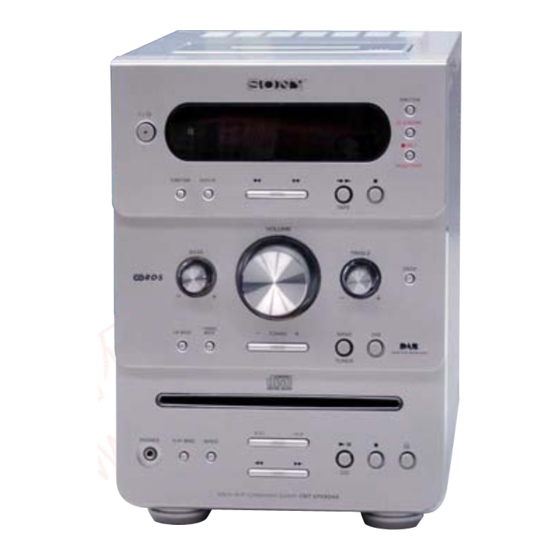
HCD-GPX9 is the amplifier, CD player, tape deck
and tuner section in CMT-GPX9DAB.
TE
L 13942296513
AUDIO POWER SPECIFICATIONS
Main unit
Amplifier section
DIN power output (rated): 30 + 30 W
Continuous RMS power output (reference):
Music power output (reference):
Inputs
AUDIO IN:
Outputs
PHONES:
SPEAKER:
CD player section
Laser Diode Properties
www
.
Sony Corporation
9-879-468-02
Personal Audio Group
2005E05-1
Published by Sony Engineering Corporation
© 2005.05
http://www.xiaoyu163.com
* This output is the value measurement at a distance of
200 mm from the objective lens surface on the
Optical Pick-up Block with 7 mm operture.
Frequency response
Wavelength
(6 ohms at 1 kHz, DIN)
Tape deck section
35 + 35 W
Recording system
(6 ohms at 1 kHz, 10%
Frequency response
THD)
60 + 60 W
Tuner section
Sensitivity 250 mV,
DAB tuner section
impedance 47 kilohms
Frequency range
Band-III:
Accepts headphones with
an impedance of 8 ohms or
L-Band:
more
Accepts impedance of 6 to
16 ohms.
* For details, see "DAB frequency table" below.
Emission Duration:
Continuous
Laser Output*:
Less than 44.6 µW
x
ao
y
i
http://www.xiaoyu163.com
HCD-GPX9
8
Model Name Using Similar Mechanism
CD Mechanism Type
CD
Section
Base Unit Name
Optical Pick-up Block Name
Model Name Using Similar Mechanism
Tape deck
Q Q
Section
Tape Transport Mechanism Type
3
6 7
1 3
SPECIFICATIONS
µ
20 Hz – 20 kHz
780 – 790 nm
4-track 2-channel, stereo
50 – 13,000 Hz (±3 dB),
using Sony TYPE I
cassettes
174.928 (5A) –
239.200 (13F) MHz
1452.960 MHz (L1) –
1490.624 MHz (L23)
(L-Band is not available
for the UK model.)
COMPACT DISC DECK RECEIVER
u163
.
2 9
9 4
2 8
AEP Model
HCD-GPX5
CDM80B-K6BD80A
BU-K6BD80A
KSM-213DCP
HCD-GPX5
CMAL1Z234A
1 5
0 5
8
2 9
9 4
Aerial terminal
FM stereo, FM/AM superheterodyne tuner
FM tuner section
Tuning range
Aerial
Aerial terminals
Intermediate frequency
AM tuner section
Tuning range
Aerial
Intermediate frequency
– Continued on next page –
m
co
9 9
UK Model
2 8
9 9
75 Ω, F female
87.5 – 108.0 MHz
FM lead aerial
75 ohms unbalanced
10.7 MHz
531 – 1,602 kHz
(with the tuning interval
set at 9 kHz)
AM loop aerial, external
aerial terminal
450 kHz
Advertisement
Table of Contents

Related Manuals for Sony HCD-GPX9


Summary of Contents for Sony HCD-GPX9
- Page 1 HCD-GPX9 3 7 63 1515 0 SERVICE MANUAL AEP Model UK Model Ver. 1.1 2005.05 HCD-GPX9 is the amplifier, CD player, tape deck and tuner section in CMT-GPX9DAB. Model Name Using Similar Mechanism HCD-GPX5 CD Mechanism Type CDM80B-K6BD80A Section...
- Page 2 COMPONENTS IDENTIFIED BY MARK 0 OR DOTTED LINE WITH MARK 0 ON THE SCHEMATIC DIAGRAMS AND IN THE PARTS LIST ARE CRITICAL TO SAFE OPERATION. REPLACE THESE COMPONENTS WITH SONY PARTS WHOSE PART NUMBERS APPEAR AS SHOWN IN THIS MANUAL OR IN SUPPLEMENTS PUBLISHED BY SONY.
-
Page 3: Table Of Contents
HCD-GPX9 3 7 63 1515 0 TABLE OF CONTENTS SERVICING NOTES EXPLODED VIEWS ..........4 7-1. Side Plates Section ............52 GENERAL 7-2. Front Panel Section ............53 7-3. Top Block Section ............54 Location of Controls ............6 7-4. -
Page 4: Servicing Notes
HCD-GPX9 SECTION 1 SERVICING NOTES 3 7 63 1515 0 UNLEADED SOLDER NOTES ON HANDLING THE OPTICAL PICK-UP Boards requiring use of unleaded solder are printed with the lead- BLOCK OR BASE UNIT free mark (LF) indicating the solder contains no lead. - Page 5 HCD-GPX9 3 7 63 1515 0 – CD Mechanism deck – CD mechanism deck L 13942296513 – AMP Board – 2 Remove the AMP board from heat sink. heat sink 1 two screws × (BVTP3 AMP board u163 heat sink...
-
Page 6: General
HCD-GPX9 SECTION 2 This section is extracted from instruction manual. GENERAL 3 7 63 1515 0 List of button locations and reference pages Main unit ALPHABETICAL ORDER BUTTON DESCRIPTIONS ?/1 (power) 1 A – O P – Z ./> (CD skip back/skip BASS +/–... -
Page 7: Setting The Clock
HCD-GPX9 3 7 63 1515 0 Remote control ALPHABETICAL ORDER BUTTON DESCRIPTIONS ?/1 (power) 1 A – O P – Z m/M (rewind/fast forward) CD qh PLAY MODE qk CLEAR qd REPEAT 4 ./> (skip back/skip CLOCK/TIMER SELECT 2 SLEEP w;... -
Page 8: Disassembly
HCD-GPX9 SECTION 3 DISASSEMBLY 3 7 63 1515 0 • This set can be disassembled in the order shown below. 3-1. DISASSEMBLY FLOW 3-2. SIDE PLATE (L)/(R) (Page 9) 3-3. TOP BLOCK ASSY (Page 9) 3-5. FRONT PANEL 3-4. TAPE MECHANISM DECK... -
Page 9: Side Plate (L)/(R)
HCD-GPX9 3 7 63 1515 0 Note: Follow the disassembly procedure in the numerical order given. 3-2. SIDE PLATE (L) / (R) 1 screw × (BVTP3 5 side plate (L) 2 two screws × (BVTT3 6 screw × (BVTP3 3 screw ×... -
Page 10: Tape Mechanism Deck (Cmal1Z234A)
HCD-GPX9 3 7 63 1515 0 3-4. TAPE MECHANISM DECK (CMAL1Z234A) 3 tape mechanism deck 2 harness (CMAL1Z234A) 1 four screws × (BVTP3 L 13942296513 3-5. FRONT PANEL SECTION 2 connector (CN604) 1 wire (flat type) (21 core) (CN310) 5 front panel section 4 Open the plate. -
Page 11: Main Board
HCD-GPX9 3 7 63 1515 0 3-6. MAIN BOARD 4 heat sink cover 3 two screws × 0 wire (flat type) (BVTT3 2 three connectors (15 core) (CN305) (CN603, 605, 901) qa wire (flat type) (11 core) (CN315) qs wire (flat type) (17 core) -
Page 12: Cd Mechanism Deck Block
HCD-GPX9 3 7 63 1515 0 3-8. CD MECHANISM DECK BLOCK 1 connector 4 DAB block 2 two screws × (KTP3 8 screw × (BVTT3 9 two screws × (BVTT3 5 screw 0 cover (CDM) × (BVTT3 6 three screws ×... -
Page 13: Bd Board
HCD-GPX9 3 7 63 1515 0 3-10. BD BOARD 4 BD board 2 wire (flat type) (16 core) (CN101) 3 screw (2.6) 1 Remove four solders. L 13942296513 3-11. DRIVER BOARD 2 two screws (BVTP 2.6) 5 DRIVER board Remove two solders. -
Page 14: Chassis (Top)
HCD-GPX9 3 7 63 1515 0 3-12. CHASSIS (TOP) 4 three screws 1 screw (BVTP 2.6) (BVTP 2.6) 3 two screws (P 2 × 10) 2 lever (CL UP2) 5 chassis (top) L 13942296513 u163 http://www.xiaoyu163.com... -
Page 15: Lever (Loading-L/R)
HCD-GPX9 3 7 63 1515 0 3-13. LEVER (LOADING-L/R) SPT-T (loading-R) SPT-T (loading-L) L 13942296513 5 lever (loading-R) 2 two hooks 4 two hooks 3 lever (loading-L) PRECAUTION DURING LEVER (LOADING R / L) INSTALLATION — Bottom view —... -
Page 16: Lever (Disc Sensor)/(Disc Stop)
HCD-GPX9 3 7 63 1515 0 3-14. LEVER (DISC SENSOR)/(DISC STOP) 1 gear (cap) 2 gear (IDL L) PRECAUTION DURING DISC STOP LEVER INSTALLATION chassis (top) hole 5 two hooks 3 two claws lever (disc stop) 6 lever (disc stop) -
Page 17: Lever (Bu Lock)
HCD-GPX9 3 7 63 1515 0 3-16. LEVER (BU LOCK) 1 floating screw (PTPWH M2.6) 5 lever (BU lock) 4 three hooks 2 gear (cap) 3 gear (BU lock) L 13942296513 3-17. CLOSE LEVER 1 washer (3-1-0.4) 5 close lever... -
Page 18: Lever (Dir), Gear (Idl-B)
HCD-GPX9 3 7 63 1515 0 3-18. LEVER (DIR), GEAR (IDL-B) 3 nylon washer 1.7 2 claw 4 pulley (gear) washer 5 gear (cap) 6 gear (IDL-A) 9 stoper 0 lever (DIR) qa gear (IDL-B) 1 DIR SPR-E 7 Loosen the screw. -
Page 19: Test Mode
HCD-GPX9 SECTION 4 TEST MODE 3 7 63 1515 0 [MC COLD RESET] [PANEL TEST MODE] Enter The Panel Test Mode The cold reset clears all data including preset data stored in the memory to initial conditions. Execute this mode when returning Procedure: the set to the customer. - Page 20 HCD-GPX9 3 7 63 1515 0 [CD REPEAT 5 LIMIT CANCEL MODE] Number of repeat for CD playback is 5 times when the repeat mode is “REPEAT”. This mode enables CD to repeat playback for limitless times. Procedure: 1. Press the button to turn the power on.
-
Page 21: Electrical Adjustments
HCD-GPX9 SECTION 5 ELECTRICAL ADJUSTMENTS 3 7 63 1515 0 DECK SECTION 1. Demagnetize the record/playback head with a head demagnetizer. 2. Do not use a magnetized screwdriver for the adjustments. 3. After the adjustments, apply suitable locking compound to the parts adjust. -
Page 22: Cd Section
HCD-GPX9 3 7 63 1515 0 CD SECTION Note: 1. CD Block is basically constructed to operate without adjustment. 2. Use YEDS-18 disc (3-702-101-01) unless otherwise indicated. 3. Use an oscilloscope with more than 10 MΩ impedance. 4. Clean the object lens by an applicator with neutral detergent when the signal level is low than specified value with the following checks. -
Page 23: Diagrams
HCD-GPX9 SECTION 6 3 7 6 3 1 5 1 5 0 DIAGRAMS 6-1. BLOCK DIAGRAM – CD SERVO Section – FILTER XTSL CD DSP XTAO IC101 (1/2) X171 CLOCK 48 50 47 49 DETECTOR XTAI CD +3V 16.9344MHz... -
Page 24: Block Diagram - Audio Section
HCD-GPX9 3 7 6 3 1 5 1 5 0 6-2. BLOCK DIAGRAM – AUDIO Section – AC DET (Page 25) HP SW (Page 25) J301 INPUT SELECT, R-CH J321 MD IN L TONE CONTROL, POWER ON PHONES ELECTRICAL VOLUME... -
Page 25: Block Diagram - Panel/Power Supply Section
HCD-GPX9 3 7 6 3 1 5 1 5 0 6-3. BLOCK DIAGRAM – PANEL/POWER SUPPLY Section – SYSTEM CONTROLLER FL/LED DRIVER IC306 (3/3) IC801 REMOTE CONTROL GR1 – GR12 RECEIVER SIRCS IN/ FL701 WAKE IC802 FLUORESCENT INDICATOR TUBE SG1 –... - Page 26 HCD-GPX9 Ver. 1.1 3 7 6 3 1 5 1 5 0 • Note for Printed Wiring Boards and Schematic Diagrams • Circuit Boards Location Note on Printed Wiring Board: Note on Schematic Diagram: • X : parts extracted from the component side.
-
Page 27: Printed Wiring Board - Driver Board
HCD-GPX9 3 7 6 3 1 5 1 5 0 6-4. PRINTED WIRING BOARD – DRIVER Board – • See page 26 for Circuit Boards Location. 6-5. SCHEMATIC DIAGRAM – DRIVER Board – • See page 44 for IC Block Diagrams. -
Page 28: Printed Wiring Board - Bd Board
HCD-GPX9 3 7 6 3 1 5 1 5 0 • See page 26 for Circuit Boards Location. 6-6. PRINTED WIRING BOARD – BD Board – : Uses unleaded solder. OPTICAL PICK-UP BLOCK (KSM-213DCP) BD BOARD C116 C123 JW118... -
Page 29: Schematic Diagram - Bd Board
HCD-GPX9 3 7 6 3 1 5 1 5 0 6-7. SCHEMATIC DIAGRAM – BD Board – • See page 44 for IC Block Diagrams. • See page 44 for Waveforms. CN201 XTACN TP29 XTACN C201 C182 C181 AGND... -
Page 30: Printed Wiring Board - Dab Board
HCD-GPX9 Ver. 1.1 3 7 6 3 1 5 1 5 0 • See page 26 for Circuit Boards Location. 6-8. PRINTED WIRING BOARD – DAB Board – : Uses unleaded solder. DAB BOARD C922 C792 C924 C791 C732... -
Page 31: Schematic Diagram - Dab Board
HCD-GPX9 Ver. 1.1 3 7 6 3 1 5 1 5 0 6-9. SCHEMATIC DIAGRAM – DAB Board – • See page 44 for IC Block Diagrams. DAB TUNER MODULE ANTENNA DAB C703 0.0047 CN700 LOW-PASS FILTER C730 C701... -
Page 32: Printed Wiring Board - Main Board
HCD-GPX9 Ver. 1.1 3 7 6 3 1 5 1 5 0 • See page 26 for Circuit Boards Location. 6-10. PRINTED WIRING BOARD – MAIN Board – : Uses unleaded solder. • Semiconductor Location TAPE MECHANISM (Page 42) Ref. -
Page 33: Schematic Diagram - Main Board (1/3)
HCD-GPX9 3 7 6 3 1 5 1 5 0 • See page 44 for Waveforms. • See page 44 for IC Block Diagram. 6-11. SCHEMATIC DIAGRAM – MAIN Section (1/3) – (1/3) CN315 R132 C132 R119 ST CLK 470p 4.7k... -
Page 34: Schematic Diagram - Main Board (2/3)
HCD-GPX9 Ver. 1.1 3 7 6 3 1 5 1 5 0 • See page 44 for Waveforms. • See page 49 for IC Pin Function Description. 6-12. SCHEMATIC DIAGRAM – MAIN Section (2/3) – (Page 33) (2/3) Q308,309... -
Page 35: Schematic Diagram - Main Board (3/3)
HCD-GPX9 6-13. SCHEMATIC DIAGRAM – MAIN Section (3/3) – 3 7 6 3 1 5 1 5 0 (Page 33) (3/3) C236 TM301 1000p CN309 R CH R GND SPEAKER RELAY - L GND IMPEDANCE RELAY + L102 USE 6 – 16Ω... -
Page 36: Printed Wiring Board - Amp Board
HCD-GPX9 • See page 26 for Circuit Boards Location. 6-14. PRINTED WIRING BOARD – AMP Board – : Uses unleaded solder. 3 7 6 3 1 5 1 5 0 • Semiconductor Location AMP BOARD Ref. No. Location D501... -
Page 37: Schematic Diagram - Amp Board
HCD-GPX9 3 7 6 3 1 5 1 5 0 • See page 44 for IC Block Diagram. 6-15. SCHEMATIC DIAGRAM – AMP Board – C609 D610 POWER AMP 1SS133T-72 IC601 STK433-040 R619 PROTECT CONTROL R626 IC602 RT8H015C-T112-1 Q608... -
Page 38: Printed Wiring Board - Panel (1) Board
HCD-GPX9 3 7 6 3 1 5 1 5 0 • See page 26 for Circuit Boards Location. 6-16. PRINTED WIRING BOARD – PANEL (1) Board – : Uses unleaded solder. • Semiconductor Location Ref. No. Location PANEL (1) BOARD... -
Page 39: Schematic Diagram - Panel (1) Board
HCD-GPX9 • See page 44 for IC Block Diagram. 6-17. SCHEMATIC DIAGRAM – PANEL (1) Board – 3 7 6 3 1 5 1 5 0 FL701 FLUORESCENT INDICATOR TUBE S801 S802 S803 ROTARY ENCODER ROTARY ENCODER ROTARY ENCODER... -
Page 40: Printed Wiring Board - Panel (2) Board
HCD-GPX9 3 7 6 3 1 5 1 5 0 • See page 26 for Circuit Boards Location. 6-18. PRINTED WIRING BOARD – PANEL (2) Board – : Uses unleaded solder. PANEL (2) BOARD S718 – 726 J321 PHONES... -
Page 41: Schematic Diagram - Panel (2) Board
HCD-GPX9 3 7 6 3 1 5 1 5 0 6-19. SCHEMATIC DIAGRAM – PANEL (2) Board – S726 R828 R827 R826 R825 R824 R823 R822 R821 4.7k 2.2k 1.5k CN803 FB221 S725 S724 S723 S722 S721 S720 S719... -
Page 42: Printed Wiring Board - Power Board
HCD-GPX9 • See page 26 for Circuit Boards Location. 3 7 6 3 1 5 1 5 0 6-20. PRINTED WIRING BOARD – POWER Board – : Uses unleaded solder. • Semiconductor Location MAIN BOARD Ref. No. Location CN307... -
Page 43: Schematic Diagram - Power Board
HCD-GPX9 3 7 6 3 1 5 1 5 0 6-21. SCHEMATIC DIAGRAM – POWER Board – D906 D908 1N4002 1N4002 D902 D904 1N4002 1N4002 +10V REGULATOR IC901 TA7810S D907 D909 1N4002 1N4002 D903 D905 1N4002 1N4002 C909 C901... -
Page 44: Http://Www.xiaoyu163.Com
HCD-GPX9 3 7 6 3 1 5 1 5 0 • Waveforms • IC Block Diagrams – DRIVER Board – – BD Board – – MAIN Board – IC701 BA6956AN IC101 w; (TEI) Q303, 304 (Collector) (CD Play Mode) -
Page 45: Http://Www.xiaoyu163.Com
HCD-GPX9 3 7 63 1515 0 – BD Board – IC101 CXD3058AR 108 107 105 104 103 102 112 111 CPU INTERFACE SERVO INTERFACE 84 RMUT 83 IOVDD0 82 AVDD2 81 AOUT2 COVERTER 80 VREFR MIRR MIRR DFCT DFCT... -
Page 46: Http://Www.xiaoyu163.Com
HCD-GPX9 3 7 63 1515 0 IC251 BA5947FM-E2 MUTING + – INTERFACE LEVEL SHIFT INTERFACE INTERFACE VREF L 13942296513 – DAB Board – IC907 BA50BC0WFP-E2 IC911 BA33BC0WFP-E2 VREF – DRIVER THERMAL OVER CURRENT SHUT DOWN PROTECT u163 http://www.xiaoyu163.com... - Page 47 HCD-GPX9 3 7 63 1515 0 – MAIN Board – IC201 HD14053BFP B.COM OPEN A.COM C.COM OPEN OPEN IC302 BD3402KS2 56 55 54 53 52 51 48 NC 47 NC 46 NC 45 NC L 13942296513 44 BNF1 43 BOUT1 −...
-
Page 48: Http://Www.xiaoyu163.Com
HCD-GPX9 3 7 63 1515 0 – AMP Board – IC602 RT8H015C-T112-1 OVER LOAD DETECT DETECT – PANEL (1) Board – IC801 µPD16315GB-3BS L 13942296513 LED1 LED2 4-BIT LATCH LED3 LED4 GRID 12-BIT SHIFT DRIVER REGISTER KEY DATA MEMORY... -
Page 49: Http://Www.xiaoyu163.Com
HCD-GPX9 Ver. 1.1 3 7 63 1515 0 • IC Pin Function Description MAIN BOARD IC306 M30622MEP-A27FPU0 (SYSTEM CONTROLLER) Pin No. Pin Name Description Not used CD DISCSENS 2 Not used CD DISCSENS 1 STBY LED LED drive signal output terminal (power) -
Page 50: Http://Www.xiaoyu163.Com
HCD-GPX9 3 7 63 1515 0 Pin No. Pin Name Description SW2-1 (CLOSE) CD close switch input terminal Not used DAB POWER 5 Power on/off control signal output for the DAB Power on/off control signal output for the DAB DAB POWER 3.3... -
Page 51: Http://Www.xiaoyu163.Com
HCD-GPX9 3 7 63 1515 0 Pin No. Pin Name Description EQ CLK Serial data transfer clock signal output to the electrical volume 89 to 91 KEY3 to KEY1 Front panel key or headphone detection input terminal (A/D input) -
Page 52: Exploded Views
HCD-GPX9 Ver. 1.1 SECTION 7 EXPLODED VIEWS 3 7 63 1515 0 NOTE: • -XX and -X mean standardized parts, so they • Items marked “*” are not stocked since they The components identified by mark 0 or dotted line with mark 0 are may have some difference from the original are seldom required for routine service. -
Page 53: Front Panel Section
HCD-GPX9 3 7 63 1515 0 7-2. FRONT PANEL SECTION panel (1) board supplied FL701 not supplied L 13942296513 supplied Ref. No. Part No. Description Remark Ref. No. Part No. Description Remark 4-251-909-01 KNOB, VOLUME 4-251-887-01 INDICATOR, POWER 4-251-910-01 KNOB, B/T... -
Page 54: Top Block Section
HCD-GPX9 3 7 63 1515 0 7-3. TOP BLOCK SECTION not supplied L 13942296513 supplied not supplied Ref. No. Part No. Description Remark Ref. No. Part No. Description Remark X-4956-091-1 HOLDER ASSY, CASSETTE 4-224-104-41 DAMPER 4-251-899-02 SPRING, CASSETTE 3-701-748-00 CLAMP... -
Page 55: Main Section
HCD-GPX9 Ver. 1.1 3 7 63 1515 0 7-4. MAIN SECTION not supplied (AEP, EE) CD mechanism deck section-1 (CDM80B-K6BD80A) supplied not supplied (UK) not supplied (AEP, EE) not supplied not supplied supplied (included 156) L 13942296513 not supplied... -
Page 56: Chassis Section-2
HCD-GPX9 Ver. 1.1 3 7 63 1515 0 7-5. CHASSIS SECTION-2 power board not supplied F901 F902 T901 not supplied L 13942296513 not supplied not supplied The components identified by mark 0 or dotted line with mark 0 are critical for safety. -
Page 57: Cd Mechanism Deck Section-1 (Cdm80B-K6Bd80A)
HCD-GPX9 3 7 63 1515 0 7-6. CD MECHANISM DECK SECTION-1 (CDM80B-K6BD80A) CD mechanism deck section-2 (CDM80B-K6BD80A) L 13942296513 BU-K6BD80A Ref. No. Part No. Description Remark Ref. No. Part No. Description Remark 2-515-538-01 SPRING (HOLDER DOWN B), COIL 4-231-151-01 STOPPER (BU) -
Page 58: Cd Mechanism Deck Section-2 (Cdm80B-K6Bd80A)
HCD-GPX9 3 7 63 1515 0 7-7. CD MECHANISM DECK SECTION-2 (CDM80B-K6BD80A) CD mechanism section-3 (CDM80B-K6BD80A) M701 L 13942296513 CD mechanism section-4 (CDM80B-K6BD80A) Ref. No. Part No. Description Remark Ref. No. Part No. Description Remark 4-245-630-01 LEVER (SW) 4-985-672-01 SCREW (+PTPWHM2.6), FLOATING 3-087-053-01 BVTP2.6 (3CR) -
Page 59: Cd Mechanism Deck Section-3 (Cdm80B-K6Bd80A)
HCD-GPX9 3 7 63 1515 0 7-8. CD MECHANISM DECK SECTION-3 (CDM80B-K6BD80A) L 13942296513 Ref. No. Part No. Description Remark Ref. No. Part No. Description Remark 4-245-627-01 WASHER (6-2.7-0.4) 4-245-640-01 GEAR (CAP) 4-245-637-01 ROLLER, RUBBER 1-452-925-21 MAGNET ASSY 4-245-649-01 GEAR (IDL-I) -
Page 60: Cd Mechanism Deck Section-4 (Cdm80B-K6Bd80A)
HCD-GPX9 3 7 63 1515 0 7-9. CD MECHANISM DECK SECTION-4 (CDM80B-K6BD80A) supplied L 13942296513 supplied Ref. No. Part No. Description Remark Ref. No. Part No. Description Remark 4-245-643-01 GEAR (IDL-C) 4-245-628-01 LEVER (BU LOCK) X-2021-531-1 CHASSIS (BOTTOM) ASSY 2-515-536-01 SPRING (DIR), TENSION COIL 4-248-206-01 WASHER (3-1-0.4) -
Page 61: Base Unit Section (Bu-K6Bd80A)
HCD-GPX9 3 7 63 1515 0 7-10. BASE UNIT SECTION (BU-K6BD80A) (including M101 (spindle), M102 (sled)) not supplied M101 (spindle) not supplied L 13942296513 M102 (sled) S101 The components identified by mark 0 or dotted line with mark 0 are critical for safety. -
Page 62: Electrical Parts List
HCD-GPX9 Ver. 1.1 SECTION 8 3 7 63 1515 0 ELECTRICAL PARTS LIST NOTE: • Due to standardization, replacements in the • Items marked “*” are not stocked since they The components identified by mark 0 or dotted line with mark 0 are parts list may be different from the parts are seldom required for routine service. - Page 63 HCD-GPX9 3 7 63 1515 0 Ref. No. Part No. Description Remark Ref. No. Part No. Description Remark R553 1-216-821-11 METAL CHIP 1/10W C125 1-164-360-11 CERAMIC CHIP 0.1uF R555 1-216-864-11 SHORT CHIP C131 1-162-927-11 CERAMIC CHIP 100PF R556 1-216-824-11 METAL CHIP 1.8K...
- Page 64 HCD-GPX9 Ver. 1.1 3 7 63 1515 0 Ref. No. Part No. Description Remark Ref. No. Part No. Description Remark JR111 1-216-296-11 SHORT CHIP C711 1-164-156-11 CERAMIC CHIP 0.1uF C712 1-164-156-11 CERAMIC CHIP 0.1uF < TRANSISTOR > C713 1-126-933-11 ELECT...
- Page 65 HCD-GPX9 Ver. 1.1 DRIVER MAIN 3 7 63 1515 0 Ref. No. Part No. Description Remark Ref. No. Part No. Description Remark R714 1-216-821-11 METAL CHIP 1/10W C115 1-126-964-11 ELECT 10uF C116 1-164-227-11 CERAMIC CHIP 0.022uF R716 1-216-797-11 METAL CHIP...
- Page 66 HCD-GPX9 Ver. 1.1 MAIN 3 7 63 1515 0 Ref. No. Part No. Description Remark Ref. No. Part No. Description Remark C307 1-130-485-00 MYLAR 0.015uF D306 8-719-991-33 DIODE 1SS133T-77 C308 1-130-481-00 MYLAR 0.0068uF 5% D307 8-719-991-33 DIODE 1SS133T-77 C309 1-130-481-00 MYLAR 0.0068uF 5%...
- Page 67 HCD-GPX9 MAIN 3 7 63 1515 0 Ref. No. Part No. Description Remark Ref. No. Part No. Description Remark < TRANSISTOR > R205 1-216-825-11 METAL CHIP 2.2K 1/10W R206 1-216-841-11 METAL CHIP 1/10W Q102 8-729-107-43 TRANSISTOR 2SC3624-L18 R207 1-216-845-11 METAL CHIP...
- Page 68 HCD-GPX9 MAIN PANEL (1) 3 7 63 1515 0 Ref. No. Part No. Description Remark Ref. No. Part No. Description Remark R350 1-249-425-11 CARBON 4.7K 1/4W R469 1-216-809-11 METAL CHIP 1/10W R358 1-216-841-11 METAL CHIP 1/10W R472 1-216-809-11 METAL CHIP...
- Page 69 HCD-GPX9 PANEL (1) PANEL (2) 3 7 63 1515 0 Ref. No. Part No. Description Remark Ref. No. Part No. Description Remark C832 1-126-964-11 ELECT 10uF R819 1-216-833-11 METAL CHIP 1/10W C833 1-107-826-11 CERAMIC CHIP 0.1uF R830 1-216-806-11 METAL CHIP...
- Page 70 HCD-GPX9 Ver. 1.1 PANEL (2) POWER 3 7 63 1515 0 Ref. No. Part No. Description Remark Ref. No. Part No. Description Remark D902 8-719-063-79 DIODE 1N4002B < RESISTOR > D903 8-719-063-79 DIODE 1N4002B D904 8-719-063-79 DIODE 1N4002B R821...
- Page 71 HCD-GPX9 3 7 63 1515 0 MEMO L 13942296513 u163 http://www.xiaoyu163.com...
- Page 72 HCD-GPX9 3 7 63 1515 0 REVISION HISTORY Clicking the version allows you to jump to the revised page. Also, clicking the version at the upper right on the revised page allows you to jump to the next revised page.
Need help?
Do you have a question about the HCD-GPX9 and is the answer not in the manual?
Questions and answers