Table of Contents
Advertisement
SERVICE MANUAL
Ver 1.0 2004.04
HCD-GPX6/GPX7 are the amplifier, CD player,
tape deck and tuner section in CMT-GPX6/GPX7.
AUDIO POWER SPECIFICATIONS
POWER OUTPUT AND TOTAL HARMONIC DISTORTION:
(The United States model only)
With 6 ohm loads, both channels driven, from
120-10,000 Hz; rated 35 watts per channel minimum
RMS power, with no more than 10% total harmonic
dist ortion from 250 milliwatts to rated output.
Amplifier section
HCD-GPX7
DIN power output (rated): 40 + 40 W (6 ohms at 1 kHz, DIN)
Continuous RMS power output (reference): 60 + 60 W
(6 ohms at 1 kHz, 10% THD)
Music power output (reference): 100 + 100 W
HCD-GPX6
North American model:
Continuous RMS power output (reference): 40 + 40 W
(6 ohms at 1 kHz, 10% THD)
Other models:
The following measured at AC 240 V, AC 220 V or AC 120 V
DIN power output (rated): 30 + 30 W (6 ohms at 1 kHz, DIN)
Continuous RMS power output (reference): 35 + 35 W
(6 ohms at 1 kHz, 10% THD)
Inputs
MD/VIDEO:
Sensitivity 450/250 mV, impedance
47 kilohms
Outputs
PHONES:
Accepts headphones with an
impedance of 8 ohms or more
SPEAKER:
Accepts impedance of 6 to 16 ohms.
Sony Corporation
9-877-742-01
2004D05-1
Home Audio Company
© 2004.04
Published by Sony Engineering Corporation
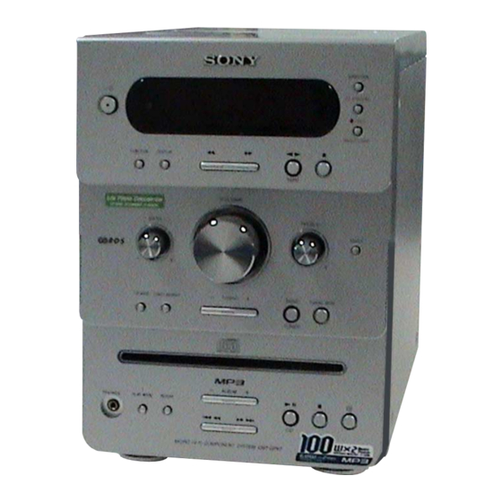
HCD-GPX6/GPX7
Photo: HCD-GPX7
CD
Section
Tape deck
Section
SPECIFICATIONS
CD player section
Laser
Semiconductor laser (λ=780 nm)
Emission duration: continuous
20 Hz − 20 kHz
Frequency response
780 − 790 nm
Wavelength
Tape deck section
Recording system
4-track 2-channel, stereo
50 − 13,000 Hz (±3 dB), using
Frequency response
Sony TYPE I cassettes
Tuner section
FM stereo, FM/AM superheterodyne tuner
FM tuner section
87.5 − 108.0 MHz
Tuning range
Antenna
FM lead antenna
Antenna terminals
75 ohms unbalanced
Intermediate frequency
10.7 MHz
AM tuner section
Tuning range
530 − 1,710 kHz
Pan-American model:
(with the tuning interval set at 10 kHz)
531 − 1,710 kHz
(with the tuning interval set at 9 kHz)
531 − 1,602 kHz
European model:
(with the tuning interval set at 9 kHz)
Australian Model
Model Name Using Similar Mechanism
CD Mechanism Type
Base Unit Name
Optical Pick-up Block Name
Model Name Using Similar Mechanism
Tape Transport Mechanism Type
Other models:
Antenna
Intermediate frequency
General
Power requirements
North American model:
European model:
Argentina model:
Korean model:
Australian model:
Other models:
Power consumption
HCD-GPX7:
HCD-GPX6:
Dimensions (w/h/d)
Mass
HCD-GPX7:
HCD-GPX6:
Design and specifications are subject to change without notice.
COMPACT DISC DECK RECEIVER
US Model
HCD-GPX6
AEP Model
HCD-GPX7
E Model
HCD-GPX6/GPX7
NEW
CDM80B-F1BD81
BU-F1BD81A
KSM-215DCP
NEW
CMAL1Z234A
530 − 1,710 kHz
(with the tuning interval set at 10 kHz)
531 − 1,602 kHz
(with the tuning interval set at 9 kHz)
AM loop antenna, external
antenna terminal
450 kHz
120 V AC, 60 Hz
230 V AC, 50/60 Hz
220 V AC, 50 Hz
220 V AC, 60 Hz
230 − 240 V AC, 50/60 Hz
110 − 120 V or 220 − 240 V
AC, 50/60 Hz
Adjustable with voltage
105 W
0.25 W (in Power Saving Mode)
80 W
Approx. 181.5 × 261.5 × 357.5 mm
incl. projecting parts and controls
Approx. 6.3 kg
Approx. 5.8 kg
Advertisement
Table of Contents

Subscribe to Our Youtube Channel
Related Manuals for Sony HCD-GPX6


Summary of Contents for Sony HCD-GPX6
-
Page 1: Specifications
Australian Model Ver 1.0 2004.04 HCD-GPX6 AEP Model HCD-GPX7 E Model HCD-GPX6/GPX7 HCD-GPX6/GPX7 are the amplifier, CD player, tape deck and tuner section in CMT-GPX6/GPX7. Photo: HCD-GPX7 Model Name Using Similar Mechanism CD Mechanism Type CDM80B-F1BD81 Section Base Unit Name... -
Page 2: Leakage Test
IC pins, etc. OPERATION. REPLACE THESE COMPONENTS WITH • Usable with ordinary solder SONY PARTS WHOSE PART NUMBERS APPEAR AS It is best to use only unleaded solder but unleaded solder may SHOWN IN THIS MANUAL OR IN SUPPLEMENTS PUB- also be added to ordinary solder. -
Page 3: Table Of Contents
HCD-GPX6/GPX7 TABLE OF CONTENTS SERVICING NOTES EXPLODED VIEWS ..........4 7-1. Side Plates Section ............50 GENERAL 7-2. Front Panel Section ............51 7-3. Top Block Section ............52 Location of Controls ............6 7-4. MAIN Section ..............53 7-5. Chassis Section ............... 54 DISASSEMBLY 7-6. -
Page 4: Servicing Notes
HCD-GPX6/GPX7 SECTION 1 SERVICING NOTES • MODEL IDENTIFICATION NOTES ON HANDLING THE OPTICAL PICK-UP – Rear View – BLOCK OR BASE UNIT The laser diode in the optical pick-up block may suffer electro- static break-down because of the potential difference generated by the charged electrostatic load, etc. - Page 5 HCD-GPX6/GPX7 – CD MECHANISM DECK – CD mechanism deck – AMP BOARD – 2 Remove the AMP board from heat sink. heat sink 1 two screws × (BVTP3 AMP board heat sink...
-
Page 6: General
HCD-GPX6/GPX7 SECTION 2 This section is extracted from instruction manual. GENERAL • LOCATION OF CONTROLS Main unit ALPHABETICAL ORDER BUTTON DESCRIPTIONS ?/1 (power) 1 A – O P – Z .m/M> (CD skip ALBUM +/– w; PHONES jack wd back/skip forward, CD rewind/ BASS +/–... - Page 7 HCD-GPX6/GPX7 Setting the cl ock Remote control ALPHABETICAL ORDER BUTTON DESCRIPTIONS Use buttons on the remote for the operation. ?/1 (power) 1 A – O P – Z Press ?/1 to turn on the system. m/M (rewind/fast forward) ALBUM +/– qa PLAY MODE qk Press CLOCK/TIMER SET.
-
Page 8: Disassembly
HCD-GPX6/GPX7 SECTION 3 DISASSEMBLY • This set can be disassembled in the order shown below. 3-1. DISASSEMBLY FLOW 3-2. SIDE PLATE (L)/(R) (Page 9) 3-3. TOP BLOCK ASSY (Page 9) 3-5. FRONT PANEL 3-4. TAPE MECHANISM DECK SECTION (CMAL1Z234A) (Page 10) (Page 10) 3-6. -
Page 9: Side Plate (L)/(R)
HCD-GPX6/GPX7 Note: Follow the disassembly procedure in the numerical order given. 3-2. SIDE PLATE (L)/(R) 1 screw × (BVTP3 5 side plate (L) 2 two screws × (BVTT3 6 screw × (BVTP3 3 screw × (BVTP3 4 two screws 7 two screws ×... -
Page 10: Tape Mechanism Deck (Cmal1Z234A)
HCD-GPX6/GPX7 3-4. TAPE MECHANISM DECK (CMAL1Z234A) 3 tape mechanism deck 2 harness (CMAL1Z234A) 1 four screws × (BVTP3 3-5. FRONT PANEL SECTION 2 connector (CN311) 1 wire (flat type) (21 core) (CN310) 5 front panel section 4 Open the plate. -
Page 11: Main Board
HCD-GPX6/GPX7 3-6. MAIN BOARD 4 heat sink cover 3 two screws × (BVTT3 qa connector (CN301) (US, AEP, Argentina) 2 connector (CN901) 0 wire (flat type) (15 core) (CN305) 0 wire (flat type) (27 core) (CN304) 7 three screws 6 connector ×... -
Page 12: Base Unit (Bu-F1Bd81A)
HCD-GPX6/GPX7 3-8. BASE UNIT (BU-F1BD81A) 2 CD mecha bracket (L) 4 CD mecha bracket (R) 1 two screws × (BVTT3 3 two screws × (BVTP3 qs base unit (BU-F1BD81A) 8 two insulators qa two insulators q; two coil springs 7 two coil springs... -
Page 13: Optical Pick-Up (Ksm-215Dcp)
HCD-GPX6/GPX7 3-10. OPTICAL PICK-UP (KSM-215DCP) 3 Remove the optical pick-up (KSM-215DCP) in the direction of arrow B . 2 sled shaft 1 Slide the lever in the direction of arrow A . 3-11. CHASSIS (TOP) 4 three screws 1 screw (BVTP 2.6 ×... -
Page 14: Lever (Loading-L/R)
HCD-GPX6/GPX7 3-12. LEVER (LOADING-L/R) SPT-T (loading-R) SPT-T (loading-L) 5 lever (loading-R) 2 two hooks 4 two hooks 3 lever (loading-L) PRECAUTION DURING LEVER (LOADING R / L) INSTALLATION – Bottom view – Align the horizontal position. lever (loading-L) lever (loading-R) Install the both levers so that they move symmetrically. -
Page 15: Lever (Disc Sensor)/(Disc Stop)
HCD-GPX6/GPX7 3-13. LEVER (DISC SENSOR)/(DISC STOP) 1 gear (cap) 2 gear (IDL L) PRECAUTION DURING DISC STOP LEVER INSTALLATION chassis (top) hole 5 two hooks 3 two claws lever (disc stop) 6 lever (disc stop) hole Install the lever (disc stop) so that the both holes are aligned. -
Page 16: Holder (Bu215) Assy
HCD-GPX6/GPX7 3-15. HOLDER (BU215) ASSY 1 screw (BVTP 2.6 × 8) 2 lever (CL UP2) 5 213 down holder SPR-E 6 holder (BU215) assy 3 floating screw (PTPWHM2.6) 4 floating screw (PTPWHM2.6) 3-16. LEVER (BU LOCK) 1 floating screw (PTPWH M2.6) -
Page 17: Close Lever
HCD-GPX6/GPX7 3-17. CLOSE LEVER 1 washer (3-1-0.4) 5 close lever 3 claw SPR-E lever close 4 shaft disc stop 3-18. (LEVER DIR), GEAR (IDL-B) 3 nylon washer 1.7 2 claw 4 pulley (gear) washer 5 gear (cap) 6 gear (IDL-A) -
Page 18: Gear (Idl-C)
HCD-GPX6/GPX7 3-19. GEAR (IDL-C) 3 gear (IDL-D) 4 three hooks 2 two claws 1 gear (IDL-F) 5 gear loading lever 7 gear (IDL-C) 6 claw... -
Page 19: Test Mode
HCD-GPX6/GPX7 SECTION 4 TEST MODE [MC COLD RESET] [PANEL TEST MODE] The cold reset clears all data including preset data stored in the Enter The Panel Test Mode memory to initial conditions. Execute this mode when returning Procedure: the set to the customer. - Page 20 HCD-GPX6/GPX7 [CD REPEAT 5 LIMIT CANCEL MODE] [CHANGE-OVER THE AM TUNING INTERVAL] Number of repeat for CD playback is 5 times when the repeat (EXCEPT AEP model) mode is “REPEAT”. This mode enables CD to repeat playback for The AM tuning interval can be changed over 9 kHz or 10 kHz.
-
Page 21: Electrical Adjustments
HCD-GPX6/GPX7 SECTION 5 ELECTRICAL ADJUSTMENTS DECK SECTION CD SECTION RF signal waveform VOLT/DIV : 200mV Note: 1. Demagnetize the record/playback head with a head TIME/DIV : 500ns 1. CD Block is basically designed to operate without adjustment. Therefore, demagnetizer. check each item in order given. -
Page 22: Diagrams
HCD-GPX6/GPX7 SECTION 6 DIAGRAMS 6-1. BLOCK DIAGRAM – CD SERVO Section – FILTER XTSL CD DSP XTAO IC101 (1/2) CLOCK X171 51 53 50 52 DETECTOR CD +3V XTAI GENERATOR 16.9344MHz XTACN RFACO RFACI AOUT1 RFAC ASYMMETRY SUMMING DIGITAL PLL... -
Page 23: Block Diagram - Main Section
HCD-GPX6/GPX7 6-2. BLOCK DIAGRAM – MAIN Section – AC DET (Page 24) HP SW (Page 24) J301 INPUT SELECT, R-CH J321 MD IN L TONE CONTROL, POWER ON PHONES ELECTRICAL VOLUME MUTING MD/VIDEO IC302 Q601 R-CH TONE IN L OUT L... -
Page 24: Block Diagram - Panel/Power Supply Section
HCD-GPX6/GPX7 6-3. BLOCK DIAGRAM – PANEL/POWER SUPPLY Section – SYSTEM CONTROLLER FL/LED DRIVER IC306 (3/3) IC801 REMOTE CONTROL GR1 – GR12 RECEIVER SIRCS IN/ FL701 WAKE IC802 FLUORESCENT INDICATOR TUBE SG1 – SG16 FL DATA FL CLK D801 S701 – 708, KEY1 –... -
Page 25: Note For Printed Wiring Boards And Schematic Diagrams
HCD-GPX6/GPX7 • Circuit Boards Location 6-4. NOTE FOR PRINTED WIRING BOARDS AND SCHEMATIC DIAGRAMS Note on Printed Wiring Board: Note on Schematic Diagram: • X : parts extracted from the component side. • All capacitors are in µF unless otherwise noted. pF: µµF •... -
Page 26: Printed Wiring Board - Cd Board
HCD-GPX6/GPX7 PRINTED WIRING BOARD – CD Board – • 6-5. :Uses unleaded solder. See page 25 for Circuit Boards Location. CD BOARD (COMPONENT SIDE) M101 (SPINDLE) CD BOARD (CONDUCTOR SIDE) IC303 C302 C261 C303 C305 C255 S101 C252 (LIMIT) R313... -
Page 27: Schematic Diagram - Cd Board
HCD-GPX6/GPX7 SCHEMATIC DIAGRAM – CD Board – • • 6-6. See page 42 for IC Block Diagrams. See page 29 for Waveforms. C131 100p TP423 IOP1 C142 1500p C134 C125 R131 R121 R143 C151 TP10 R203 C143 3.3k TP424 100k... -
Page 28: Printed Wiring Board - Driver Board
HCD-GPX6/GPX7 PRINTED WIRING BOARD – DRIVER Board – • 6-7. See page 25 for Circuit Boards Location. :Uses unleaded solder. S702 (CHUCK) S703 S701 (TRIGGER) (OUT) M701 (LOADING) C705 DRIVER BOARD R702 IC701 D701 C711 CN701 (12) MAIN BOARD (Page 30) -
Page 29: Schematic Diagram - Driver Board
HCD-GPX6/GPX7 SCHEMATIC DIAGRAM – DRIVER Board – • • Waveforms 6-8. See page 42 for IC Block Diagram. – CD Board – – MAIN Board – 1 IC101 yd (LRCK) 1 Q303, 304 (Base) (REC Mode) 4.4 Vp-p 12.4 Vp-p... -
Page 30: Printed Wiring Board - Main Board
HCD-GPX6/GPX7 PRINTED WIRING BOARD – MAIN Board – • 6-9. See page 25 for Circuit Boards Location. :Uses unleaded solder. • Semiconductor Location TAPE MECHANISM Ref. No. Location DECK BLOCK HRP350 FM/AM TUNER UNIT M301 SUPPLIED WITH THE REC/PB/ SUPPLIED WITH THE... -
Page 31: Schematic Diagram - Main Board (1/3)
HCD-GPX6/GPX7 6-10. SCHEMATIC DIAGRAM – MAIN Section (1/3) – • • See page 29 for Waveforms. See page 42 for IC Block Diagram. (1/3) CN306 ST CLK ST DOUT SIGNAL L ST DIN SIGNAL GND ST CE SIGNAL R AC DET(SWTCHING) FM 75Ω... -
Page 32: Schematic Diagram - Main Board (2/3)
HCD-GPX6/GPX7 6-11. SCHEMATIC DIAGRAM – MAIN Section (2/3) – • • See page 29 for Waveforms. See page 47 for IC Pin Function Description. (Page 31) (2/3) Q308,309 PLUNGER DRIVE R311 R312 (EXCEPT AEP) R377 Q308 R358 R359 R362 R474... -
Page 33: Schematic Diagram - Main Board (3/3)
HCD-GPX6/GPX7 6-12. SCHEMATIC DIAGRAM – MAIN Section (3/3) – (Page 31) (3/3) TM301 CN309 R CH R GND SPEAKER RELAY - L GND IMPEDANCE RELAY + L102 USE 6−16Ω L CH D314 GND RCH 1SS133T-72 GND LCH L202 SP OUT LCH... -
Page 34: Printed Wiring Board - Amp Board
HCD-GPX6/GPX7 6-13. PRINTED WIRING BOARD – AMP Board – • See page 25 for Circuit Boards Location. :Uses unleaded solder. • Semiconductor Location Ref. No. Location AMP BOARD D501 D551 D603 D607 D608 D609 D610 D611 D612 IC601 IC602 Q501... -
Page 35: Schematic Diagram - Amp Board
HCD-GPX6/GPX7 6-14. SCHEMATIC DIAGRAM – AMP Board – • See page 42 for IC Block Diagram. C609 D610 POWER AMP 1SS133T-72 IC601 STK433-040 (GPX6) STK433-070 (GPX7) (US,AEP,AR) R616 R618 R619 PROTECT CONTROL R626 D608 IC602 1SS133T RT8H015C-T112-1 Q608 KTC3199GR-RTK R617... -
Page 36: Printed Wiring Board - Panel (1) Board
HCD-GPX6/GPX7 6-15. PRINTED WIRING BOARD – PANEL (1) Board – • See page 25 for Circuit Boards Location. :Uses unleaded solder. • Semiconductor Location Ref. No. Location PANEL (1) BOARD D802 D803 C840 C841 Q808 R857 D804 R856 D805 D805... -
Page 37: Schematic Diagram - Panel (1) Board
HCD-GPX6/GPX7 • 6-16. SCHEMATIC DIAGRAM – PANEL (1) Board – See page 42 for IC Block Diagram. FL701 FLUORESCENT INDICATOR TUBE S801 S802 S803 ROTARY ENCODER ROTARY ENCODER ROTARY ENCODER BASS TREBLE VOLUME REMOTE CONTROL RECEIVER IC802 RPM7240 C811 C810... -
Page 38: Printed Wiring Board - Panel (2) Board
HCD-GPX6/GPX7 6-17. PRINTED WIRING BOARD – PANEL (2) Board – • See page 25 for Circuit Boards Location. :Uses unleaded solder. PANEL (2) BOARD S718 – 725 J321 PHONES S720 S721 ALBUM – R823 D801 JW43 R822 S719 S718 D801, S724... -
Page 39: Schematic Diagram - Panel (2) Board
HCD-GPX6/GPX7 6-18. SCHEMATIC DIAGRAM – PANEL (2) Board – S726 R828 R827 R826 R825 R824 R823 R822 R821 4.7k 2.2k 1.5k CN803 FB221 S725 S724 S723 S722 S721 S720 S719 S718 KEY2 FB121 J321 KEY3 PHONES − REPEAT PLAY MODE... -
Page 40: Printed Wiring Board - Power Board
HCD-GPX6/GPX7 6-19. PRINTED WIRING BOARD – POWER Board – • See page 25 for Circuit Boards Location. :Uses unleaded solder. • Semiconductor MAIN BOARD AMP BOARTD Location CN307 (Page 30) CN602 (Page 34) POWER BOARD Ref. No. Location D901 CN901... -
Page 41: Schematic Diagram - Power Board
HCD-GPX6/GPX7 6-20. SCHEMATIC DIAGRAM – POWER Board – D906 D908 1N4002 1N4002 D902 D904 1N4002 1N4002 +10V REGULATOR IC901 TA7810S D907 D909 1N4002 1N4002 D903 D905 1N4002 1N4002 C909 C901 C902 C907 3300 C912 T901 MAIN POWER CN901 TRANSFORMER S901... - Page 42 HCD-GPX6/GPX7 • IC Block Diagrams IC251 BA5947FM – BD Board – IC101 CXD3059AR 116 115 114 112 111 110 109 103 102 101 100 119 118 MUTING CPU INTERFACE + – INTERFACE SERVO INTERFACE LEVEL SHIFT 90 RMUT INTERFACE 89 IOVDD0...
- Page 43 HCD-GPX6/GPX7 IC301 TC94A34FG-002 Timing Generator VDDP PO5/AD5 /RESET PO6/AD6 STANDBY PO7AD7 /MICS /MILP MIDIO AD10 VDDT /MICK /MIACK/ SRMSTB AD16 VDDT VDDM PO8/AD11 SDO0 PO9/AD12 /CCE/ PO10/ BCKO AD13 BUCK/ PO11/ LRCKO AD14 SDO3/ SDI0 Interrupt Timer Control Switch General...
- Page 44 HCD-GPX6/GPX7 IC303 BH15FB1WG THERMAL PROTECTION OVER CURRENT PROTECTION VOLTAGE CONTROL REFERENCE BLOCK – DRIVER Board – IC701 BA6956AN CONTROL LOGIC...
- Page 45 HCD-GPX6/GPX7 – MAIN Board – IC302 BD3402KS2 56 55 54 53 52 51 48 NC 47 NC 46 NC 45 NC 44 BNF1 43 BOUT1 − 42 BOUT2 41 BNF2 INPUT SELECT − PBNF2 PBOUT2 BUFFER 40 NC PBOUT1 −...
-
Page 46: Amp Board
HCD-GPX6/GPX7 – AMP Board – IC602 RT8H015C-T112-1 OVER LOAD DETECT DETECT – PANEL Board – IC801 µPD16315GB-3BS LED1 LED2 4-BIT LATCH LED3 LED4 GRID 12-BIT SHIFT DRIVER REGISTER KEY DATA MEMORY 33 SEG19/GRID10 (2 x 16 BITS) 32 SEG18/GRID11 31 SEG17/GRID12... - Page 47 HCD-GPX6/GPX7 • IC Pin Function Description MAIN BOARD IC306 M3062CMEN-A00FPU0 (SYSTEM CONTROLLER) Pin No. Pin Name Description Not used CD DISCSENS 2 Not used CD DISCSENS 1 STBY LED LED drive signal output terminal (power) SIRCS SIRCS signal input terminal...
- Page 48 HCD-GPX6/GPX7 Pin No. Pin Name Description SW3 (PUSH- CD push-close switch input terminal Not used CLOSE) SW2-1 (CLOSE) CD close switch input terminal Not used SW2-2 (LOD CD loading position switch input terminal Not used POSITION) SW1 (OPEN) CD open switch input terminal Not used...
- Page 49 HCD-GPX6/GPX7 Pin No. Pin Name Description PROTECT Protect signal input from the amplifier circuit “L”: protect SP RELAY Speaker on/off relay drive signal output terminal “L”: speaker off AMP POWER AMP muting on/off control signal output terminal “H”: AMP on...
-
Page 50: Exploded Views
HCD-GPX6/GPX7 SECTION 7 EXPLODED VIEWS NOTE: • Items marked “*” are not stocked since they • -XX and -X mean standardized parts, so they The components identified by may have some difference from the original are seldom required for routine service. Some mark 0 or dotted line with mark 0 are critical for safety. -
Page 51: Front Panel Section
HCD-GPX6/GPX7 7-2. FRONT PANEL SECTION not supplied not supplied not supplied not supplied supplied Ref. No. Part No. Description Remark Ref. No. Part No. Description Remark 4-251-909-01 KNOB, VOLUME X-4956-426-1 FRONT PANEL ASSY (US) A-4750-228-A PANEL (1) BOARD, COMPLETE 4-251-910-01 KNOB, B/T X-2021-488-1 PANEL SUB ASSY, FRONT (AR) 4-951-620-01 SCREW (2.6X8), +BVTP... -
Page 52: Top Block Section
HCD-GPX6/GPX7 7-3. TOP BLOCK SECTION not supplied supplied not supplied Ref. No. Part No. Description Remark Ref. No. Part No. Description Remark X-4956-091-1 HOLDER ASSY, CASSETTE 4-224-104-41 DAMPER 4-251-899-01 SPRING, CASSETTE 3-701-748-00 CLAMP 4-251-898-01 CABINET, TOP (EXCEPT US) 1-796-351-41 MECHANISM, SIGNAL CASSETTE... -
Page 53: Main Section
HCD-GPX6/GPX7 7-4. MAIN SECTION CD mechanism deck section-1 (CDM80B-F1BD81) not supplied not supplied not supplied not supplied chassis section Ref. No. Part No. Description Remark Ref. No. Part No. Description Remark A-1052-489-A MAIN BOARD, COMPLETE (US) A-1061-983-A MAIN BOARD, COMPLETE (AR) -
Page 54: Chassis Section
HCD-GPX6/GPX7 7-5. CHASSIS SECTION not supplied not supplied F903 F901 F902 T901 not supplied not supplied The components identified by mark 0 or dotted line with mark 0 are critical for safety. Replace only with part number specified. Ref. No. -
Page 55: Cd Mechanism Deck Section-1 (Cdm80B-F1Bd81)
HCD-GPX6/GPX7 7-6. CD MECHANISM DECK SECTION-1 (CDM80B-F1BD81) CD mechanism deck section-2 (CDM80B-F1BD81) BU-F1BD81A Ref. No. Part No. Description Remark Ref. No. Part No. Description Remark 4-249-825-01 SPR-E, HOLDER, DOWN, 213 4-231-151-01 STOPPER (BU) 4-218-253-31 +BTTP M2.6 X-4956-146-1 HOLDER (BU215) ASSY 4-985-672-01 SCREW (+PTPWHM2.6), FLOATING... -
Page 56: Cd Mechanism Deck Section-2 (Cdm80B-F1Bd81)
HCD-GPX6/GPX7 7-7. CD MECHANISM DECK SECTION-2 (CDM80B-F1BD81) CD mechanism section-3 (CDM80B-F1BD81) M701 CD mechanism section-4 (CDM80B-F1BD81) Ref. No. Part No. Description Remark Ref. No. Part No. Description Remark 4-245-630-01 LEVER (SW) 4-985-672-01 SCREW (+PTPWHM2.6), FLOATING 4-951-620-01 SCREW (2.6X8), +BVTP 4-245-653-01 BELT (MOT) -
Page 57: Cd Mechanism Deck Section-3 (Cdm80B-F1Bd81)
HCD-GPX6/GPX7 7-8. CD MECHANISM DECK SECTION-3 (CDM80B-F1BD81) Ref. No. Part No. Description Remark Ref. No. Part No. Description Remark 4-245-640-01 GEAR (CAP) 4-245-627-01 WASHER (6-2.7-0.4) 4-245-637-01 ROLLER, RUBBER 1-452-925-21 MAGNET ASSY 4-245-649-01 GEAR (IDL-I) 4-245-638-01 LEVER (CL UP1) 4-985-672-01 SCREW (+PTPWHM2.6), FLOATING... -
Page 58: Cd Mechanism Deck Section-4 (Cdm80B-F1Bd81)
HCD-GPX6/GPX7 7-9. CD MECHANISM DECK SECTION-4 (CDM80B-F1BD81) supplied supplied supplied Ref. No. Part No. Description Remark Ref. No. Part No. Description Remark 4-245-643-01 GEAR (IDL-C) 4-245-628-01 LEVER (BU LOCK) 4-248-722-01 SPR-E, DIR 4-248-206-01 WASHER (3-1-0.4) 4-245-642-01 GEAR (IDL-B) 4-245-624-01 LEVER, CLOSE... -
Page 59: Base Unit Section (Bu-F1Bd81A)
HCD-GPX6/GPX7 7-10. BASE UNIT SECTION (BU-F1BD81A) (including M101 (spindle), M102 (sled)) not supplied M101 (spindle) not supplied M102 (sled) S101 The components identified by mark 0 or dotted line with mark 0 are critical for safety. Replace only with part number specified. -
Page 60: Electrical Parts List
HCD-GPX6/GPX7 SECTION 8 ELECTRICAL PARTS LIST NOTE: • Due to standardization, replacements in the • Items marked “*” are not stocked since they The components identified by mark 0 or dotted line with mark parts list may be different from the parts speci- are seldom required for routine service. - Page 61 HCD-GPX6/GPX7 Ref. No. Part No. Description Remark Ref. No. Part No. Description Remark R503 1-216-821-11 METAL CHIP 1/10W R622 1-216-837-11 METAL CHIP 1/10W R505 1-216-864-11 SHORT CHIP R624 1-216-821-11 METAL CHIP 1/10W R506 1-216-822-11 METAL CHIP 1.2K 1/10W R625 1-216-809-11 METAL CHIP...
- Page 62 HCD-GPX6/GPX7 DRIVER Ref. No. Part No. Description Remark Ref. No. Part No. Description Remark C211 1-164-230-11 CERAMIC CHIP 220PF R133 1-216-848-11 METAL CHIP 180K 1/10W R141 1-216-829-11 METAL CHIP 4.7K 1/10W C212 1-162-919-11 CERAMIC CHIP 22PF R142 1-216-821-11 METAL CHIP...
- Page 63 HCD-GPX6/GPX7 DRIVER MAIN Ref. No. Part No. Description Remark Ref. No. Part No. Description Remark < CONNECTOR > C133 1-130-495-00 MYLAR 0.1uF (AEP, KR) CN701 1-785-333-11 PIN, CONNECTOR (LIGHT ANGLE) 7P C134 1-130-495-00 MYLAR 0.1uF (AEP, KR) < DIODE >...
- Page 64 HCD-GPX6/GPX7 MAIN Ref. No. Part No. Description Remark Ref. No. Part No. Description Remark C321 1-162-970-11 CERAMIC CHIP 0.01uF CN306 1-568-828-11 CONNECTOR, FFC 9P C322 1-126-934-11 ELECT 220uF CN310 1-568-838-11 CONNECTOR, FFC 21P C324 1-126-963-11 ELECT 4.7uF CN313 1-564-506-11 PLUG, CONNECTOR 3P (US, AEP, AR)
- Page 65 HCD-GPX6/GPX7 MAIN Ref. No. Part No. Description Remark Ref. No. Part No. Description Remark < COIL > R127 1-216-821-11 METAL CHIP 1/10W R128 1-216-829-11 METAL CHIP 4.7K 1/10W L102 1-422-009-13 COIL, AIR-CORE R201 1-216-821-11 METAL CHIP 1/10W L202 1-422-009-13 COIL, AIR-CORE...
- Page 66 HCD-GPX6/GPX7 MAIN Ref. No. Part No. Description Remark Ref. No. Part No. Description Remark R334 1-216-841-11 METAL CHIP 1/10W R423 1-216-809-11 METAL CHIP 1/10W R424 1-216-809-11 METAL CHIP 1/10W R335 1-249-429-11 CARBON 1/4W R425 1-216-809-11 METAL CHIP 1/10W R339 1-216-841-11 METAL CHIP...
- Page 67 HCD-GPX6/GPX7 MAIN PANEL (1) Ref. No. Part No. Description Remark Ref. No. Part No. Description Remark < VIBRATOR > < IC > X301 1-760-252-12 VIBRATOR, CRYSTAL (32.768kHz) IC801 8-759-643-83 IC uPD16315GB-3BS X302 1-781-107-21 VIBRATOR, CERAMIC (16MHz) IC802 6-600-174-01 IC RPM7240-H4 ************************************************************ <...
- Page 68 HCD-GPX6/GPX7 PANEL (1) PANEL (2) POWER Ref. No. Part No. Description Remark Ref. No. Part No. Description Remark < SWITCH > S724 1-762-875-21 SWITCH, KEYBOARD (NX CD) S725 1-762-875-21 SWITCH, KEYBOARD (x (CD)) S701 1-762-875-21 SWITCH, KEYBOARD (I/1) S726 1-762-875-21 SWITCH, KEYBOARD (A)
- Page 69 HCD-GPX6/GPX7 POWER Ref. No. Part No. Description Remark Ref. No. Part No. Description Remark < RESISTOR > ACCESSORIES ************ R901 1-249-417-11 CARBON 1/4W R902 1-249-417-11 CARBON 1/4W 1-569-008-32 ADAPTOR, CONVERSION (SP) 0 R903 1-219-121-11 FUSIBLE 0.22 1/4W F 0 R904 1-219-121-11 FUSIBLE 0.22...
-
Page 70: Revision History
HCD-GPX6/GPX7 REVISION HISTORY Clicking the version allows you to jump to the revised page. Also, clicking the version at the upper right on the revised page allows you to jump to the next revised page. Ver. Date Description of Revision...
Need help?
Do you have a question about the HCD-GPX6 and is the answer not in the manual?
Questions and answers