Table of Contents
Advertisement
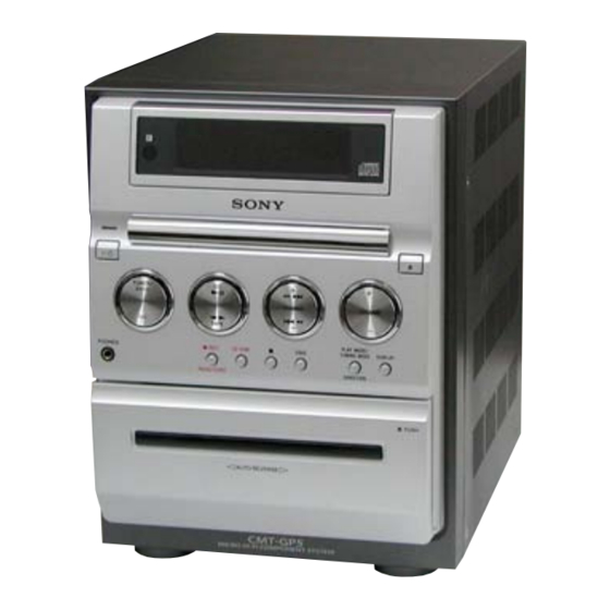
SERVICE MANUAL
Ver 1.6 2006.02
HCD-GP5 is the Amplifier, CD player, Tape
Deck and Tuner section in CMT-GP5.
Amplifier section
AUDIO POWER SPECIFICATIONS:
(U.S.A. model only)
POWER OUTPUT AND TOTAL HARMONIC
DISTORTION:
With 6-ohm loads, both channels driven, from 120 -
10,000 Hz; rated 35 watts per channel minimum RMS
power, with no more than 10% total harmonic
distortion from 250 milliwatts to rated output.
North American model:
Continuous RMS power output (reference):
35 + 35 W
(6 ohms at 1 kHz, 10%
THD)
European model:
DIN power output (rated): 30 + 30 W
(6 ohms at 1 kHz, DIN)
Continuous RMS power output (reference):
30 + 30 W
(6 ohms at 1 kHz, 10%
THD)
Music power output (reference):
60 + 60 W
Other models:
The following measured at AC 230 V or AC 120 V, 50/
60 Hz
DIN power output (rated): 30 + 30 W
(6 ohms at 1 kHz, DIN)
Continuous RMS power output (reference):
30 + 30 W
(6 ohms at 1 kHz, 10%
THD)
Sony Corporation
9-877-380-07
2006B16-1
Personal Audio Division
© 2006.02
Published by Sony Techno Create Corporation
HCD-GP5
Model Name Using Similar Mechanism
CD Mechanism Type
CD
Section
Base Unit Name
Optical Pick-up Name
Model Name Using Similar Mechanism
TAPE
Section
Tape Transport Mechanism Type
SPECIFICATIONS
Inputs
MD IN (phono jacks):
Sensitivity 500 mV,
impedance 47 kilohms
Outputs
PHONES (stereo minijack):
Accepts headphones with
an impedance of 8 ohms or
more
SPEAKERS:
Accepts impedance of 6 to
16 ohms.
CD player section
System
Compact disc and digital
audio system
Laser
Semiconductor laser
(
λ
=780 nm)
Emission duration:
continuous
Frequency response
2 Hz – 20 kHz (±0.5 dB)
Tape deck section
Recording system
4-track 2-channel stereo
Frequency response
50 – 13,000 Hz (±3 dB),
using Sony TYPE I
cassettes
Tuner section
FM stereo, FM/AM superheterodyne tuner
FM tuner section
MICRO HI-FI COMPONENT SYSTEM
US Model
Canadian Model
AEP Model
UK Model
E Model
Australian Model
NEW
CDM55A-K6BD44B
BU-K1BD44B
KSM-213D
NEW
CMAL1Z240A
Tuning range
87.5 – 108.0 MHz (50-kHz
step)
Antenna
FM lead antenna
Antenna terminals
75 ohms balanced
Intermediate frequency
10.7 MHz
AM tuner section
Tuning range
Pan-American model:
530 – 1,710 kHz
(with the tuning interval
set at 10 kHz)
531 – 1,710 kHz
(with the tuning interval
set at 9 kHz)
European model:
531 – 1,602 kHz
(with the tuning interval
set at 9 kHz)
Other models:
530 – 1,710 kHz
(with the tuning interval
set at 10 kHz)
531 – 1,602 kHz
(with the tuning interval
set at 9 kHz)
Antenna
AM loop antenna, external
antenna terminal
Intermediate frequency
450 kHz
— Continued on next page —
Advertisement
Table of Contents

Related Manuals for Sony HCD-GP5


Summary of Contents for Sony HCD-GP5
-
Page 1: Specifications
US Model Canadian Model Ver 1.6 2006.02 AEP Model UK Model E Model Australian Model HCD-GP5 is the Amplifier, CD player, Tape Deck and Tuner section in CMT-GP5. Model Name Using Similar Mechanism CD Mechanism Type CDM55A-K6BD44B Section Base Unit Name... -
Page 2: Table Of Contents
LES COMPOSANTS IDENTIFÉS PAR UNE MARQUE 0 SUR LES DIAGRAMMES SCHÉMATIQUES ET LA LISTE DES PIÈCES SONT CRITIQUES POUR LA SÉCURITÉ DE FONCTIONNEMENT. NE REMPLACER CES COMPOSANTS QUE PAR DES PIÈSES SONY DONT LES NUMÉROS SONT DONNÉS DANS CE MANUEL OU DANS LES SUPPÉMENTS PUBLIÉS PAR SONY. -
Page 3: Servicing Notes
HCD-GP5 SECTION 1 SERVICING NOTES Notes on chip component replacement CAUTION • Never reuse a disconnected chip component. Use of controls or adjustments or performance of procedures • Notice that the minus side of a tantalum capacitor may be dam- other than those specified herein may result in hazardous aged by heat. - Page 4 HCD-GP5 Service Position of the CD Mechanism Deck MAIN Board CD Mechanism Deck (CDM55A-K6BD44B) Service Position of the Tape Cassette Mechanism Deck MAIN Board Tape Cassette Mechanism Deck (CMAL1Z240A)
-
Page 5: General
HCD-GP5 SECTION 2 GENERAL This section is extracted from instruction manual. List of button locations and reference pages How to use this page Illustration number Use this page to find the location of buttons and other DISPLAY 8 (9, 10, 16) parts of the system that are mentioned in the text. -
Page 6: Setting The Clock
HCD-GP5 Remote control ALPHABETICAL ORDER BUTTON DESCRIPTIONS ?/1 (power) 1 (5, 9, 14, 15) A – M P – Z m/M (fast forward/rewind) BASS +/– 0 (13) PLAY MODE/DIRECTION qd 6 (6, 11) CLEAR 8 (8, 9) (6, 7, 11, 12, 15) ./>... -
Page 7: Disassembly
HCD-GP5 Ver 1.2 2003.11 SECTION 3 DISASSEMBLY • This set can be disassembled in the order shown below. TOP CABINET, REAR PANEL FRONT PANEL ASSY CD MECHANISM DECK CONTROL BOARD, (CDM55A-K6BD44B) SINGLE CASSETTE MECHANISM MAIN BOARD, LOADING BOARD CD BOARD... -
Page 8: Front Panel Assy
HCD-GP5 3-2. Front Panel Assy 4 four s crews (+BVTP 3 × 10) 5 w ire (flat type) 13p (CN303) 1 four claws 7 connector 5p (CN1) 6 w ire (flat type) 26p (CN302) q; front panel assy 2 CD lid... -
Page 9: Cd Mechanism Deck (Cdm55A-K6Bd44B)
HCD-GP5 3-4. CD Mechanism Deck (CDM55A-K6BD44B) 4 s crew (+BVTP 3 × 10) 1 CD plate 7 CD mechanism deck CN101 (CDM55A-K6BD44B) 3 w ire (flat type) 21p (CN101,305) 6 CD holder CN305 2 s crew (+BVTP 3 × 10) -
Page 10: Main Board, Transformer Board
HCD-GP5 3-5. MAIN Board, TRANSFORMER Board q; four s crews (+BVTP 3 × 10) 6 two s crews 1 connector 9p (CN801) (+BVTP 3 × 10) qs TRANSFORMER 8 sub heat sink board qa power transformer 7 two s crews (+BVTP 3 ×... -
Page 11: Cd Board
HCD-GP5 3-7. CD Board 1 screw(+P 2.6 × 5) wire (flat type) 21p (CN101) CD board Remove soldering from the four points. wire (flat type) 16p 3-8. Tray (CDM55D) 1 While pressing the two protrusions A and B to unlock the two claws as shown, pull the tray in the direction of the arrow C . -
Page 12: Optical Pick-Up (Ksm-213D), Holder (C213)
HCD-GP5 Ver 1.2 2003.11 3-9. Optical Pick-up (KSM-213D), Holder (C213) 2 two compression spring (T213) 3 insulator 5 screw (+PTTP M2.6) 1 two floating screws (+PTPWH M2.6) 6 stopper (BU) 7 compression spring 4 insulator (T213) 8 insulator 9 screw (+PTTP M2.6) q;... -
Page 13: Mechanical Adjustments
HCD-GP5 SECTION 4 MECHANICAL ADJUSTMENTS Precaution Clean the following parts with a denatured alcohol-moistened swab: record/playback heads pinch rollers erase head rubber belts capstan idlers Demagnetize the record/playback head with a head demag- netizer. Do not use a magnetized screwdriver for the adjustments. -
Page 14: Electrical Adjustments
HCD-GP5 SECTION 5 ELECTRICAL ADJUSTMENTS Mode: Playback DECK SECTION 0 dB=0.775V test tape Demagnetize the record/playback head with a head demagnetizer. MAIN board P-4-A100 J203 (10kHz, –10dB) Do not use a magnetized screwdriver for the adjustments. speaker terminal oscilloscope After the adjustments, apply suitable locking compound to the parts adjusted. - Page 15 HCD-GP5 RFDC signal waveform CD SECTION VOLT/DIV: 200 mV TIME/DIV: 500 ns Note: 1. CD Block is basically designed to operate without adjustment. There- fore, check each item in order given. 2. Use YEDS-18 disc (3-702-101-01) unless otherwise indicated. level: 0.7 ± 0.2 Vp-p 3.
- Page 16 HCD-GP5 E-F Balance Check Checking Location: Connection: – CD BOARD (Conductor Side) – oscilloscope CD board TP (TE) TP (DVC) – Procedure: Connect an oscilloscpe to test point TP (TE) and TP (DVC) on TP (VC) the CD board. AC is put in pushing CD button.
-
Page 17: Diagrams
HCD-GP5 Ver 1.3 2004.01 SECTION 6 DIAGRAMS • Circuit Boards Location CD board LOADING board TRANSFORMER board CONTROL board MAIN board HEADPHONE board THIS NOTE IS COMMON FOR PRINTED WIRING BOARDS AND SCHEMATIC DIAGRAMS. (In addition to this, the necessary note is printed in each block.) For schematic diagrams. - Page 18 HCD-GP5 • Waveforms – CD Board – – CONTROL Board – – MAIN Board – IC103 qg (RFAC) IC601 qd (O-XT2) Q301 collector (Rec mode) (CD Play Mode) 10.6Vp-p 1.1Vp-p 5.4Vp-p 10.9 µ s 30.5 µ s 5V/DIV, 5 µ s /DIV 200mV/DIV, 1 µ...
-
Page 19: Block Diagram
HCD-GP5 Ver 1.2 2003.11 6-1. Block Diagram POWER AMP PB/REC EQ AMP J201 IC301 IC201 AUX L OUT L L IN L OUT J202 µ CON TU L OUT R R-CH IC601 PHONES MUTE R-CH CD L R OUT Q504... -
Page 20: Printed Wiring Board - Cd Section
HCD-GP5 Ver 1.2 2003.11 6-2. Printed Wiring Board – CD Section – • See page 17 for Circuit Boards Location. • Semiconductor Location Ref. No. Location D101 IC101 IC102 IC103 Q101 Q102 TP (VC) IC102 IC103 TP (RFAC) TP (DVC) -
Page 21: Schematic Diagram - Cd Section
HCD-GP5 Ver 1.2 2003.11 6-3. Schematic Diagram – CD Section – • See page 18 for Waveforms. • See page 31, 32 for IC Block Diagrams. K S M - 2 1 3 D J R 1 0 1 4 7 0 p... -
Page 22: Printed Wiring Board - Control Section
HCD-GP5 Ver. 1.6 6-4. Printed Wiring Board – Control Section – • See page 17 for Circuit Boards Location. CONTROL BOARD • Semiconductor Location Ref. No. Location D601 D602 FLUORESCENT INDICATOR TUBE D603 D604 IC601 D605 US,CND,AEP,UK,KR D606 D607 E51,HK,SP,... -
Page 23: Schematic Diagram - Control Section
HCD-GP5 Ver. 1.6 6-5. Schematic Diagram – Control Section – • See page 18 for Waveforms. • See page 33 for IC Block Diagram. • See page 35 for IC Pin Function Description. IC603 CONTROL BOARD FLUORESCENT INDICATOR TUBE RPM7140-V4... -
Page 24: Printed Wiring Boards - Main Section
HCD-GP5 Ver 1.3 2004.01 6-6. Printed Wiring Boards – Main Section – MAIN BOARD • Semiconductor Location Ref. No. Location Ref. No. Location D301 Q302 Q303 D302 D303 Q304 D304 Q305 CONTROL TUNER CD BOARD D402 Q306 BOARD UNIT CN101... -
Page 25: Schematic Diagram - Main Section (1/4)
HCD-GP5 Ver. 1.6 6-7. Schematic Diagram – Main Section (1/4) – • See page 33 for IC Block Diagram. TUNER UNIT MAIN BOARD (1/4) CN302 AEP,UK,KR CN304 Q314 - Q316 Q316 10.2 (2.5) 2SA1980G (10.3) (1.0) CONTROL BOARD CN601 AEP, UK, KR... -
Page 26: Schematic Diagram - Main Section (2/4)
HCD-GP5 Ver. 1.6 6-8. Schematic Diagram – Main Section (2/4) – • See page 34 for IC Block Diagram. HEADPHONE BOARD MAIN BOARD (2/4) PHONES FB203 0.45uH *1 IC201 IC201 AEP,UK,KR MODELS : STK403-030 OTHER MODELS : STK403-040 POWER AMP... -
Page 27: Schematic Diagram - Main Section (3/4)
HCD-GP5 Ver. 1.6 6-9. Schematic Diagram – Main Section (3/4) – • See page 18 for Waveform. MAIN BOARD (1/4) (Page 25) MAIN BOARD (3/4) Q305 - Q311 REC/PLAY Q305 SWITCH 2SK2158-T2B (-0.4) (-0.4) Q308 2SK2158-T2B Q306 R331 DTA124EUA-T106 D301... -
Page 28: Schematic Diagram - Main Section (4/4)
HCD-GP5 Ver. 1.6 6-10. Schematic Diagram – Main Section (4/4) – MAIN BOARD (2/4) (Page 26) MAIN BOARD (4/4) MTZJ-T-77-33D 1N4003LES 1N4003LES -31.7 1N4003LES 2SA1979 -31.2 -34.5 Q413 0.047 1N4003LES 0.047 -VFL VOLTAGE REGULATOR PN401 TRANSFORMER MAIN BOARD BOARD 10.3 17.5... -
Page 29: Printed Wiring Board - Power Section
HCD-GP5 Ver. 1.6 6-11. Printed Wiring Board – Power Section – • See page 17 for Circuit Boards Location. E51,TW TRANSFORMER BOARD SW801 MAIN BOARD VOLTAGE PN401 SELECTOR (Page 24) POWER TRANSFORMER 220-240V 230V PT802 POWER TRANSFORMER (SUB) EXCEPT E51,TW... -
Page 30: Schematic Diagram - Power Section
HCD-GP5 Ver. 1.6 6-12. Schematic Diagram – Power Section – E51, TW TRANSFORMER BOARD PT801 POWER TRANSFORMER SW801 220-240V VOLTAGE SELECTOR MAIN 120V BOARD (4/4) PN401 not replaceable (Page 28) bult in transformer RY801 POWER RELAY CN801 D802 1SS133T-72 L801... -
Page 31: Ic Block Diagrams
HCD-GP5 • IC Block Diagrams – CD Board – IC101 CXD3017Q ERROR DIGITAL CORRECTOR DIGITAL ASYMMETRY CORRECTOR OPERATIONAL LRCK AMPLIFIER ANALOG SWITCH PCMD INTERFACE DEMODULATOR CONVERTER EMPH XVDD XTAI TIMING LOGIC CLOCK XTAO XTSL GENERATOR XVSS TES1 AVDD1 TEST AOUT1... - Page 32 HCD-GP5 IC103 CXA2581N-T4 RW/ROM DC OFST RFDCI – – RFDCO – RW/ROM VOFST APC AMP EQ ON/OFF RFAC EQ IN RW/ROM RFAC AC SUM SUMMING VOFST – – RW/ROM TE BAL RW/ROM – APC-OFF RW/ROM (Hi-Z) RW/ROM RW/ROM (H/L) DVCC VOFST –...
- Page 33 HCD-GP5 – CONTROL Board – IC604 BA6956AN CONTROL LOGIC – MAIN Board – IC301 BD3881FV...
- Page 34 HCD-GP5 IC201 STK403-040 PRE DRIVER PRE DRIVER IC CH1 IC CH2 BIAS CIRCUIT...
-
Page 35: Ic Pin Function Description
HCD-GP5 6-13. IC Pin Function Description IC601 LC876764A-51E5 System Control (CONTROL Board) Pin No. Pin Name Description C-PWM1 PWM1 signal output to the CD unit C-PWM2 PWM2 signal output to the CD unit C-SCOR SCOR (SUBQ request) signal output to the CD unit... - Page 36 HCD-GP5 Pin No. Pin Name Description R-CE Tuner chip enable signal output to the tuner C-XRST Reset signal output to the CD unit C-XLT Latch signal output to the CD unit C-DATA Data output to the CD unit C-SQCK SUBQ clock output to the CD unit VSS2 —...
-
Page 37: Exploded Views
HCD-GP5 Ver 1.5 SECTION 7 EXPLODED VIEWS NOTE: • -XX, -X mean standardized parts, so they may • Abbreviation The components identified by mark 0 or have some differences from the original one. : Australian model dotted line with mark 0 are critical for safety. -
Page 38: Front Panel Section
HCD-GP5 Ver 1.5 7-2. Front Panel Section supplied supplied supplied supplied supplied supplied Ref. No. Part No. Description Remark Ref. No. Part No. Description Remark 4-247-757-01 SPR-T,CASS 4-247-369-01 BUTTON,OPEN/CLOSE X-4955-860-1 LID TC ASSY 4-247-368-01 BUTTON,FUNCTION X-4955-859-1 HOLDER CASSETTE ASSY 4-231-841-01 SPRING (HEART CAM-B) -
Page 39: Chassis Section
HCD-GP5 Ver. 1.6 7-3. Chassis Section supplied not supplied PT801 supplied not supplied not supplied Ref. No. Part No. Description Remarks Ref. No. Part No. Description Remarks 0 PT801 4-247-752-01 RUBBER, FOOT 1-443-033-11 TRANSFORMER, POWER (AEP,UK) 1-689-574-11 TRANSFORMER BOARD (EXCEPT E51,TW) -
Page 40: Cd Mechanism Deck Setion
HCD-GP5 Ver 1.2 2003.11 7-4. CD Mechanism Deck Setion not supplied not supplied M901 optical pick-up (KSM-213D) Ref. No. Part No. Description Remarks Ref. No. Part No. Description Remarks A-4735-082-A MAGNET 1-674-336-12 LOADING BOARD 4-231-777-02 SHEET (KH2) 4-925-315-31 DAMPER 4-224-894-22 TRAY (CDM55D) -
Page 41: Ksm-213D
HCD-GP5 Ver 1.2 2003.11 7-5. KSM-213D Ref. No. Part No. Description Remarks 0 601 A-4735-357-A OPTICAL PICK-UP ASSY (KSM213DHAP/ZRP1) The components identified by Les composants identifiés par mark 0 or dotted line with mark une marque 0 sont critiques 0 are critical for safety. -
Page 42: Electrical Parts List
HCD-GP5 Ver. 1.6 SECTION 8 ELECTRICAL PARTS LIST NOTE: • Due to standardization, replacements in the parts • CAPACITORS: HK : Hong Kong model uF: µF list may be different from the parts specified in KR : Korean model the diagrams or the components used on the set. - Page 43 HCD-GP5 Ver. 1.6 CONTROL Ref. No. Part No. Description Remarks Ref. No. Part No. Description Remarks R117 1-216-821-11 METAL CHIP 1/10W C609 1-163-059-91 CERAMIC CHIP 0.01uF R118 1-216-809-11 METAL CHIP 1/10W C610 1-115-339-11 CERAMIC CHIP 0.1uF R119 1-216-826-11 METAL CHIP 2.7K...
- Page 44 HCD-GP5 Ver. 1.6 CONTROL Ref. No. Part No. Description Remarks Ref. No. Part No. Description Remarks D607 8-719-991-33 DIODE 1SS133T-77 R615 1-247-831-91 CARBON 1/4W D608 8-719-989-91 DIODE 1N4148A-T265 R616 1-247-831-91 CARBON 1/4W D609 8-719-989-91 DIODE 1N4148A-T265 R617 1-247-831-91 CARBON 1/4W...
- Page 45 HCD-GP5 Ver. 1.6 CONTROL HEADPHONE LOADING Ref. No. Part No. Description Remarks Ref. No. Part No. Description Remarks R675 1-216-837-11 METAL CHIP 1/10W R726 1-216-829-11 METAL CHIP 4.7K 1/10W R676 1-216-837-11 METAL CHIP 1/10W R727 1-216-845-11 METAL CHIP 100K 1/10W...
- Page 46 HCD-GP5 Ver. 1.6 MAIN Ref. No. Part No. Description Remarks Ref. No. Part No. Description Remarks A-4747-957-A MAIN BOARD, COMPLETE (AEP, UK, KR) C355 1-124-464-11 ELECT 0.22uF A-4747-962-A MAIN BOARD, COMPLETE (US, CND) C356 1-124-464-11 ELECT 0.22uF A-4748-777-A MAIN BOARD, COMPLETE...
- Page 47 HCD-GP5 Ver. 1.6 MAIN Ref. No. Part No. Description Remarks Ref. No. Part No. Description Remarks C504 1-162-970-11 CERAMIC CHIP 0.01uF D429 8-719-991-33 DIODE 1SS133T-77 C505 1-113-342-11 CERAMIC 0.1uF C506 1-163-021-91 CERAMIC CHIP 0.01uF D430 8-719-048-55 DIODE MTZJ-T-77-10C D431 6-500-335-01 DIODE MC2838-T112-1...
- Page 48 HCD-GP5 Ver. 1.6 MAIN Ref. No. Part No. Description Remarks Ref. No. Part No. Description Remarks Q314 8-729-120-28 TRANSISTOR 2SC1623-L5L6 R314 1-216-813-11 METAL CHIP 1/10W Q315 8-729-120-28 TRANSISTOR 2SC1623-L5L6 (AEP, UK, KR) R315 1-216-828-11 METAL CHIP 3.9K 1/10W Q316 6-550-296-01 TRANSISTOR...
- Page 49 HCD-GP5 Ver. 1.6 MAIN TRANSFORMER Ref. No. Part No. Description Remarks Ref. No. Part No. Description Remarks R374 1-216-826-11 METAL CHIP 2.7K 1/10W R457 1-216-841-11 METAL CHIP 1/10W R458 1-216-841-11 METAL CHIP 1/10W R377 1-249-434-11 CARBON 1/4W R459 1-216-829-11 METAL CHIP 4.7K...
- Page 50 HCD-GP5 Ver. 1.6 TRANSFORMER Ref. No. Part No. Description Remarks CN802 1-564-321-00 PIN, CONNECTOR (3.96mm PITCH) 2P < DIODE > D801 8-719-991-33 DIODE 1SS133T-77 D802 8-719-991-33 DIODE 1SS133T-77 D803 8-719-991-33 DIODE 1SS133T-77 D804 8-719-991-33 DIODE 1SS133T-77 < COIL > 0 L801 1-402-663-11 TRANSFORMER, LINE FILTER (LFT) <...
- Page 51 HCD-GP5 MEMO...
- Page 52 HCD-GP5 REVISION HISTORY Clicking the version allows you to jump to the revised page. Also, clicking the version at the upper right on the revised page allows you to jump to the next revised page. Ver. Date Description of Revision 2003.06...
Need help?
Do you have a question about the HCD-GP5 and is the answer not in the manual?
Questions and answers