Table of Contents
Advertisement
SERVICE MANUAL
HCD-SD1 is the amplifier, CD and
tuner section in CMT-SD1.
MICROFILM
HCD-SD1
Model Name Using Similar Mechanism
CD
Mechanism Type
SECTION
Base Unit Type
Optical Pick-up Type
SPECIFICATIONS
COMPACT DISC RECEIVER
– 1 –
AEP Model
UK Model
E Model
HCD-MD313
CDM13B-5BD19
BU-5BD19
KSS-213B/K-N
— Continued on next page —
Advertisement
Table of Contents

Related Manuals for Sony HCD-SD1


Summary of Contents for Sony HCD-SD1
- Page 1 HCD-SD1 SERVICE MANUAL AEP Model UK Model E Model HCD-SD1 is the amplifier, CD and tuner section in CMT-SD1. Model Name Using Similar Mechanism HCD-MD313 Mechanism Type CDM13B-5BD19 SECTION Base Unit Type BU-5BD19 Optical Pick-up Type KSS-213B/K-N SPECIFICATIONS — Continued on next page —...
- Page 2 THE PARTS LIST ARE CRITICAL TO SAFE OPERATION. SP, HK model 4-212-712-0π REPLACE THESE COMPONENTS WITH SONY PARTS WHOSE PART NUMBERS APPEAR AS SHOWN IN THIS • Abbreviation MANUAL OR IN SUPPLEMENTS PUBLISHED BY SONY. : Hong Kong model : Singapore model – 2 –...
-
Page 3: Table Of Contents
TABLE OF CONTENTS NOTES ON HANDLING THE OPTICAL PICK-UP BLOCK OR BASE UNIT 1. SERVICING NOTE ............4 The laser diode in the optical pick-up block may suffer electrostatic 2. GENERAL ................7 break-down because of the potential difference generated by the charged electrostatic load, etc. -
Page 4: Servicing Note
SECTION 1 SERVICING NOTE OPENING THE DISC TRAY WHEN POWER IS OFF 2 Open the glass door, and pull out the loading panel. 1 Using a thin screwdriver, rotate the internal cam in the arrow direction completely. ATTACHING THE GLASS ASSEMBLY •... - Page 5 POSITIONS FOR SERVICING THE CONNECTOR BOARD, SUB-TRANS BOARD, CHEMI-CON BOARD, AND AMP BOARD 1 Remove the four screws securing the upper cover, and remove the upper cover. 2 Remove the loading panel. (Refer to SECTION 3 DISASSEM- BLY.) 3 Remove the four screws A securing the MAIN board, five screws B securing the rear panel, two flat cables (CN701, CN702), and open the MAIN board as shown in the figure.
- Page 6 POSITION FOR SERVICING THE CD MECHANISM DECK 1 Remove the four screws securing the upper cover, and remove the upper cover. 2 Remove the loading panel. (Refer to SECTION 3 DISASSEM- BLY.) 3 Remove the four screws A securing the MAIN board, five screws B of the rear panel, and flat cables (CN701, CN702), and re- move the MAIN board.
-
Page 7: General
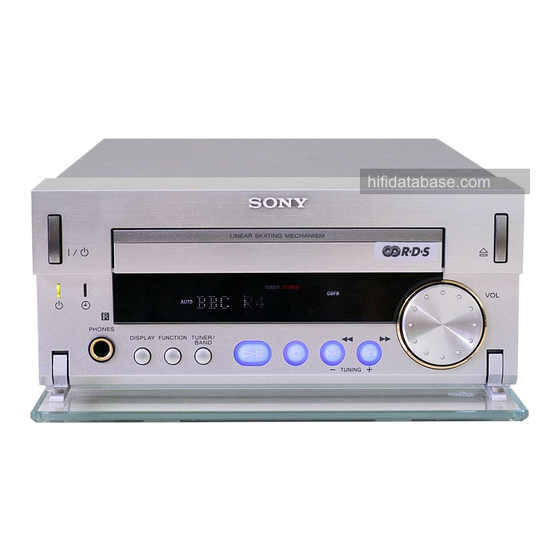
SECTION 2 GENERAL Front Panel Location of Parts and Controls 6 ≠/0/TUNING – button 11 DISPLAY button 1 1/u (Power) button 7 π button 12 PHONES jack 2 CD disc tray 13 t indicator 8 fl button 3 § button 14 u indicator 9 TUNER/BAND button 4 VOLUME dial... -
Page 8: Disassembly
SECTION 3 DISASSEMBLY Note: Follow the disassembly procedure in the numerical order given. 3-1. LOADING PANEL 1 Turn ON the power, and press the EJECT button to open the tray. 2 Remove the loading panel in the arrow direction. 3 Press the EJECT button to close the tray. •... -
Page 9: Front Panel
3-3. FRONT PANEL 4 Flat type wire (11core) (CN702) 6 Front panel 2 Three claws 5 Flat type wire (13core) (CN701) 1 Three screws (BVTP3x8) 3-4. MAIN BOARD AND TUNER UNIT 1 Four screws (BVTP3x8) 7 MAIN board and Tuner unit 6 Flat type wire (19core) (CN705) 8 Connector (CN706) -
Page 10: Cd Mechanism Deck
3-5. CD MECHANISM DECK 6 Three screws (BVTP3x8) 7 Dust cover 9 CD mechanism deck 8 Two screws 3 Connector (BVTP3x8) (CN942) 5 REG board 1 Two screws (BVTP3x8) 2 Connector (CN945) 4 Connector (CN994) 3-6. BACK PANEL 2 Four screws 7 Back panel (BVTT3X8) 5 Connector... -
Page 11: Disc Table
3-7. DISC TABLE 3 Holder (MG) assembly 1 Screw (BV3x8) 2 Screw (BV3x8) 4 Pull out the disc table. 3-8. OPTICAL PICK-UP 4 Remove the optical pickup in the arrow direction C . 3 Flat type wire (16 core) (CNU101) 1 Move the claw in the arrow A direction. -
Page 12: Service Mode
SECTION 4 SERVICE MODE Key Check Mode for Complete Lighting of LED/Fluorescent Display Tube • Perform this mode to analyze and check malfunctions such as display defects and when buttons do not work. Procedure: 1. Press the 1/u button to turn on the power. 2. -
Page 13: Test Mode
SECTION 5 TEST MODE AGING MODE This unit is equipped with an aging mode. Use this mode for analyzing defects and for checks after completing repairs. After repairs, perform aging 100 times and check that the unit is normal. The aging mode is executed in the following sequence. The aging mode will continue as long as the unit is normal. -
Page 14: Electrical Adjustments
SECTION 6 ELECTRICAL ADJUSTMENTS S Curve Check CD SECTION oscilloscope Note: BD (CD) board 1. CD Block is basically designed to operate without adjustment. Therefore, check each item in order given. TP (FEO) 2. Use YEDS-18 disc (3-702-101-01) unless otherwise indicated. TP (VC) –... - Page 15 E-F Balance (1 Track Jump) Check Adjustment Location: (Without remote commander) [BD (CD) BOARD] — Component Side — oscilloscope BD (CD) board (Focus Bias Adjust) TP (TEO) RV101 TP (VC) – IC101 RV103 Procedure : 1. Connect oscilloscpe to test point TP (TEO) on BD board. 2.
-
Page 16: Diagrams
SECTION 7 DIAGRAMS 7-1. CIRCUIT BOARDS LOCATION TRANS board MAIN board PANEL-SW board SUB-TRANS board BD board LOADING board AMP board REG board CHEMI-CON board PANEL board HP board CONNECTOR board VOLUME board – 16 –... -
Page 17: Block Diagrams
HCD-SD1 7-2. BLOCK DIAGRAMS – BD SECTION – OPTICAL PICK-UP (KSS-213B) X101 22.5792 MHz TRACKING/FOCUS SERVO, RF AMP 5 • 6 DETECTOR DIGITAL FILTER IC101 (1/2) D/A CONVERTER IC104 MAIN DATA LOUT 16 PCMD CD LOUT SECTION LRCK LRCK DIGITAL SIGNAL PROCESSOR... - Page 18 HCD-SD1 – MAIN SECTION – SOUND PROCESSOR TUNER IC101(1/2) ANTENNA UNIT SOUND PROCESSOR POWER AMP IC101(2/2) IC801 SPEAKER RELAY TUNER L-OUT RY501 TMB11 BS/CS R-OUT R-CH DBFB – BASS/ STEREO R-CH MUTE DEFB SW R-CH R-CH SPEAKER TREBLE – Q141...
- Page 19 THIS NOTE IS COMMON FOR PRINTED WIR- ING BOARDS AND SCHEMATIC DIAGRAMS. (In addition to this, the necessary note is printed in each block.) For schematic diagrams. Note: • All capacitors are in µF unless otherwise noted. pF: µµF 50 WV or less are not indicated except for electrolytics and tantalums.
-
Page 20: Main Section
WAVEFORMS – MAIN SECTION – – BD SECTION – 1.3 ± 0.3 Vp-p 4.3 Vp-p IC101 #¡ (RFO) (PLAY Mode) 5 MHz IC701 !¡ (XI) 500 mV/DIV, 500 ns/DIV Approx. 100 mVp-p 2.6 Vp-p 32 kHz IC101 $¢ (TEI) (PLAY Mode) 50 mV/DIV, 1 µs/DIV IC701 !¢... -
Page 21: Schematic Diagram - Bd Section
HCD-SD1 7-3. SCHEMATIC DIAGRAM – BD SECTION – • See page 22 for Waveforms. • See page 51 for IC Block Diagrams. (Page 29) Note on Schematic Diagram: • Voltages and waveforms are dc with respect to ground under no-signal (detuned) conditions. -
Page 22: Printed Wiring Board - Bd Section
HCD-SD1 7-4. PRINTED WIRING BOARD – BD SECTION – • See page 16 for Circuit Boards Location. (Page 32) OPTICAL PICK-UP BLOCK KSS-213BA/S-N • Semiconductor • Semiconductor Location Location Ref. No. Location Ref. No. Location IC103 IC101 IC102 Q101 IC104... -
Page 23: Schematic Diagram - Main (1/2) Section
HCD-SD1 7-5. SCHEMATIC DIAGRAM – MAIN (1/2) SECTION – • See page 22 for Waveforms. • See page 31 for Printed Wiring Board. (Page 39) (Page (Page – 27 – – 28 –... -
Page 24: Schematic Diagram - Main (2/2) Section
HCD-SD1 7-6. SCHEMATIC DIAGRAM – MAIN (2/2) SECTION – • See page 22 for Waveforms. • See page 31 for Printed Wiring Board. • See page 53 for IC Block Diagrams. • See page 54 for IC Pin Functions. (Page 24) -
Page 25: Printed Wiring Board - Main Section
HCD-SD1 7-7. PRINTED WIRING BOARD – MAIN SECTION – • See page 16 for Circuit Boards Location. (Page 45) (Page 41) (Page 46) (Page 26) • Semiconductor Location Ref. No. Location D351 D751 D752 AEP, UK D753 (Page 37) D755... -
Page 26: Schematic Diagram - Sub Trans Section
HCD-SD1 7-8. SCHEMATIC DIAGRAM – SUB SECTION – 7-9. PRINTED WIRING BOARD – SUB SECTION – • See page 16 for Circuit Boards Location. (Page 49) (Page 47) DTC114ESA 11EQS04 11EQS04 (Page 43) 11EQS04 DTA114ESA-TP 11EQS04 11ES2-NTA2B 11ES2- DTA114ESA-TP NTA2B... -
Page 27: Schematic Diagram - Panel Section
HCD-SD1 7-10. SCHEMATIC DIAGRAM – PANEL SECTION – (Page 30) (Page 30) – 35 – – 36 –... -
Page 28: Printed Wiring Board - Panel Section
HCD-SD1 7-11. PRINTED WIRING BOARD – PANEL SECTION – • See page 16 for Circuit Boards Location. (Page 32) (Page 32) • Semiconductor Location Ref. No. Location D601 D602 D603 D604 D605 D606 AEP, UK IC601 IC602 Q601 – 37 –... -
Page 29: Schematic Diagram - Amp Section
HCD-SD1 7-12. SCHEMATIC DIAGRAM – AMP SECTION – (Page 47, 48) (Page 43) (Page 28) – 39 – – 40 –... -
Page 30: Printed Wiring Board - Amp Section
HCD-SD1 7-13. PRINTED WIRING BOARD – AMP SECTION – • See page 16 for Circuit Boards Location. • Semiconductor Location Ref. No. Location D553 D554 D971 D972 Q505 Q551 Q552 Q553 (Page 50) (Page 31) (Page 45) – 41 –... -
Page 31: Schematic Diagram - Connector Section
HCD-SD1 7-14. SCHEMATIC DIAGRAM – CONNECTOR SECTION – (Page 30) (Page 40) (Page 29) (Page 33) – 43 – – 44 –... -
Page 32: Printed Wiring Board - Connector Section
HCD-SD1 7-15. PRINTED WIRING BOARD – CONNECTOR SECTION – • See page 16 for Circuit Boards Location. (Page 31, 32) • Semiconductor Location Ref. No. Location D501 D556 D557 D881 IC311 Q501 Q502 Q503 Q504 (Page 34) DIGITAL OPTICAL CD AUX... -
Page 33: Schematic Diagram - Reg Section
HCD-SD1 7-16. SCHEMATIC DIAGRAM – REG SECTION – (Page 40) (Page 29) (Page 29) (Page 33) – 47 – – 48 –... -
Page 34: Printed Wiring Board - Reg Section
HCD-SD1 7-17. PRINTED WIRING BOARD – REG SECTION – • See page 16 for Circuit Boards Location. OUTLET MDS-SD1 ONLY UNSWITCHED 200W MAX NOT REPLACEABLE: BUILT IN TRANSFORMER (Page 32) (Page 32) (Page 42) (Page 34) • Semiconductor Location Ref. No. -
Page 35: Ic Block Diagrams
HCD-SD1 7-18. IC BLOCK DIAGRAMS IC102 BA6397FP • BD section IC101 CXA1782BQ DRIVE DRIVE DRIVE BUFFER BUFFER BUFFER DRIVE BUFFER – REGULATOR LEVELS DRIVER MUTE 24 SENS – MIRR RF IV AMP1 DFCT 23 C. OUT DRIVE DRIVE DRIVE DRIVE... - Page 36 IC104 PCM1710U-R LRCIN ML/DSD INPUT MC/DM2 INTERFACE DIGITAL MODE FILTER CONTROL BCKIN MD/DM1 TIMING CLKO MUTE CONTROL MODE CKSL NOISE SHAPER DGND DGND 5-LEVEL DAC 5-LEVEL DAC RIGHT LEFT GND2R GND2L LOW-PASS FILTER LOW-PASS FILTER RIGHT LEFT EXT1R EXT1L 3-STAGE AMP 3-STAGE AMP EXT2R EXT2L...
-
Page 37: Ic Pin Functions
7-19. IC PIN FUNCTIONS • IC701 System Control (µPD780018AYGF-015-3BA) (MAIN Board) Function Pin No. Pin Name BD POWER CD power control pin, “H”:CD POWER ON PANEL SW Front cover open/close switch, “H”:Open glass door, “L”:Close glass door 3 to 7 –... - Page 38 Pin No. Pin Name Function LOAD IN Tray loading motor control signal, “L”:Loading LOAD OUT Tray loading motor control signal, “L”:When OPEN BD.RESET IC reset signal for CD control, “L”:RESET LIGHT BLUE LED control port of front panel, “L”:LED ON SDATA Serial data for SOUND PROCESSOR IC101 (M62428AFP) SCLOCK...
-
Page 39: Exploded Views
X-4950-580-1 GLASS ASSY (CD) 4-951-620-01 SCREW (2.6X8), +BVTP 4-212-584-01 BRACKET (SHAFT) 1-769-940-11 WIRE (FLAT TYPE) (11 CORE) 4-993-007-01 SCREW (M2.6X6), +P TAPPING 4-942-636-21 EMBLEM (NO.3.5), SONY 1-769-972-11 WIRE (FLAT TYPE) (13 CORE) 4-212-538-11 PANEL (AL-CD), FRONT * 17 1-671-609-11 HP BOARD... -
Page 40: Chassis Section
8-2. CHASSIS SECTION not supplied not supplied T991 not supplied (UK,HK) CN904 supplied M551 CDM13B-5BD19 supplied not supplied not supplied The components identified by mark ! or dotted line with mark ! are critical for safety. Replace only with part number specified. Ref. -
Page 41: Mechanism Deck Section (Cdm13B-5Bd19)
8-3. MECHANISM DECK SECTION (CDM13B-5BD19) not supplied BU-5BD19 M904 not supplied Ref. No. Part No. Description Remark Ref. No. Part No. Description Remark * 201 1-634-461-11 LOADING BOARD 4-944-012-01 TABLE, DISC 4-927-654-01 WASHER (LIMITER) A-4604-752-A HOLDER (MG) ASSY 3-659-338-00 SPRING, COMPRESSION * 213 4-917-583-21 BRACKET, YOKE 4-929-764-01 SHAFT (TABLE GUIDE) -
Page 42: Base Unit Section (Bu-5Bd19)
8-4. BASE UNIT SECTION (BU-5BD19) M101 M102 The components identified by mark ! or dotted line with mark ! are critical for safety. Replace only with part number specified. Ref. No. Part No. Description Remark Ref. No. Part No. Description Remark 4-951-620-01 SCREW (2.6X8), +BVTP 4-917-567-01 GEAR (M) -
Page 43: Electrical Parts List
SECTION 9 ELECTRICAL PARTS LIST Note: • Due to standardization, replacements in the parts list • SEMICONDUCTORS The components identified by In each case, u: µ , for example: may be different from the parts specified in the mark ! or dotted line with mark uA...: µ... - Page 44 CHEMI-CON Ref. No. Part No. Description Remark Ref. No. Part No. Description Remark < CONNECTOR > R145 1-216-097-91 RES,CHIP 100K 1/10W R146 1-216-097-91 RES,CHIP 100K 1/10W CNU101 1-770-014-11 CONNECTOR, FFC/FPC 16P R147 1-216-049-91 RES,CHIP 1/10W CNU102 1-770-013-11 CONNECTOR, FFC/FPC 19P R148 1-216-049-91 RES,CHIP 1/10W...
- Page 45 CHEMI-CON CONNECTOR LOADING Ref. No. Part No. Description Remark Ref. No. Part No. Description Remark < RESISTOR > L861 1-420-872-00 COIL, AIR-CORE R505 1-216-097-91 RES,CHIP 100K 1/10W < TRANSISTOR > R506 1-216-085-00 METAL CHIP 1/10W R551 1-216-049-91 RES,CHIP 1/10W Q501 8-729-029-66 TRANSISTOR DTC114ESA R552 1-216-097-91 RES,CHIP...
- Page 46 MAIN Ref. No. Part No. Description Remark Ref. No. Part No. Description Remark A-4419-059-A MAIN BOARD, COMPLETE (AEP,UK) C234 1-136-165-00 FILM 0.1uF C235 1-136-165-00 FILM 0.1uF ******************** C237 1-126-961-11 ELECT 2.2uF A-4419-070-A MAIN BOARD, COMPLETE (SP,HK) C241 1-126-043-11 ELECT 0.47uF C242 1-126-963-11 ELECT 4.7uF...
- Page 47 MAIN Ref. No. Part No. Description Remark Ref. No. Part No. Description Remark CN702 1-785-462-11 SOCKET, CONNECTOR (NON-ZIF)11P L405 1-410-482-31 INDUCTOR 100uH CN703 1-770-380-11 CONNECTOR, BOARD TO BOARD 8P CN704 1-770-380-11 CONNECTOR, BOARD TO BOARD 8P < TRANSISTOR > CN705 1-695-342-31 PIN, CONNECTOR (PC BOARD) 19P Q103 8-729-900-53 TRANSISTOR DTC114EK...
- Page 48 MAIN PANEL Ref. No. Part No. Description Remark Ref. No. Part No. Description Remark R191 1-249-413-11 CARBON 1/4W F R706 1-216-073-00 METAL CHIP 1/10W R192 1-249-413-11 CARBON 1/4W F R707 1-216-073-00 METAL CHIP 1/10W R193 1-249-413-11 CARBON 1/4W F R708 1-216-097-91 RES,CHIP 100K 1/10W...
- Page 49 PANEL PANEL-SW Ref. No. Part No. Description Remark Ref. No. Part No. Description Remark C604 1-163-141-00 CERAMIC CHIP 0.001uF S622 1-762-875-21 SWITCH, KEYBOARD (±/), TUNING +) C605 1-162-290-31 CERAMIC 470PF S623 1-762-875-21 SWITCH, KEYBOARD (≠/0, TUNING -) S624 1-762-875-21 SWITCH, KEYBOARD (π) C607 1-163-038-91 CERAMIC CHIP 0.1uF...
- Page 50 SUB-TRANS TRANS Ref. No. Part No. Description Remark Ref. No. Part No. Description Remark D945 8-719-986-04 DIODE HZS9A1LTA D962 8-719-024-99 DIODE 11ES2-NTA2B D946 8-719-986-04 DIODE HZS9A1LTA D963 8-719-024-99 DIODE 11ES2-NTA2B D952 8-719-986-26 DIODE HZS12A3LTA D964 8-719-024-99 DIODE 11ES2-NTA2B < GROUND TERMINAL > D965 8-719-986-67 DIODE HZS33-2LTA D966...
- Page 51 HCD-SD1 TRANS VOLUME Ref. No. Part No. Description Remark < THERMISTOR(POSITIVE) > THP944 1-801-726-11 THERMISTOR, POSITIVE THP945 1-801-726-11 THERMISTOR, POSITIVE ************************************************************** 1-671-610-11 VOLUME BOARD ************ < CAPACITOR > C691 1-162-306-11 CERAMIC 0.01uF C692 1-162-306-11 CERAMIC 0.01uF < CONNECTOR > * CLP691 1-690-880-31 LEAD (WITH CONNECTOR) <...
Need help?
Do you have a question about the HCD-SD1 and is the answer not in the manual?
Questions and answers