Table of Contents
Advertisement
HCD-GPX555/GPX888
SERVICE MANUAL
Ver. 1.1 2014.10
• HCD-GPX555 is the amplifi er, USB, CD player,
Bluetooth, NFC and tuner section in MHC-GPX555.
• HCD-GPX888 is the amplifi er, USB, CD player,
Bluetooth, NFC and tuner section in MHC-GPX888.
• "WALKMAN" and "WALKMAN" logo are registered trademarks of Sony Corporation.
• MPEG Layer-3 audio coding technology and patents licensed from Fraunhofer IIS and Thomson.
• Windows Media is either a registered trademark or trademark of Microsoft Corporation in the United States and/or
other countries.
• This product is protected by certain intellectual property rights of Microsoft Corporation. Use or distribution of
such technology outside of this product is prohibited without a license from Microsoft or an authorized Microsoft
subsidiary.
• The Bluetooth
®
word mark and logos are registered trademarks owned by Bluetooth SIG, Inc. and any use of such
marks by Sony Corporation is under license. Other trademarks and trade names are those of their respective owners.
• The N Mark is a trademark or registered trademark of NFC Forum, Inc. in the United States and in other countries.
• Android™ is a trademark of Google Inc.
• Google Play™ is a trademark of Google Inc.
• iPhone and iPod touch are trademarks of Apple Inc., registered in the U.S. and other countries. App Store is a service
mark of Apple Inc.
• "Made for iPod" and "Made for iPhone" mean that an electronic accessory has been designed to connect specifically
to iPod or iPhone, respectively, and has been certified by the developer to meet Apple performance standards. Apple is
not responsible for the operation of this device or its compliance with safety and regulatory standards. Please note that
the use of this accessory with iPod or iPhone may affect wireless performance.
• All other trademarks and registered trademarks are of their respective holders. In this manual, ™ and ® marks are not
specified.
AUDIO POWER SPECIFICATIONS
POWER OUTPUT AND TOTAL HARMONIC
DISTORTION:
(USA model only)
With 4 ohm loads, both channels driven, from
120 – 10,000 Hz; rated 180 watts per channel
minimum RMS power, with no more than
0.7% total harmonic distortion from 250
milliwatts to rated output.
Amplifi er section
The following are measured at
USA model:
AC 120 V, 60 Hz
Mexican model:
AC 120 V – 240 V, 60 Hz
Chilean and Bolivian models:
AC 220 V – 240 V, 50 Hz
Other models:
AC 120 V – 240 V, 50/60 Hz
MHC-GPX888
Front speaker
Power Output (rated):
350 W + 350 W (at 4 ohms, 1 kHz,
1% THD)
RMS output power (reference):
600 W + 600 W (per channel at
4 ohms, 1 kHz)
LBT-GPX555/MHC-GPX555
Front speaker
Power Output (rated):
350 W + 350 W (at 4 ohms, 1 kHz,
1% THD)
RMS output power (reference):
600 W + 600 W (per channel at 4 ohms,
1 kHz)
Subwoofer
RMS output power (reference):
600 W (4 ohms, 100 Hz)
9-890-651-02
Sony Corporation
2014J80-1
©
2014.10
Published by Sony EMCS (Malaysia) PG Tec
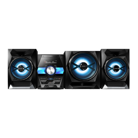
Photo: HCD-GPX888
SPECIFICATIONS
Inputs
AUDIO IN 1/PARTY CHAIN IN L/R
Voltage 2 V, impedance 47 kilohms
AUDIO IN 2 L/R
Voltage 2 V, impedance 47 kilohms
MIC (MHC-GPX888 only)
Sensitivity 1 mV, impedance
10 kilohms
(USB) A,
(USB) B, port
Type A
Outputs
AUDIO OUT/PARTY CHAIN OUT L/R
Voltage 2 V, impedance 1 kilohm
USB section
Supported bit rate
WMA:
48 kbps – 192 kbps, VBR, CBR
AAC:
48 kbps – 320 kbps, VBR, CBR
Sampling frequencies
WMA: 44.1 kHz
AAC: 44.1 kHz
Supported USB device
Mass Storage Class
Maximum current
500 mA
Disc/USB section
Supported bit rate
MPEG1 Layer-3:
32 kbps – 320 kbps, VBR
MPEG2 Layer-3:
8 kbps – 160 kbps, VBR
MPEG1 Layer-2:
32 kbps – 384 kbps, VBR
Sampling frequencies
MPEG1 Layer-3:
32 kHz/44.1 kHz/48 kHz
MPEG2 Layer-3:
16 kHz/22.05 kHz/24 kHz
MPEG1 Layer-2:
32 kHz/44.1 kHz/48 kHz
Model Name Using
Similar Mechanism
CD Section
CD Mechanism Type
Optical Pick-up Name
Disc player section
System
Compact disc and digital audio system
Laser Diode Properties
Emission Duration: Continuous
Laser Output*: Less than 44.6 W
* This output is the value measurement
at a distance of 200 mm from the
objective lens surface on the Optical
Pick-up Block with 7 mm aperture.
Frequency response
20 Hz – 20 kHz
Signal-to-noise ratio
More than 90 dB
Dynamic range
More than 88 dB
Tuner section
FM stereo, FM/AM superheterodyne tuner
Antenna:
FM lead antenna
AM loop antenna
FM tuner section
Tuning range
USA model:
87.5 MHz – 108.0 MHz
(100 kHz step)
Other models:
87.5 MHz – 108.0 MHz (50 kHz step)
AM tuner section
Tuning range
Pan American and Australian models:
531 kHz – 1,710 kHz (9 kHz step)
530 kHz – 1,710 kHz (10 kHz step)
Other models:
531 kHz – 1,602 kHz (9 kHz step)
530 kHz – 1,610 kHz (10 kHz step)
COMPACT DISC RECEIVER
US Model
HCD-GPX555
E Model
HCD-GPX555/GPX888
Australian Model
HCD-GPX555
HCD-GPX33
CDM90-DVBU204//M
CMS-S76RFS7G
Bluetooth section
Communication system
Bluetooth Standard version 3.1
Output
Bluetooth Standard Power Class 2
Maximum communication range
Line of sight approx. 10 m
1)
Frequency band
2.4 GHz band (2.4000 GHz – 2.4835 GHz)
Modulation method
FHSS (Freq Hopping Spread Spectrum)
Compatible Bluetooth profiles
2)
A2DP (Advanced Audio Distribution
Profile)
AVRCP 1.3 (Audio Video Remote
Control Profile)
SPP (Serial Port Profile)
Supported codecs
SBC (Sub Band Codec)
AAC (Advanced Audio Coding)
1)
The actual range will vary depending on
factors such as obstacles between devices,
magnetic fields around a microwave oven,
static electricity, reception sensitivity,
antenna's performance, operating system,
software application, etc.
2)
Bluetooth standard profiles indicate the
purpose
of
Bluetooth
communication
between devices.
– Continued on next page –
Advertisement
Table of Contents

Related Manuals for Sony HCD-GPX555


Summary of Contents for Sony HCD-GPX555
- Page 1 CMS-S76RFS7G marks by Sony Corporation is under license. Other trademarks and trade names are those of their respective owners. • The N Mark is a trademark or registered trademark of NFC Forum, Inc. in the United States and in other countries.
- Page 2 COMPONENTS IDENTIFIED BY MARK 0 OR DOTTED LINE WITH MARK 0 ON THE SCHEMATIC DIAGRAMS AND IN THE PARTS LIST ARE CRITICAL TO SAFE OPERATION. REPLACE THESE COMPONENTS WITH SONY PARTS WHOSE PART NUMBERS APPEAR AS SHOWN IN THIS MANUAL OR IN SUPPLEMENTS PUBLISHED BY SONY.
-
Page 3: Table Of Contents
HCD-GPX555/GPX888 TABLE OF CONTENTS SERVICING NOTES 6-19. Printed Wiring Board ..........- FL Board (Component side) - ........42 DISASSEMBLY 6-20. Printed Wiring Board - FL Board (Conductor side) -......... 43 2-1. Disassembly Flow ............6-21. Schematic Diagram - FL Board - ........44 2-2. -
Page 4: Servicing Notes
HCD-GPX555/GPX888 Ver. 1.1 SECTION 1 SERVICING NOTES MODEL IDENTIFICATION NOTES ON HANDLING THE OPTICAL PICK-UP – Back Panel – BLOCK OR BASE UNIT The laser diode in the optical pick-up block may suffer electro- static break-down because of the potential difference generated by the charged electrostatic load, etc. - Page 5 HCD-GPX555/GPX888 HOW TO OPEN THE TRAY WHEN POWER SWITCH TURN OFF Note 1: After the side panel (L, R) and top panel is removed, this work is done. Note 2: Please prepare the thin wire (clip etc. processed to the length of 8 cm or more).
- Page 6 – you may have to press N twice. Bluetooth device. – you may need to start playback of an audio source on the For example, select “SONY:MHC-GPX888” (or LBT- Bluetooth device. GPX555/MHC-GPX555). If passkey is required on the Bluetooth device, enter “0000”.
-
Page 7: Disassembly
HCD-GPX555/GPX888 SECTION 2 DISASSEMBLY • This set can be disassembled in the order shown below. 2-1. DISASSEMBLY FLOW 2-2. SIDE-L PANEL, SIDE-R PANEL, TOP PANEL (Page 8) 2-3. LOADING PANEL 2-4. FRONT PANEL SECTION 2-5. CD MECHANISM SECTION (Page 8) -
Page 8: Side-L Panel, Side-R Panel, Top Panel
HCD-GPX555/GPX888 Note: Follow the disassembly procedure in the numerical order given. 2-2. SIDE-L PANEL, SIDE-R PANEL, TOP PANEL 2 one screw qs four hooks (+BVTP 3 4 two claws 1 one screw (+BVTP 3 qd panel, top 2 one screw... -
Page 9: Front Panel Section
HCD-GPX555/GPX888 2-4. FRONT PANEL SECTION 2 two screws (+BVTP 3 6 CN451 (10P) (GPX888) 7 CN601 (4P) 8 front panel section DJ KEYS board 5 wire (flat type) (10 core) (CN102) (GPX555: US) 3 wire (flat type) (8 core) (CN105) -
Page 10: Back Panel Section
HCD-GPX555/GPX888 2-6. BACK PANEL SECTION 2 four screws (+BVTP 3 3 one screw (+BVTP 3 5 holder, wire 7 back panel section 6 sheet, service cover 4 one screw (+BVTP 3 1 wire (flat type) (9 core) (CN851) 2-7. MB BOARD, DAMP BOARD... -
Page 11: Switching Regulator (3H401W)
HCD-GPX555/GPX888 2-8. SWITCHING REGULATOR (3H401W) 6 two screws (+BVTP 3 7 sub, chassis 1 two screws (+BVTP 3 4 bracket, fan 6 two screws (+BVTP 3 3 two screws 5 DC fan (+BVTP 3 0 nine screws (+PWH 3 8 (SUMITITE)) -
Page 12: Service Optical Device, Wire (Flat Type)
HCD-GPX555/GPX888 2-9. SERVICE OPTICAL DEVICE, WIRE (FLAT TYPE) Note 1 : Before disconnecting the wire (fl at type) (24 core) of service optical device, solder the short-land. 1 six claws 2 chuck holder assy (T) qa insulator 8 four insulator screws... -
Page 13: Test Mode
HCD-GPX555/GPX888 SECTION 3 TEST MODE [PANEL TEST MODE] [COLD RESET] This mode is used to check the fl uorescent indicator tube, LEDs, The cold reset clears all data including preset data stored in the keys, [VOLUME / DJ CONTROL] jog, model, destination and data fl... - Page 14 HCD-GPX555/GPX888 [HISTORY MODE] This mode is used to check important data stored in the system when PROTECTOR happen. Procedure: 1. During demo mode, press [OPTIONS] button and [FLANGER] for 5 seconds to mode in to history mode. 2. Press the [M >...
- Page 15 HCD-GPX555/GPX888 [MODEL & DEST WRITE MODE] This mode is used to set software model & destination. This mode only available when no permanent model & destination is stored. Procedure: 1. Press [MOVIE/GAME] button & [LED PATTERN] button simultaneously and hold for 5 seconds.
-
Page 16: Electrical Check
HCD-GPX555/GPX888 SECTION 4 ELECTRICAL CHECK CD SECTION 0 dB = 1 μV TUNER SECTION FM AUTO STOP CHECK Note: 1. CD Block is basically constructed to operate without adjustment. signal 2. Use YEDS-18 disc (Part No. 3-702-101-01) unless otherwise indicat- generator 3. -
Page 17: Troubleshooting
HCD-GPX555/GPX888 SECTION 5 TROUBLESHOOTING... - Page 18 HCD-GPX555/GPX888...
- Page 19 HCD-GPX555/GPX888...
- Page 20 HCD-GPX555/GPX888...
- Page 21 HCD-GPX555/GPX888...
- Page 22 HCD-GPX555/GPX888 Ver. 1.1...
-
Page 23: Diagrams
HCD-GPX555/GPX888 SECTION 6 DIAGRAMS 6-1. BLOCK DIAGRAM - RS SERVO, USB Section - HCD-GPX555/GPX888... -
Page 24: Block Diagram - Main Section
HCD-GPX555/GPX888 6-2. BLOCK DIAGRAM - MAIN Section - AUDIO PARTY CHAIN OUT J602 (2/2) SIGNAL GPX888 SELECTOR OP AMP ANALOG IC602 IC601 STEREO A/D SELECTOR MIC AMP CONVERTER Q605, Q607 IC2300 IC609 OUT 1 J2300 X 13 OUT 7 MUTE SW... -
Page 25: Block Diagram - Amp Section
HCD-GPX555/GPX888 6-3. BLOCK DIAGRAM - AMP Section - POWER AMP TB1000 OP AMP +63V IC1009 IC1015 DIGITAL AUDIO MOSFET OP AMP Q1023 PGND OUT_1 IC612 VS 13 RESET FRONT-L 3 +IN_1 SWITCH DIGITAL AUDIO MOSFET FRONT SPEAKERS Q1026 Q1025 R-CH... -
Page 26: Block Diagram - Panel/Power Supply Section
HCD-GPX555/GPX888 Ver. 1.1 6-4. BLOCK DIAGRAM - PANEL/POWER SUPPLY Section - SPM-C-MON FL-SOUT VACUUM FLUORESCENT FL-CLK DISPLAY FL-LATCH PROTECTION CONTROL ND2000 PCONT-DAMP 134 FL-BK Q576 +3.3V REG. IC002 POWER CONTROL PCONT-BTSTBY PROTECTION PROTECTION CONTROL Q009 +1.2V VIN1 REMOTE CONTROL Q575... - Page 27 HCD-GPX555/GPX888 THIS NOTE IS COMMON FOR PRINTED WIRING BOARDS AND SCHEMATIC DIAGRAMS. • Circuit Boards Location (In addition to this, the necessary note is printed in each block.) For Printed Wiring Boards. For Schematic Diagrams. Note: Note: • X : Parts extracted from the component side.
-
Page 28: Printed Wiring Board - Mb Board (Component Side)
HCD-GPX555/GPX888 Ver. 1.1 6-5. PRINTED WIRING BOARD - MB Board (Component Side) - • See page 27 for Circuit Boards Location. • : Uses unleaded solder. MB BOARD (COMPONENT SIDE) J602 AUDIO IN 1 AUDIO OUT AUDIO / PARTY / PARTY... -
Page 29: Printed Wiring Board - Mb Board (Conductor Side)
HCD-GPX555/GPX888 Ver. 1.1 6-6. PRINTED WIRING BOARD - MB Board (Conductor Side) - • See page 27 for Circuit Boards Location. • : Uses unleaded solder. MB BOARD (CONDUCTOR SIDE) CN502 (4P) LED SPEAKER CN506 (8P) CN504 SERVICE USE GPX555... -
Page 30: Schematic Diagram - Mb Board (1/9)
HCD-GPX555/GPX888 6-7. SCHEMATIC DIAGRAM - MB Board (1/9) - • See page 51 for IC Block Diagrams. MB BOARD (1/9) DIN1 >006S ARAGON-BCK3 ARAGON-LRCK3 MB BOARD >001S (8/9) DIN3 MB BOARD (2/9) SRC-RST0 (Page 37) DOUT3 (Page 31) R733 C675 0.1u... -
Page 31: Schematic Diagram - Mb Board (2/9)
HCD-GPX555/GPX888 6-8. SCHEMATIC DIAGRAM - MB Board (2/9) - • See page 51 for IC Block Diagrams. >008S >004S MB BOARD (8/9) MB BOARD (1/9) (Page 37) (Page 30) CN851 MB BOARD (2/9) JL623 R859 IISD (data audio) JL624 >009S... -
Page 32: Schematic Diagram - Mb Board (3/9)
HCD-GPX555/GPX888 Ver. 1.1 6-9. SCHEMATIC DIAGRAM - MB Board (3/9) - • See page 51 for IC Block Diagrams. • See page 58 for IC Pin Function Descriptions. MB BOARD (3/9) >013S >007S MB BOARD (1/9) MB BOARD (4/9) C314... -
Page 33: Schematic Diagram - Mb Board (4/9)
HCD-GPX555/GPX888 6-10. SCHEMATIC DIAGRAM - MB Board (4/9) - • See page 51 for IC Block Diagrams. MB BOARD (4/9) R433 CL413 FE_3.3V_1 CL412 CL415 CL414 Q402 Q401 2SA2119K 2SA2119K AUTO POWER AUTO POWER C420 C423 R431 CTRL R422 R432... -
Page 34: Schematic Diagram - Mb Board (5/9)
HCD-GPX555/GPX888 6-11. SCHEMATIC DIAGRAM - MB Board (5/9) - • See page 46 for Waveforms. • See page 51 for IC Block Diagrams. MB BOARD (5/9) C454 C456 C457 0.1u X451 12MHz 3.3 3.3 3.3 1.1 >025S JL469 10 SHIELD... -
Page 35: Schematic Diagram - Mb Board (6/9)
HCD-GPX555/GPX888 Ver. 1.1 6-12. SCHEMATIC DIAGRAM - MB Board (6/9) - >029S >030S >028S >027S MB BOARD (9/9) MB BOARD (9/9) MB BOARD (7/9) MB BOARD (5/9) (Page 38) (Page 38) (Page 36) (Page 34) MB BOARD (6/9) JL061 >031S LED+5.2V... -
Page 36: Schematic Diagram - Mb Board (7/9)
HCD-GPX555/GPX888 Ver. 1.1 6-13. SCHEMATIC DIAGRAM - MB Board (7/9) - • See page 51 for IC Block Diagrams. MB BOARD (2/9) >012S (Page 31) MB BOARD (7/9) >031S LED+5.2V MB BOARD (6/9) EVER+13V (Page 35) CN107 D105 D104 CN111... -
Page 37: Schematic Diagram - Mb Board (8/9)
HCD-GPX555/GPX888 6-14. SCHEMATIC DIAGRAM - MB Board (8/9) - • See page 46 for Waveforms. • See page 51 for IC Block Diagrams. • See page 58 for IC Pin Function Descriptions. MB BOARD (8/9) >022S R113 HUB-RST HUB-RST EVER+3.3V MB BOARD (5/9) E+3.3V... -
Page 38: Schematic Diagram - Mb Board (9/9)
HCD-GPX555/GPX888 6-15. SCHEMATIC DIAGRAM - MB Board (9/9) - • See page 51 for IC Block Diagrams. MB BOARD (9/9) GPX555 CN501 4 GREEN_LED 3 BLUE_LED GPX888 2 RED_LED GPX555 1 M+5.2V R556 R555 GPX888 R568 JL510 8 GREEN_LED JL511... -
Page 39: Printed Wiring Board - Damp Board
HCD-GPX555/GPX888 Ver. 1.1 6-16. PRINTED WIRING BOARD - DAMP Board - • See page 27 for Circuit Boards Location. • : Uses unleaded solder. DAMP BOARD DAMP BOARD (COMPONENT SIDE) (CONDUCTOR SIDE) TB1002 SUBWOOFER IMPEDANCE USE TB1000 TB1001 SUBWOOFER FRONT SPEAKERS... -
Page 40: Schematic Diagram - Damp Board (1/2)
HCD-GPX555/GPX888 Ver. 1.1 6-17. SCHEMATIC DIAGRAM - DAMP Board (1/2) - R1000 DAMP BOARD (1/2) R1001 120k R1002 R1003 C1000 Q1003 4.7u LTA014EUBFS8TL R1010 R1004 PROTECTION SWITCH 120k CL1035 C1004 C1006 22u 35V C1005 22u 35V R1009 Q1002 -46V R1017 4.7u... -
Page 41: Schematic Diagram - Damp Board (2/2)
HCD-GPX555/GPX888 6-18. SCHEMATIC DIAGRAM - DAMP Board (2/2) - • See page 51 for IC Block Diagrams. DAMP BOARD (2/2) >043S C1166 R1646 GVDD 470p CL1074 DAMP BOARD R1195 PGND (1/2) R1199 R1197 R1316 R1208 D1025 ~ D1026 2.2k Q1023, Q1025 R1198 3.3k... -
Page 42: Fl Board (Component Side)
HCD-GPX555/GPX888 6-19. PRINTED WIRING BOARD - FL Board (Component Side) - • See page 27 for Circuit Boards Location. • : Uses unleaded solder. FL BOARD (COMPONENT SIDE) S2101 S2100 OPEN/ &/1 CLOSE R2033 R2032 R2036 R2034 T2000 R2080 DC-DC CONVERTER... -
Page 43: Printed Wiring Board - Fl Board (Conductor Side)
HCD-GPX555/GPX888 6-20. PRINTED WIRING BOARD - FL Board (Conductor Side) - • See page 27 for Circuit Boards Location. • : Uses unleaded solder. FL BOARD (CONDUCTOR SIDE) JL2067 JL2068 JL2072 JL2070 JL2077 JL2073 JL2084 JL2069 JL2076 JL2108 JL2037 JL2071... -
Page 44: Schematic Diagram - Fl Board
HCD-GPX555/GPX888 6-21. SCHEMATIC DIAGRAM - FL Board - • See page 51 for IC Block Diagrams. D2004, D2012, D2030 ~ D2031 T2000 L2000 FL BOARD R2078 RF05VAM2STR DC-DC JL2079 220uH JL2145 JL2144 ONVERTER TRANSFORMER R2046 D2030 D2031 R2025 JL2065 JL2147 6.8k... -
Page 45: Printed Wiring Board - Dj Keys Board
HCD-GPX555/GPX888 6-22. PRINTED WIRING BOARD - DJ KEYS Board - • See page 27 for Circuit Boards Location. • : Uses unleaded solder. DJ KEYS BOARD JL2207 D2205 D2200 JL2211 JL2206 R2211 R2206 S2213 S2200 R2210 JL2212 JL2210 – PARTY CHAIN... -
Page 46: Schematic Diagram - Dj Keys Board
HCD-GPX555/GPX888 6-23. SCHEMATIC DIAGRAM - DJ KEYS Board - • Waveforms – MB Board – IC101 eg (FL-CLK) DJ KEYS BOARD JL2200 3.52 V S2208 4.6 s REC TO USB B R2200 1 V/DIV, 5 s/DIV JL2201 S2209 BASS BAZUCA... -
Page 47: Printed Wiring Board - Usb Board
HCD-GPX555/GPX888 6-24. PRINTED WIRING BOARD - USB Board - • See page 27 for Circuit Boards Location. • : Uses unleaded solder. J2300 CN2304 USB BOARD CN2300 PLAY REC/PLAY RV2300 MIC LEVEL 500mA 500mA GPX555 GPX888 CL2318 C2343 CL2337 CL2336... -
Page 48: Schematic Diagram - Usb Board
HCD-GPX555/GPX888 6-25. SCHEMATIC DIAGRAM - USB Board - USB BOARD GPX555 CN2300 C2340 CN2303 CL2300 USB B +5V R2313 >026S CL2302 REC/PLAY CL2304 R2314 MB BOARD (5/9) 500mA CN451 D- B D2310 D2312 C2339 D2302 D2305 D2308 (Page 34) D+ B... -
Page 49: Printed Wiring Board - Tuner Board
HCD-GPX555/GPX888 6-26. PRINTED WIRING BOARD - TUNER Board - • See page 27 for Circuit Boards Location. • : Uses unleaded solder. TUNER BOARD TUNER BOARD (COMPONENT SIDE) (CONDUCTOR SIDE) ANTENNA FM/AM CN3000 D3000 D3002 CL3001 CL3002 CL3003 L3001 R3000... -
Page 50: Schematic Diagram - Tuner Board
HCD-GPX555/GPX888 6-27. SCHEMATIC DIAGRAM - TUNER Board - • See page 51 for IC Block Diagrams. TUNER BOARD CL3005 L3004 R3007 3.3 5.5 2.2nH C3005 C3007 C3008 IC3001 X3000 C3004 MM3404A33URE 0.0022u 12MHz C3003 IC3001 R3003 C3013 C3011 +3.3V REG. - Page 51 HCD-GPX555/GPX888 • IC Block Diagrams IC1009, IC1011, IC1014 IRS2092STRPBF-CU (DAMP BOARD (2/2)) IC1012 IRS2092STRPBF-CU (DAMP BOARD (2/2)) (GPX888) FLOATING INPUT DETECT CLICK NOISE ELLIMINATION HIGH SIDE VAA+VSS COMP IN- 3 PWM MODULATOR LEVEL SHIFT COMP 4 FLOATING HIGH SIDE LEVEL...
- Page 52 HCD-GPX555/GPX888 IC2000, IC2002 TC62D723FNG (FL BOARD) IC501 TC62D723FNG (MB BOARD (9/9)) (GPX888) IC502 TC62D723FNG (MB BOARD (9/9)) 25 GND Error detection result SIN 2 Output open/short detection circuit data register circuit 24 VDD SCK 3 TRANS 4 Constant current output circuit...
- Page 53 HCD-GPX555/GPX888 Ver. 1.1 IC103 BU4229F-TR (MB BOARD (7/9)) OUT 1 VDD 2 – DELAY CIRCUIT VREF VSS 3 IC106 MX25L3235EM2I-10G (MB BOARD (8/9)) Address Generator Memory Array Page Buffer HOLD Data Register Y-Decoder SRAM Buffer Sense Amplifier Mode State Logic...
- Page 54 HCD-GPX555/GPX888 IC401 AM5890S (MB BOARD (4/9)) Vcc2 Voltage Detection MUTE Actuator Spindle Driver (6X) Driver (4X) Thermal Shut down Vcc2 Vcc2 Vcc1 Sled Actuator Driver (4X) Driver (6X) Pre-DRV TRAY DRIVER IC451 GL850G-OGY33 (MB BOARD (5/9)) USPORT FRTIMER Transceiver x40, x10...
- Page 55 HCD-GPX555/GPX888 IC452 BA2903FV-E2 (MB BOARD (5/9)) – IC602, IC605 SN74LV4052APWR (MB BOARD (1/9)) 2-COM 1-COM IC604 PCM1754DBQR (MB BOARD (1/9)) IC611, IC615 PCM1754DBQR (MB BOARD (2/9)) SYSTEM SYSTEM 16 SCK CLOCK CLOCK MANAGER AUDIO SERIAL DATA SERIAL CONTROL MUTE PORT...
- Page 56 HCD-GPX555/GPX888 IC606 PCM1808PWR (MB BOARD (1/9)) IC609 PCM1808PWR (MB BOARD (1/9)) (GPX888) LRCK Serial Interface Mode/ MOD0 Format MOD1 Control Clock SCKI Timing Control x1/64 Decimation Filter with High Pass Filter DGND Delta Sigma Delta Sigma Modulator Modulator DVDD Power...
- Page 57 HCD-GPX555/GPX888 IC610 SRC4182 (MB BOARD (1/9)) REFERENCE INTERPOLATION DECIMATION RCKI RE-SAMPLER CLOCK FILTERS FILTERS 28 MODE2 SDIN 27 MODE1 AUDIO BCKI INPUT 26 MODE0 PORT LRCKI RATE ESTIMATOR 25 BCKO AUDIO 24 LRCKO OUTPUT 23 SDOUT PORT DGND 22 VDD...
- Page 58 HCD-GPX555/GPX888 • IC Pin Function Descriptions MB BOARD (8/9) IC101 R7S7200022CFP (SYSTEM CONTROLLER) Pin No. Pin Name Description SRC-RST0 SRC Reset pin VIDEO-MUTE Muting Control for Video CDM-UNLOAD-SW CDM UNLOAD SW CDM-LOAD-SW CDM LOAD SW BT-RESET Reset signal output to Bluetooth section Not used Power supply terminal (+3.3V)
- Page 59 HCD-GPX555/GPX888 Pin No. Pin Name Description SSI1_DO Data Out signal from Aragon to Tw DAC SSI1_DI Data In Signal from ADC to Aragon PCONT-BTSTBY BT Standby Power Control Pin. “H”: ON PCONT-PSAVE-PRO- Main power on/off control signal output “H”:power on TECT Power supply terminal (+3.3V)
- Page 60 HCD-GPX555/GPX888 Pin No. Pin Name Description PVcc Power supply terminal (+3.3V) TEST-MON4/SD_D0_0 Test port for software checking. ANALOG-CSEL/ Multiplexer selector C for Analog input SD_D1_0 RGB-TRANS-LED-SPK/ Transfer signal to RGB driver (driver for Speaker LED) SD_WP_0 RGB-TRANS-LED/ Transfer signal to RGB driver...
- Page 61 HCD-GPX555/GPX888 Pin No. Pin Name Description Ground terminal Ground terminal MTK-POWER-CTRL Power Control pin for MTK C-CONT Trigger port to start charging of SPM Q-Flash-SIO2 QSPI: Data I/O pins for channel 0 Q-Flash-SIO3 QSPI: Data I/O pins for channel 0...
- Page 62 HCD-GPX555/GPX888 MB BOARD (3/9) IC301 CXD90013R (CD RF AMP FOCUS/TRACKING ERROR AMP CD SYSTEM PROCESSOR DIGITAL SERVO PROCESSOR) Pin No. Pin Name Description RF main beam (A) input from the optical pick-up block RF main beam (D) input from the optical pick-up block...
- Page 63 HCD-GPX555/GPX888 Pin No. Pin Name Description Two-way data bus with the SD-RAM DVDD12 Power supply terminal (+1.2V) Two-way data bus with the SD-RAM Two-way data bus with the SD-RAM Two-way data bus with the SD-RAM Two-way data bus with the SD-RAM...
- Page 64 HCD-GPX555/GPX888 Pin No. Pin Name Description ADACVSS1 Ground terminal ARF/LFE Master clock signal output to the A/D converter and D/A converter Bit clock signal output to the A/D converter and D/A converter Not used AVCM Audio D/A converter reference voltage terminal...
-
Page 65: Exploded Views
HCD-GPX555/GPX888 SECTION 7 EXPLODED VIEWS Note: • -XX and -X mean standardized parts, so • Abbreviation The components identifi ed by mark 0 they may have some difference from the : Australian model or dotted line with mark 0 are critical for original one. -
Page 66: Back Panel Section
HCD-GPX555/GPX888 7-2. BACK PANEL SECTION not supplied not supplied (TUNER board) not supplied CD MECHANISM section not supplied supplied (US, EA, AUS) supplied supplied (GPX888) not supplied MB board section not supplied (GPX555: US) front panel section Note: If wire (fl at type) is replaced, install it after bending it in the same form as that before replacement. -
Page 67: Front Panel Section
HCD-GPX555/GPX888 7-3. FRONT PANEL SECTION not supplied not supplied (FL board) ND2000 S2011 supplied (GPX888) not supplied (DJ KEYS board) not supplied not supplied (GPX888) not supplied Note: If wire (fl at type) is replaced, install it after bending it in the same form as that before replacement. -
Page 68: Mb Board Section
HCD-GPX555/GPX888 7-4. MB BOARD SECTION not supplied not supplied not supplied not supplied chassis section Note: If wire (fl at type) is replaced, install it after bending it in the same form as that before replacement. Ref. No. Part No. -
Page 69: Chassis Section
HCD-GPX555/GPX888 Ver. 1.1 7-5. CHASSIS SECTION not supplied (E2, E4) supplied supplied supplied supplied Ref. No. Part No. Description Remark Ref. No. Part No. Description Remark 2-677-839-01 +PWH 3X8 (SUMITITE) 0 204 1-837-308-11 CORD, POWER-SUPPLY (US) 1-474-551-11 REGULATOR, SWITCHING (3H401W) -
Page 70: Cd Mechanism Section (Cdm90-Dvbu204//M)
HCD-GPX555/GPX888 7-6. CD MECHANISM SECTION (CDM90-DVBU204//M) (including MS-476 board) not supplied not supplied not supplied not supplied not supplied (MS-476 board) not supplied Note: If wire (fl at type) is replaced, install it after bending it in the same form as that before replacement. -
Page 71: Electrical Parts List
HCD-GPX555/GPX888 Ver. 1.1 SECTION 8 DAMP ELECTRICAL PARTS LIST Note: • Due to standardization, replacements in • CAPACITORS When indicating parts by reference num- the parts list may be different from the uF: μF ber, please include the board name. - Page 72 HCD-GPX555/GPX888 Ver. 1.1 DAMP Ref. No. Part No. Description Remark Ref. No. Part No. Description Remark * C1240 1-100-925-21 CERAMIC CHIP 0.0022uF 250V C1303 1-116-782-91 CERAMIC CHIP 2.2uF 100V C1241 1-127-715-11 CERAMIC CHIP 0.22uF C1304 1-100-831-91 CERAMIC CHIP 0.001uF C1243...
- Page 73 HCD-GPX555/GPX888 DAMP Ref. No. Part No. Description Remark Ref. No. Part No. Description Remark < DIODE > Q1027 8-729-427-72 TRANSISTOR XP4501 Q1028 6-552-698-01 IRF6775MTR1PBF D1000 6-503-857-01 DI BAW56 Q1030 6-552-698-01 IRF6775MTR1PBF D1001 6-500-514-01 DIODE BAV70 Q1031 8-729-013-28 HN1B01FU D1002 6-502-970-01...
- Page 74 HCD-GPX555/GPX888 DAMP Ref. No. Part No. Description Remark Ref. No. Part No. Description Remark R1208 1-216-827-11 METAL CHIP 3.3K 1/10W R1297 1-218-863-11 METAL CHIP 4.7K 0.5% 1/10W R1210 1-216-849-11 METAL CHIP 220K 1/10W (GPX888) R1211 1-216-843-11 METAL CHIP 1/10W R1298...
- Page 75 HCD-GPX555/GPX888 DAMP Ref. No. Part No. Description Remark Ref. No. Part No. Description Remark R1355 1-216-793-11 METAL CHIP 1/10W R1617 1-216-864-11 SHORT CHIP 0 (GPX555) R1359 1-257-605-11 RES-CHIP R1618 1-216-846-11 METAL CHIP 120K 1/10W R1363 1-216-791-11 METAL CHIP 1/10W R1619...
- Page 76 HCD-GPX555/GPX888 Ver. 1.1 DAMP DJ KEYS Ref. No. Part No. Description Remark Ref. No. Part No. Description Remark R1723 1-220-272-91 RES,SQUARE TYPE CHIP S2213 1-762-875-21 SWITCH, TACTILE 1/2W (CONNECTION PAIRING BLUETOOTH) (GPX555) ************************************************************* < TERMINAL > FL BOARD ******** TB1000...
- Page 77 HCD-GPX555/GPX888 Ver. 1.1 Ref. No. Part No. Description Remark Ref. No. Part No. Description Remark < DIODE > R2034 1-216-809-11 METAL CHIP 1/10W R2035 1-216-822-11 RES, CHIP 1.5K D2000 6-503-944-51 DI SMLVN6RGB1U17QYB R2036 1-216-809-11 METAL CHIP 1/10W D2002 6-503-944-51 DI SMLVN6RGB1U17QYB...
- Page 78 HCD-GPX555/GPX888 Ver. 1.1 Ref. No. Part No. Description Remark Ref. No. Part No. Description Remark A-2040-507-A MB BOARD, COMPLETE (for SERVICE) C104 1-118-386-11 CERAMIC CHIP 0.1uF (GPX888: E2, E51) C105 1-162-966-91 CERAMIC CHIP 0.0022uF A-2040-508-A MB BOARD, COMPLETE (for SERVICE) (MX)
- Page 79 HCD-GPX555/GPX888 Ref. No. Part No. Description Remark Ref. No. Part No. Description Remark * C280 1-118-035-11 CERAMIC CHIP 0.1uF C412 1-165-492-21 ELECT CHIP 100uF * C281 1-118-035-11 CERAMIC CHIP 0.1uF * C413 1-118-035-11 CERAMIC CHIP 0.1uF * C282 1-118-035-11 CERAMIC CHIP 0.1uF...
- Page 80 HCD-GPX555/GPX888 Ref. No. Part No. Description Remark Ref. No. Part No. Description Remark C539 1-118-386-11 CERAMIC CHIP 0.1uF * C660 1-116-727-11 CERAMIC CHIP 2.2uF C571 1-100-582-21 ELECT CHIP 470uF C661 1-118-041-11 CERAMIC CHIP 4.7uF * C573 1-118-035-11 CERAMIC CHIP 0.1uF...
- Page 81 HCD-GPX555/GPX888 Ver. 1.1 Ref. No. Part No. Description Remark Ref. No. Part No. Description Remark C746 1-117-949-81 CERAMIC CHIP 820PF * D106 6-503-578-01 DI RB520SM-30T2R * C747 1-118-407-11 CERAMIC CHIP 470PF * D107 6-503-578-01 DI RB520SM-30T2R C748 1-124-779-00 ELECT CHIP...
- Page 82 HCD-GPX555/GPX888 Ver. 1.1 Ref. No. Part No. Description Remark Ref. No. Part No. Description Remark < JUMPER > R020 1-216-864-11 SHORT CHIP JC001 1-216-295-91 SHORT CHIP R023 1-218-974-11 METAL CHIP 1/16W JC002 1-216-295-91 SHORT CHIP R024 1-208-895-81 METAL CHIP 2.2K 0.5%...
- Page 83 HCD-GPX555/GPX888 Ver. 1.1 Ref. No. Part No. Description Remark Ref. No. Part No. Description Remark R139 1-218-969-11 METAL CHIP 1/16W R209 1-218-937-11 METAL CHIP 1/16W R140 1-218-969-11 METAL CHIP 1/16W R210 1-218-937-11 METAL CHIP 1/16W R142 1-216-864-11 SHORT CHIP R211...
- Page 84 HCD-GPX555/GPX888 Ver. 1.1 Ref. No. Part No. Description Remark Ref. No. Part No. Description Remark R272 1-218-941-81 METAL CHIP 1/16W R345 1-218-941-81 METAL CHIP 1/16W R273 1-218-941-81 METAL CHIP 1/16W R346 1-218-959-11 METAL CHIP 3.3K 1/16W R274 1-218-941-81 METAL CHIP...
- Page 85 HCD-GPX555/GPX888 Ver. 1.1 Ref. No. Part No. Description Remark Ref. No. Part No. Description Remark R456 1-218-953-11 METAL CHIP 1/16W R562 1-218-935-11 METAL CHIP 1/16W R563 1-218-935-11 METAL CHIP 1/16W R457 1-218-953-11 METAL CHIP 1/16W (GPX888) R458 1-218-990-81 SHORT CHIP...
- Page 86 HCD-GPX555/GPX888 Ver. 1.1 Ref. No. Part No. Description Remark Ref. No. Part No. Description Remark R648 1-218-989-11 METAL CHIP 1/16W R718 1-218-990-81 SHORT CHIP 0 (GPX888) R649 1-218-970-11 METAL CHIP 1/16W R719 1-218-929-11 METAL CHIP 1/16W R650 1-218-969-11 METAL CHIP...
- Page 87 HCD-GPX555/GPX888 Ver. 1.1 TUNER Ref. No. Part No. Description Remark Ref. No. Part No. Description Remark R814 1-218-958-11 METAL CHIP 2.7K 1/16W C3004 1-118-399-11 CERAMIC CHIP 0.0022uF (GPX888) R815 1-218-958-11 METAL CHIP 2.7K 1/16W C3005 1-117-739-81 CERAMIC CHIP 3PF 0.1PF...
- Page 88 HCD-GPX555/GPX888 Ver. 1.1 Ref. No. Part No. Description Remark Ref. No. Part No. Description Remark C2308 1-162-925-11 CERAMIC CHIP 68PF D2311 6-500-400-01 DIODE BAV99-215 (GPX888) D2312 6-500-400-01 DIODE BAV99-215 C2309 1-126-176-11 ELECT 220uF (GPX888) D2313 6-500-400-01 DIODE BAV99-215 C2310 1-124-584-00...
- Page 89 HCD-GPX555/GPX888 Ver. 1.1 Ref. No. Part No. Description Remark R2322 1-216-821-11 METAL CHIP 1/10W (GPX888) R2323 1-216-833-11 METAL CHIP 1/10W (GPX888) < VARIABLE RESISTOR > RV2300 1-227-452-11 RES, VAR, CARBON 50K (MIC LEVEL MIN MAX) (GPX888) ************************************************************* MISCELLANEOUS ************** 1-500-082-11...
- Page 90 HCD-GPX555/GPX888 REVISION HISTORY Ver. Date Description of Revision 2014.02 2014.10 Add R1723 (GPX555) in DAMP board. Change of DAMP Board (Suffi x 22). Change P/N of C1188, C1193, C1194, C1213, C1214, C1221, C1293, C1294 and C1300 in DAMP board. Change P/N of C1265, C1270 and C1271 (GPX888) in DAMP board.
Need help?
Do you have a question about the HCD-GPX555 and is the answer not in the manual?
Questions and answers