Table of Contents
Advertisement
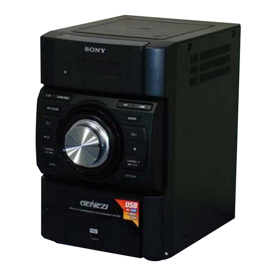
SERVICE MANUAL
Ver. 1.0 2010.06
• HCD-EC59 is the amplifi er, USB, CD player and
tuner section in MHC-EC59.
• MPEG Layer-3 audio coding technology and patents licensed from Fraunhofer IIS and Thomson.
• Windows Media is either a registered trademark or trademark of Microsoft Corporation in the
United States and/or other countries.
• This product is protected by certain intellectual property rights of Microsoft Corporation. Use or
distribution of such technology outside of this product is prohibited without a license from Micro-
soft or an authorized Microsoft subsidiary.
Main unit
Amplifier section
The following measured at AC 127 V, 60 Hz
(Mexican model)
The following measured at AC 220 V,
50/60 Hz (Argentine model)
The following measured at AC 120 V, 220 V,
240 V, 50/60 Hz (Other models)
Power output (rated):
25 W + 25 W (at 6 Ω, 1 kHz, 1%
THD)
RMS output power (reference):
60 W + 60 W (per channel at 6 Ω,
1 kHz)
Inputs
PC IN (stereo mini jack):
Sensitivity 800 mV, impedance
22 kilohms
Outputs
PHONES (stereo mini jack):
accepts headphones with an
impedance of 8 Ω or more
SPEAKERS: impedance: 6 Ω
USB section
Supported bit rate:
MP3 (MPEG 1 Audio Layer-3):
32 kbps – 320 kbps, VBR
WMA: 48 kbps – 192 kbps
AAC: 48 kbps – 320 kbps
Sampling frequencies:
MP3 (MPEG 1 Audio Layer-3):
32/44.1/48 kHz
WMA: 44.1 kHz
AAC: 44.1 kHz
(USB) port:
Maximum current:
500 mA
Sony Corporation
9-889-885-01
2010F05-1
Audio&Video Business Group
©
2010.06
Published by Sony Techno Create Corporation
HCD-EC59
Model Name Using Similar Mechanism
Base Unit Name
Optical Pick-up Block Name
SPECIFICATIONS
CD player section
System:
Compact disc and digital audio
system
Laser Diode Properties
Emission Duration: Continuous
Laser Output*: Less than 44.6μW
* This output is the value
measurement at a distance of
200mm from the objective lens
surface on the Optical Pick-up Block
with 7mm aperture.
Frequency response: 20 Hz – 20 kHz
Signal-to-noise ratio: More than 90 dB
Dynamic range: More than 88 dB
Tuner section
FM stereo, FM/AM superheterodyne tuner
Antenna:
FM lead antenna
AM loop antenna
FM tuner section:
Tuning range:
87.5 MHz – 108.0 MHz (50 kHz step)
Intermediate frequency: 225 kHz
AM tuner section:
Tuning range
Latin American models:
530 kHz – 1,710 kHz (10 kHz step)
531 kHz – 1,710 kHz (9 kHz step)
Other models:
531 kHz – 1,602 kHz (9 kHz step)
530 kHz – 1,610 kHz (10 kHz step)
Intermediate frequency: 53 kHz
General
Power requirements
Mexican model:
AC 127 V, 60 Hz
Argentine model:
AC 220 V, 50/60 Hz
Other models:
AC 120 V, 220 V or 230 V 240 V,
50/60 Hz, adjustable with voltage
selector
Power consumption: 85 W
(0.5 Wat the Power Saving Mode)
Dimensions (W/H/D) (excl. speakers)
Approx. 200 mm × 306 mm ×
305 mm
Mass (excl. speakers): Approx. 3.8 kg
Design and specifications are subject to
change without notice.
Standby power consumption: 0.5 W
Halogenated flame retardants are not used
in the certain printed wiring boards.
COMPACT DISC RECEIVER
E Model
HCD-EX6/EX6T
BU-D1BD74UR
DA11MMVGP
Advertisement
Table of Contents

Subscribe to Our Youtube Channel
Related Manuals for Sony HCD-EC59


Summary of Contents for Sony HCD-EC59
- Page 1 SERVICE MANUAL E Model Ver. 1.0 2010.06 • HCD-EC59 is the amplifi er, USB, CD player and tuner section in MHC-EC59. • MPEG Layer-3 audio coding technology and patents licensed from Fraunhofer IIS and Thomson. Model Name Using Similar Mechanism HCD-EX6/EX6T •...
-
Page 2: Table Of Contents
COMPONENTS IDENTIFIED BY MARK 0 OR DOTTED LINE WITH MARK 0 ON THE SCHEMATIC DIAGRAMS AND IN THE PARTS LIST ARE CRITICAL TO SAFE OPERATION. REPLACE THESE COMPONENTS WITH SONY PARTS WHOSE PART NUMBERS APPEAR AS SHOWN IN THIS MANUAL OR IN SUPPLEMENTS PUBLISHED BY SONY. -
Page 3: Servicing Notes
HCD-EC59 SECTION 1 SERVICING NOTES MODEL IDENTIFICATION NOTES ON HANDLING THE OPTICAL PICK-UP - Back Panel - BLOCK OR BASE UNIT The laser diode in the optical pick-up block may suffer electro- Model static break-down because of the potential difference generated by Number the charged electrostatic load, etc. - Page 4 HCD-EC59 CAPACITOR ELECTRICAL DISCHARGE PROCESSING When checking the board, the electrical discharge is necessary for the electric shock prevention. Connect the resistors referring to the fi gure below. • MAIN board (C622, C626) Both ends of respective capacitors. – MAIN Board (Conductor Side) –...
- Page 5 HCD-EC59 PT-SWITCH BOARD SERVICE POSITION • SIDE PANEL (R) was removed. PT-SWITCH board BD74UR BOARD SERVICE POSITION • SIDE PANEL (L) and (R) are removed, and the set is laid. top panel block BD74UR board...
-
Page 6: Disassembly
HCD-EC59 SECTION 2 DISASSEMBLY • This set can be disassembled in the order shown below. 2-1. DISASSEMBLY FLOW 2-2. SIDE PANEL (L)/(R) (Page 7) 2-3. TOP PANEL ASSY (Page 7) 2-4. FRONT PANEL BLOCK 2-6. MAIN BOARD 2-7. BASE UNIT... -
Page 7: Side Panel (L)/(R)
HCD-EC59 Note: Follow the disassembly procedure in the numerical order given. 2-2. SIDE PANEL (L)/(R) 4 two claws 2 two screws (BVTP3 4 two claws 1 three screws (case 3 TP2) 5 side panel (L) 2 two screws (BVTP3 1 three screws... -
Page 8: Front Panel Block
HCD-EC59 2-4. FRONT PANEL BLOCK 3 screw (BVTP3 4 lead wire (from USB board) 1 flexible flat cable (25 core) (CN607) 6 claw 2 flexible flat cable (9 core) (CN605) 8 front panel block 6 claw 5 three screws (BVTT3 2-5. -
Page 9: Main Board
HCD-EC59 2-6. MAIN BOARD 5 flexible flat cable (5 core) 6 connector (CN603) 0 MAIN board (CN633) 7 fan motor connector (CN601) 8 screw (BVTP3 4 connector (CN604) 8 two screws (BVTP3 8 screw (BVTP3 9 lead wire (from USB board) -
Page 10: Base Unit (Bu-D1Bd74Ur)
HCD-EC59 2-7. BASE UNIT (BU-D1BD74UR) Note 1: This illustration sees the top panel assy from base unit side. 4 two insulators (blue) 1 four floating screws (PTPWHM2.6) 7 base unit 3 two insulators (BU-D1BD74UR) (gray) 5 four claws Note 2: Four claws might be fixed by bond. -
Page 11: Test Mode
HCD-EC59 SECTION 3 TEST MODE COLD RESET CHANGE-OVER THE AM TUNING INTERVAL The cold reset clears all data including preset data stored in the The AM tuning interval can be changed over 9 kHz or 10 kHz. memory to initial conditions. Execute this mode when returning Procedure: the set to the customer. - Page 12 HCD-EC59 CD FACTORY MODE Note 1: Do not enter the this mode while any other test mode is in prog- ress. Note 2: Do not enter any other test mode while the this mode is in prog- ress. Procedure: 1. Press the [ ] button to turn the power on.
-
Page 13: Electrical Checks
HCD-EC59 SECTION 4 ELECTRICAL CHECKS CD SECTION 0 dB = 1 μV TUNER SECTION Note: FM AUTO STOP CHECK 1. CD Block is basically constructed to operate without adjustment. signal 2. Use YEDS-18 disc (Part No. 3-702-101-01) unless otherwise indicat- generator 3. -
Page 14: Diagrams
HCD-EC59 SECTION 5 DIAGRAMS THIS NOTE IS COMMON FOR PRINTED WIRING BOARDS AND SCHEMATIC DIAGRAMS. (In addition to this, the necessary note is printed in each block.) For Printed Wiring Boards. For Schematic Diagrams. Note: Note: • X : parts extracted from the component side. - Page 15 HCD-EC59 • Circuit Boards Location BD74UR board MAIN board REG board PANEL board JACK board PT-SWITCH board USB board 2CH AMP board USB-JACK board...
- Page 16 HCD-EC59 • IC Pin Function Description USB BOARD IC901 LC87F1JJ2AU-SQFP-H (USB CONTROLLER) Pin No. Pin Name Description Not used Reset signal input from the system controller “L”: reset Not used Not used VSS1 Ground terminal Main system clock input terminal (12 MHz)
- Page 17 HCD-EC59 PANEL BOARD IC301 MB90F831PF-G-SPE1 (SYSTEM CONTROLLER) Pin No. Pin Name Description Pin No. Pin Name Description SEG32 Segment drive signal output to the liquid crystal display Power supply terminal (+3.3V) O-SP-RELAY-ON Relay drive signal output terminal (for speaker) Ground terminal...
-
Page 18: Printed Wiring Board - Cd Section
HCD-EC59 5-1. PRINTED WIRING BOARD - CD Section - • See page 15 for Circuit Boards Location. • : Uses unleaded solder. BD74UR BOARD BD74UR BOARD (CONDUCTOR SIDE) (COMPONENT SIDE) M401 (SPINDLE) C301 CL119 CL419 CL117 S001 (LIMIT) CL420 SL304... -
Page 19: Schematic Diagram - Cd Section
HCD-EC59 5-2. SCHEMATIC DIAGRAM - CD Section - • See page 24 for Waveforms. • See page 30 for IC Block Diagrams. BD74UR BOARD C132 R417 C133 C131 C130 C127 R129 R131 X101 16.934MHz CN201 C201 VREF CL212 CL213 C203... -
Page 20: Printed Wiring Board - Usb Section
HCD-EC59 5-3. PRINTED WIRING BOARD - USB Section - • See page 15 for Circuit Boards Location. • : Uses unleaded solder. (Page 26) PANEL BOARD CN451 USB BOARD (SIDE A) USB BOARD (SIDE B) CL911 CL920 CL912 CL909 CL921... -
Page 21: Schematic Diagram - Usb Section
HCD-EC59 5-4. SCHEMATIC DIAGRAM - USB Section - • See page 24 for Waveforms. • See page 16 for IC Pin Function Descriptions. USB BOARD CN903 VBUSGND R951 CL934 USB-JACK C950 BOARD CL935 R952 CN561 VBUS5V (Page 25) R953 R954... -
Page 22: Printed Wiring Boards - Main Section
HCD-EC59 5-5. PRINTED WIRING BOARDS - MAIN Section - • See page 15 for Circuit Boards Location. • : Uses unleaded solder. MAIN BOARD D801 FL801 TP804 CN801 ANTENNA JR602 JR601 C815 R811 IC801 FM/AM C816 R809 C859 L802 L803... -
Page 23: Schematic Diagram - Main Section
HCD-EC59 5-6. SCHEMATIC DIAGRAM - MAIN Section - • See page 24 for Waveforms. • See page 30 for IC Block Diagrams. MAIN BOARD CN801 R809 C859 C820 R807 X801 TP805 180k 32.768kHz ANTENNA R698 R705 R701 R702 C699 C700... -
Page 24: Printed Wiring Boards - 2Ch Amp/Usb-Jack/Jack Boards
HCD-EC59 • Waveforms 5-7. PRINTED WIRING BOARDS - 2CH AMP/USB-JACK/JACK Boards - • See page 15 for Circuit Boards Location. • : Uses unleaded solder. – BD74UR Board – – USB Board – – PANEL Board – IC101 2 (RFOUT) -
Page 25: Schematic Diagram
HCD-EC59 5-8. SCHEMATIC DIAGRAM - 2H AMP/USB-JACK/JACK Boards - 2CH AMP BOARD USB-JACK BOARD IC102 CN561 2CH POWER AMP FB561 TP562 IC102 R562 CN560 +PRE SUB GND VBUS5V STK433-040 TP561 TP560 BOARD TP559 R561 C565 C561 CN903 VBUSGND (Page 21) -
Page 26: Printed Wiring Board - Panel Board
HCD-EC59 5-9. PRINTED WIRING BOARD - PANEL Board - • See page 15 for Circuit Boards Location. • : Uses unleaded solder. PANEL BOARD R498 JW304 JW305 R328 LCD301 R497 JW309 X302 R402 C342 LIQUID CRYSTAL DISPLAY Q301 R326 C497... -
Page 27: 5-10. Schematic Diagram - Panel Board
HCD-EC59 5-10. SCHEMATIC DIAGRAM - PANEL Board - • See page 24 for Waveforms. • See page 16 for IC Pin Function Descriptions. PANEL BOARD SW305 CD LID OPEN/CLOSE W305 DETECT X302 6MHz TP341 C306 C341 C321 C342 CD-OPEN/CLOSE 1000p 6.3V... -
Page 28: 5-11. Printed Wiring Board - Pt-Switch Board
HCD-EC59 5-11. PRINTED WIRING BOARD - PT-SWITCH Board - • See page 15 for Circuit Boards Location. • : Uses unleaded solder. (AC IN) PT-SWITCH BOARD (MX) (EXCEPT MX) RY051 RY052 C051 JW009 JW008 JW019 JW020 (EXCEPT MX) (MX) JW018... -
Page 29: 5-12. Schematic Diagram - Pt-Switch Board
HCD-EC59 5-12. SCHEMATIC DIAGRAM - PT-SWITCH Board - PT-SWITCH BOARD (EXCEPT MX) C051 (MX) RY051 RY052 PT051 JW008 JW009 SUB POWER TRANSFORMER JW007 JW004 (E2, E4, E51) VOLTAGE S051 SELECTOR JW006 120V CN051 220V LIVE (AC IN) NEUTRAL 230-240V JW011... - Page 30 HCD-EC59 • IC Block Diagrams – BD74UR Board – – MAIN Board – IC301 BA5826HFP-E2 IC601 BD3491FS-SE2 IC101 LC786950T-US-H 32 SDA VO1(–) 31 SCL D.BUFF VO4(–) VO1(+) D.BUFF D.BUFF LEVEL INPUT SHIFT VO4(+) 30 FIL CLOCK SELECTOR INPUT EFMIN 1...
- Page 31 HCD-EC59 IC701 NJM2368V (TE2) VOLTAGE REFERENCE 30 A L. O UNDERVOLTAGE LOCKOUT S. C. P ERROR IC801 LV23401V-TLM-H OSC CAP REFERENCE LOCAL POWER STATE DIVIDER OSCILLATOR MANAGEMENT MACHINE TUNING AGC DET SYSTEM SD OUT ST OUT BAND-PASS STEREO STEREO AUDIO...
-
Page 32: Exploded Views
HCD-EC59 SECTION 6 EXPLODED VIEWS Note: • -XX and -X mean standardized parts, so • Color Indication of Appearance Parts Ex- The components identifi ed by mark 0 they may have some difference from the ample: or dotted line with mark 0 are critical for original one. -
Page 33: Front Panel Section
HCD-EC59 6-2. FRONT PANEL SECTION not supplied (JACK HOLD board) not supplied (JACK board) supplied supplied (USB board) not supplied (PANEL board) not supplied not supplied (USB-JACK board) Ref. No. Part No. Description Remark Ref. No. Part No. Description Remark... -
Page 34: Chassis Section
HCD-EC59 6-3. CHASSIS SECTION M601 not supplied not supplied (REG board) not supplied (AC HOLD board) not supplied PT054 supplied not supplied (2CH AMP board) not supplied (PT-SWITCH board) not supplied not supplied (CORD HOLD board) Ref. No. Part No. -
Page 35: Top Panel Section
HCD-EC59 6-4. TOP PANEL SECTION not supplied SW305 (including sled motor (M402), spindle motor (M401)) not supplied (spindle motor (M401)) not supplied not supplied not supplied (sled motor (M402)) S001 Ref. No. Part No. Description Remark Ref. No. Part No. -
Page 36: Electrical Parts List
HCD-EC59 SECTION 7 2CH AMP BD74UR ELECTRICAL PARTS LIST Note: • Due to standardization, replacements in • CAPACITORS When indicating parts by reference num- the parts list may be different from the uF: μF ber, please include the board name. - Page 37 HCD-EC59 BD74UR JACK Ref. No. Part No. Description Remark Ref. No. Part No. Description Remark C122 1-164-156-11 CERAMIC CHIP 0.1uF C123 1-164-156-11 CERAMIC CHIP 0.1uF R118 1-216-809-11 METAL CHIP 1/10W R120 1-216-833-11 METAL CHIP 1/10W C124 1-128-995-21 ELECT CHIP 100uF...
- Page 38 HCD-EC59 MAIN Ref. No. Part No. Description Remark Ref. No. Part No. Description Remark A-1772-508-A MAIN BOARD, COMPLETE (E2, E51, AR) C699 1-162-964-11 CERAMIC CHIP 0.001uF A-1772-509-A MAIN BOARD, COMPLETE (MX) C700 1-162-964-11 CERAMIC CHIP 0.001uF A-1787-869-A MAIN BOARD, COMPLETE (E4)
- Page 39 HCD-EC59 MAIN Ref. No. Part No. Description Remark Ref. No. Part No. Description Remark D611 6-501-582-01 DIODE 1N4002-A2 < RESISTOR > D612 6-501-582-01 DIODE 1N4002-A2 R609 1-216-829-11 METAL CHIP 4.7K 1/10W D614 6-501-817-01 DIODE MA2J1110GLS0 R610 1-216-829-11 METAL CHIP 4.7K...
- Page 40 HCD-EC59 MAIN PANEL Ref. No. Part No. Description Remark Ref. No. Part No. Description Remark R692 1-216-829-11 METAL CHIP 4.7K 1/10W R801 1-216-821-11 METAL CHIP 1/10W R693 1-216-821-11 METAL CHIP 1/10W R802 1-216-821-11 METAL CHIP 1/10W R697 1-216-864-11 SHORT CHIP...
- Page 41 HCD-EC59 PANEL Ref. No. Part No. Description Remark Ref. No. Part No. Description Remark < CONNECTOR > R329 1-216-825-11 METAL CHIP 2.2K 1/10W R330 1-216-819-11 METAL CHIP 1/10W CN301 1-784-747-11 CONNECTOR, FFC 25P R331 1-216-845-11 METAL CHIP 100K 1/10W CN305...
- Page 42 HCD-EC59 PANEL PT-SWITCH Ref. No. Part No. Description Remark Ref. No. Part No. Description Remark R475 1-216-826-11 METAL CHIP 2.7K 1/10W < TRANSFORMER > R476 1-216-828-11 METAL CHIP 3.9K 1/10W 0 PT051 1-445-105-11 TRANSFORMER, POWER R480 1-216-833-11 METAL CHIP 1/10W...
- Page 43 HCD-EC59 USB-JACK Ref. No. Part No. Description Remark Ref. No. Part No. Description Remark < RESISTOR > MISCELLANEOUS ************** R900 1-216-864-11 SHORT CHIP R901 1-216-809-11 METAL CHIP 1/10W 1-832-814-21 CABLE, FLEXIBLE FLAT (9 CORE) R902 1-216-809-11 METAL CHIP 1/10W 1-832-635-21...
-
Page 44: Revision History
HCD-EC59 REVISION HISTORY Checking the version allows you to jump to the revised page. Also, clicking the version at the top of the revised page allows you to jump to the next revised page. Ver. Date Description of Revision 2010.06...
Need help?
Do you have a question about the HCD-EC59 and is the answer not in the manual?
Questions and answers