Table of Contents
Advertisement
SERVICE MANUAL
HCD-CP2A is the Amplifier, CD player,
Tape Deck and Tuner section in
CMT-CP2WA.
Dolby noise reduction manufactured under license
from Dolby Laboratories Licensing Corporation.
"DOLBY" and the double-D symbol ; are trade-
marks of Dolby Laboratories Licensing Corporation.
Amplifier section
European and Australian models:
DIN power output (rated): 30 + 30 W
Continuous RMS power output (reference):
Music power output (reference):
Other models:
The following measured at 230 V AC, 60 Hz
DIN power output (rated): 30 + 30 W
Continuous RMS power output (reference):
The following measured at 220 V AC, 60 Hz
DIN power output (rated): 28 + 28 W
Continuous RMS power output (reference):
Inputs
MD IN (phono jacks):
VIDEO IN (phono jacks): Sensitivity 250 mV, impedance
Outputs
LINE OUT (phono jacks): Sensitivity 250 mV, impedance
OPTICAL DIGITAL OUT CD:
PHONES (stereo phone jack):
SPEAKER:
CD
Section
TAPE
Section
SPECIFICATIONS
CD player section
System
(6 ohms at 1 kHz, DIN)
Laser
35 + 35 W
(6 ohms at 1 kHz, 10% THD)
Laser output
130 W
Wavelength
(6 ohms at 1 kHz, DIN)
Frequency response
35 + 35 W
(6 ohms at 1 kHz, 10% THD)
Tape player section
Recording system
(6 ohms at 1 kHz, DIN)
Frequency response (DOLBY NR OFF)
33 + 33 W
(6 ohms at 1 kHz, 10% THD)
Sensitivity 500 mV, impedance
47 kilohms
47 kilohms
1 kilohm
Optical
Accepts headphones with an
impedance of 8 ohms or more
Active speaker system, 6 ohms
HCD-CP2A
Australian Model
Model Name Using Similar Mechanism
CD Mechanism Type
Base Unit Name
Optical Pick-up Name
Model Name Using Similar Mechanism
Tape Transport Mechanism Type
Compact disc and digital audio
system
Semiconductor laser
(λ = 780 nm)
Emission duration: continuous
MAX 44.6 µ W*
* This output is the value
measured at a distance of
200 mm from the objective
lens surface on the Optical
Pick-up Block with 7 mm
aperture.
780 - 790 nm
20 Hz - 20 kHz (±0.5 dB)
4-track 2-channel stereo
50 - 13,000 Hz (±3 dB), using a
Sony TYPE I cassette
50 - 14,000 Hz (±3 dB),
using a Sony TYPE II cassette
COMPACT DISC DECK RECEIVER
AEP Model
UK Model
E Model
NEW
CDM55D-K5BD41
BU-K5BD41
KSM-213CKP/K1N
NEW
CMBL6Z112
– Continued on next page –
Advertisement
Table of Contents

Subscribe to Our Youtube Channel
Related Manuals for Sony HCD-CP2A


Summary of Contents for Sony HCD-CP2A
-
Page 1: Specifications
HCD-CP2A SERVICE MANUAL AEP Model UK Model E Model Australian Model HCD-CP2A is the Amplifier, CD player, Tape Deck and Tuner section in CMT-CP2WA. Dolby noise reduction manufactured under license Model Name Using Similar Mechanism from Dolby Laboratories Licensing Corporation. -
Page 2: Table Of Contents
LINE WITH MARK 0 ON THE SCHEMATIC DIAGRAMS AND IN THE PARTS LIST ARE CRITICAL TO SAFE OPERATION. REPLACE THESE COMPONENTS WITH SONY PARTS WHOSE PART NUMBERS APPEAR AS SHOWN IN THIS MANUAL OR IN SUPPLEMENTS PUB- LISHED BY SONY. -
Page 3: Servicing Notes
SECTION 1 SERVICING NOTES Notes on chip component replacement NOTES ON HANDLING THE OPTICAL PICK-UP • Never reuse a disconnected chip component. BLOCK OR BASE UNIT • Notice that the minus side of a tantalum capacitor may be dam- The laser diode in the optical pick-up block may suffer electro- aged by heat. -
Page 4: General
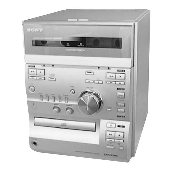
SECTION 2 GENERAL • LOCATION OF CONTROLS – Front View – 1 TAPE A deck 2 TAPE B deck 3 Liquid crystal display 4 TAPE B Y button 5 TAPE B x button 6 TAPE B M button 7 TAPE B m button 8 VOLUME knob 9 TREBLE knob 0 BASS knob... -
Page 5: Setting The Time
This section is extracted from instruction manual. -
Page 6: Disassembly
SECTION 3 DISASSEMBLY Note: Follow the disassembly procedure in the numerical order given. COVER (UPPER) 3 cover (upper) 1 two case screws 2 six screws (BTP3 × 8) 1 two case screws FRONT PANEL ASS’Y 2 two connectors (CN805, 808) 1 wire (flat type)(17 core)(22 cm) 2 connector (CN311) - Page 7 TAPE MECHANISM DECK SECTION 2 Push these buttons. 1 six screws (BTP3 × 8) 3 tape mechanism deck section CD MECHANISM DECK (CDM55D-K5BD41) 2 connector (CN304) 3 screw (BTP3 × 8) 1 wire (flat type)(19 core) (CN301) 4 CD mechanism deck (CDM55D-K5BD41)
- Page 8 BASE UNIT (BU-K5BD41) 1 floating screw (PTPWHM2.6) 2 base unit (BU-K5BD41) TRAY, LOADING BOARD 2 belt (CDM55) 1 Rotate the gear(B) in the direction of arrow A. 3 Pull the tray pushing B. 5 LOADING board 4 two screws (BTP2.6 × 6)
- Page 9 CAM (CDM55) 3 spacer (55) 4 pulley (LDG) 6 gear (B) 5 gear (A) 1 torsion spring 7 roller 8 cam (CDM55) 2 lever (SW)
-
Page 10: Test Mode
SECTION 4 TEST MODE [Tape Deck Aging Mode] [MC Cold Reset] • The cold reset clears all data including preset data stored in the This mode can be used for operation check of tape deck section. RAM to initial conditions. Execute this mode when returning the set to the customer. -
Page 11: Mechanical Adjustments
SECTION 5 SECTION 6 MECHANICAL ADJUSTMENTS ELECTRICAL ADJUSTMENTS PRECAUTION TAPE DECK SECTION 0 dB=0.775 V 1. Clean the following parts with a denatured-alcohol-moistened 1. Demagnetize the record/playback head with a head demagne- swab: record/playback heads pinch rollers tizer. (Do not bring the head demagnetizer close to the erase head) erase head rubber belts... - Page 12 DECK A DECK B 1. Mode: Playback (FWD) Tape Speed Check 2. Turn the adjustment screw and check output peaks. If the peaks Procedure: do not match for L-CH and R-CH, turn the adjustment screw Mode: Playback (FWD) so that outputs match within 1dB of peak. test tape WS-48B frequency counter...
- Page 13 DECK B Record bias Current Adjustment Adjustment and Checking Location: Procedure: – MAIN BOARD (Conductor Side) – 1. Mode: Record Pin rd (L-CH) of IC306 on the MAIN board. Pin th (R-CH) of IC306 on the MAIN board. 1) 315 Hz ...
-
Page 14: Cd Section
CD SECTION – CD BOARD (Conductor Side) – Note: CD Block is basically constructed to operate without adjustment. Use YEDS-18 disc (3-702-101-01) unless otherwise indicated. Use an oscilloscope with more than 10 MΩ impedance. Clean the object lens by an applicator with neutral detergent when the signal level is low than specified value with the following checks. -
Page 15: Diagrams
HCD-CP2A SECTION 7 DIAGRAMS 7-1. NOTE FOR PRINTED WIRING BOARDS AND SCHEMATIC DIAGRAMS • Circuit Boards Location Note on Printed Wiring Boards: Note on Schematic Diagram: • X : parts extracted from the component side. • All capacitors are in µF unless otherwise noted. pF: µµF •... -
Page 16: Printed Wiring Board - Cd Board
HCD-CP2A 7-2. PRINTED WIRING BOARD – CD Board – • See page 15 for Circuit Boards Location. • Semiconductor Location Ref. No. Location IC101 IC102 IC103 Q101 (Page 23) - Page 17 HCD-CP2A 7-3. SCHEMATIC DIAGRAM – CD Section – • See page 29 for Waveforms. • See page 31 for IC Block Diagrams. (Page 21) • Voltages and waveforms are dc with respect to ground under no-signal conditions. no mark : CD PLAY ∗...
-
Page 18: Printed Wiring Board - Tc Board
HCD-CP2A 7-4. PRINTED WIRING BOARD – TC Board – • See page 15 for Circuit Boards Location. (Page 23) • Semiconductor Location Ref. No. Location IC401 IC402 IC403 Q401 Q402 Q403 Q404... -
Page 19: Schematic Diagram - Tc Section
HCD-CP2A 7-5. SCHEMATIC DIAGRAM – TC Section – • See page 29 for Waveforms. (Page 20) • Voltages and waveforms are dc with respect to ground under no-signal conditions. no mark : TAPE PLAY 〈〈 〉〉 : TAPE REC... -
Page 20: Schematic Diagram - Cd Section
HCD-CP2A 7-6. SCHEMATIC DIAGRAM – MAIN Section (1/3) – (Page 21) (Page 19) (Page 22) • Voltages and waveforms are dc with respect to ground under no-signal (detuned) conditions. no mark : FM ) : CD PLAY ] : TAPE PLAY 〈〈... -
Page 21: Schematic Diagram - Main Section (2/3)
HCD-CP2A 7-7. SCHEMATIC DIAGRAM – MAIN Section (2/3) – • See page 31 for IC Block Diagrams. (Page 25) (Page 28) (Page 20) (Page 22) (Page 22) (Page 22) (Page 22) (Page 22) (Page 17) • Voltages and waveforms are dc with respect to ground under no-signal (detuned) conditions. -
Page 22: Schematic Diagram - Main Section (3/3)
HCD-CP2A 7-8. SCHEMATIC DIAGRAM – MAIN Section (3/3) – • See page 29 for Waveforms. • See page 31 for IC Block Diagrams. (Page 21) (Page 21) (Page 21) (Page 21) (Page 20) (Page 27) (Page 21) • Voltages and waveforms are dc with respect to ground under no-signal (detuned) conditions. -
Page 23: Printed Wiring Board - Main Board
HCD-CP2A 7-9. PRINTED WIRING BOARD – MAIN Board – • See page 15 for Circuit Boards Location. • Semiconductor Location Ref. No. Location Ref. No. Location IC803 D301 D302 D303 Q101 C-10 Q102 D304 D305 Q103 D306 H-10 Q106 D307... -
Page 24: Printed Wiring Board - Loading Board
HCD-CP2A 7-10. PRINTED WIRING BOARD – LOADING Board – • See page 15 for Circuit Boards Location. 7-12. PRINTED WIRING BOARDS – AMP/HEADPHONE Boards – • See page 15 for Circuit Boards Location. • Semiconductor Location Ref. No. Location IC101... -
Page 25: Schematic Diagram - Amp Section
HCD-CP2A 7-13. SCHEMATIC DIAGRAM – AMP Section – • See page 31 for IC Block Diagrams. (Page 28) (Page 21) • Voltages and waveforms are dc with respect to ground under no-signal (detuned) conditions. no mark : FM... -
Page 26: Printed Wiring Board - Control Board
HCD-CP2A 7-14. PRINTED WIRING BOARD – CONTROL Board – • See page 15 for Circuit Boards Location. • Semiconductor Location Ref. No. Location D810 D811 D812 D813 D814 D817 D820 D821 D822 D823 IC804 Q807 Q808 Q809 Q810 Q811 Q812... -
Page 27: Schematic Diagram - Control Section
HCD-CP2A 7-15. SCHEMATIC DIAGRAM – CONTROL Section – (Page 22) • Voltages and waveforms are dc with respect to ground under no-signal (detuned) conditions. no mark : FM... -
Page 28: Printed Wiring Board - Power Board
HCD-CP2A 7-16. PRINTED WIRING BOARD – POWER Board – • See page 15 for Circuit Boards Location. 7-17. SCHEMATIC DIAGRAM – POWER Section – (Page 24) (Page 23) (Page 25) (Page 21) The components identified by mark 0 or dotted •... - Page 29 • Waveforms – CD Board – – TC Board – 1 IC103 qh (RFO) (CD Play Mode) 6 IC101 w; (SCOR) (CD Play Mode) 1 Q402 collector (REC Mode) 1.2 ±0.1 Vp-p 14.8 Vp-p 12 µs 13.2 ms 2 IC103 qf (FE) (CD Play Mode) 7 IC101 yh (XTAI) 2 Q402 base (REC Mode) Approx.
- Page 30 – MAIN Board – 1 IC802 wh (C/D) 6 IC803 qd (XI) (FM Mode) (AEP, UK only) 2.4 Vp-p 5 Vp-p 4.332 MHz 34 ms 2 IC802 wl (LCD-CE) 5 Vp-p 34 ms 3 IC802 ea (EXTAL1) 3.6 Vp-p 4.19 MHz 4 IC802 eg (TEX) 2.6 Vp-p 32.768 kHz...
- Page 31 • IC Block Diagrams – CD Board – IC101 CXD2587Q ERROR DIGITAL CORRECTOR DIGITAL ASYMMETRY CORRECTION OPERATIONAL LRCK AMPLIFIER ANALOG SWITCH PCMD INTERFACE DEMODULATOR CONVERTER EMPH XVDD XTAI TIMING CLOCK XTAO LOGIC XTSL GENERATOR XVSS TES1 AVDD1 TEST AOUT1 SERVO DSP PWM GENERATOR AIN1 FRDR...
- Page 32 IC103 CXA2568M-T6 HOLD APC PD AMP LC/PD APC LD AMP – LD ON – – – HOLD SW AGC CONT AGC VTH 50µA RF BOT – – – – RFTC RF SUMMING AMP RF EQ AMP RF I RF O –...
-
Page 33: Main Board
– MAIN Board – IC301 TDA7439 IC309 KA3082 DRIVER OUT 26 25 24 23 22 21 20 19 PRE DRIVER VOLUME VOLUME LOGIC SWITCH TREBLE TREBLE 8 9 10 MIDDLE MIDDLE BASS BASS SPEAKER SPEAKER ATTENUATOR ATTENUATOR IIC BUS DECODER & LATCH VREF GAIN AMP... -
Page 34: Amp Board
IC803 BU1924F-E2 12 11 10 CLOCK TEST PLL 57kHz RDS/ARI 1187.5Hz COMPARATOR 8th SWITCHED BIPHASE CAPACITOR DECODER FILTER DEFFERENTIAL ANTI-ALIASING DECODER FILTER – AMP Board – IC101, 201 TDA7296 THERMAL BIPOLAR SHUTDOWN TRANSCONDACTANCE INPUT STAGE MOS GAIN & SHORT – LEVEL SHIFTING OUTPUT CIRCUIT... -
Page 35: Ic Pin Function Description
7-18. IC PIN FUNCTION DESCRIPTION • MAIN BOARD IC802 CXP84332-224Q (SYSTEM CONTROLLER) Pin No. Pin Name Description Deck-A/B selection signal output to the HA12215F (IC306) “L”: deck-A, “H”: deck-B TREBLE A Jog dial pulse input from the rotary encoder (RV803 TREBLE) (A phase input) High speed dubbing control signal output to the HA12215F (IC306) REC (DUB/HI-DUB) C-XRST... - Page 36 Pin No. Pin Name Description Key input terminal (A/D input) S808 to S815 (CD x/u, TUNING MODE, REPEAT, PLAY KEY2 MODE,CD > M/. m/Z keys input) Key input terminal (A/D input) KEY3 S817 to S823 (DSG, VIDEO, MD, TAPE, CD, TUNER, I/1 keys input) Key input terminal (A/D input) KEY4 S824 to S831 (X, CD SYNC, HI-SPEED DUBBING, TAPE A M/m/x/Y keys input)
- Page 37 Pin No. Pin Name Description — Connected to power supply (+5V) AU MUTE Muting on/off control signal output terminal “H”: muting on Line muting on/off selection signal output to the HA12215F (IC306) LINE MUTE “L”: tape playback, “H”: recoding C-CLK Serial data transfer clock signal output to the CXD2587Q (IC101) C-DATA Serial data output to the CXD2587Q (IC101)
-
Page 38: Exploded Views
SECTION 8 EXPLODED VIEWS NOTE: • -XX and -X mean standardized parts, so they • Items marked “*” are not stocked since they The components identified by mark 0 or dotted line with mark may have some difference from the original are seldom required for routine service. - Page 39 (2) FRONT PANEL SECTION not supplied not supplied Ref. No. Part No. Description Remark Ref. No. Part No. Description Remark X-4952-336-1 KNOB ASSY 1-418-692-31 INDICATOR BLOCK, LED 4-229-014-01 KNOB (BASS) (DECK-A CASSETTE HOLDER BACK LIGHT) X-4952-974-1 PANEL SUB ASSY, FRONT (AEP, UK) 4-222-388-01 SPRING (CASSETTE LID) X-4953-086-1 PANEL SUB ASSY, FRONT (EA, AUS) 4-222-394-01 BRACKET (CASSETTE LID A)
- Page 40 (3) CHASSIS SECTION AEP, UK AEP, UK, CDM55D-K5BD41 T901 supplied supplied not supplied supplied not supplied The components identified by mark 0 or dotted line with mark 0 are critical for safety. Replace only with part number specified. Ref. No. Part No.
- Page 41 (4) CD MECHANISM DECK SECTION (CDM55D-K5BD41) M901 BU-K5BD41 Ref. No. Part No. Description Remark Ref. No. Part No. Description Remark 4-224-894-01 TRAY 4-221-815-01 ROLLER 4-220-229-01 LEVER (SW) 4-225-884-01 CHASSIS (55D) 4-220-239-01 SPRING, TORSION X-4952-811-1 PULLEY (AT) ASSY 4-221-816-01 BELT (CDM55) 4-220-951-02 SHEET (KH) 4-220-234-01 PULLEY (LDG) 4-985-672-01 SCREW (+PTPWHM2.6), FLOATING...
- Page 42 (5) BASE UNIT SECTION (BU-K5BD41) The components identified by mark 0 or dotted line with mark 0 are critical for safety. Replace only with part number specified. Ref. No. Part No. Description Remark Ref. No. Part No. Description Remark 4-985-672-01 SCREW (+PTPWHM2.6), FLOATING 1-791-495-11 WIRE, PARALLEL (FFC) (16 CORE) 4-229-005-01 INSULATOR 4-229-004-01 SPRING, COMPRESSION...
-
Page 43: Electrical Parts List
SECTION 9 ELECTRICAL PARTS LIST NOTE: • Due to standardization, replacements in the • Items marked “*” are not stocked since they The components identified by mark 0 or dotted line with mark parts list may be different from the parts speci- are seldom required for routine service. - Page 44 Ref. No. Part No. Description Remark Ref. No. Part No. Description Remark R303 1-216-017-00 RES-CHIP 1/10W C171 1-163-009-11 CERAMIC CHIP 0.001uF R310 1-216-017-00 RES-CHIP 1/10W C172 1-163-123-00 CERAMIC CHIP 180PF R334 1-216-065-00 RES-CHIP 4.7K 1/10W C181 1-163-009-11 CERAMIC CHIP 0.001uF R335 1-216-073-00 METAL CHIP 1/10W...
- Page 45 CONTROL Ref. No. Part No. Description Remark Ref. No. Part No. Description Remark R143 1-216-103-00 METAL CHIP 180K 1/10W JR651 1-216-296-00 SHORT R144 1-216-103-00 METAL CHIP 180K 1/10W JR652 1-216-296-00 SHORT R147 1-216-069-00 METAL CHIP 6.8K 1/10W R148 1-216-001-00 METAL CHIP 1/10W <...
- Page 46 CONTROL HEADPHONE LOADING MAIN Ref. No. Part No. Description Remark Ref. No. Part No. Description Remark R847 1-216-065-00 RES-CHIP 4.7K 1/10W < COIL > R848 1-216-065-00 RES-CHIP 4.7K 1/10W R849 1-216-065-00 RES-CHIP 4.7K 1/10W L102 1-410-993-42 INDUCTOR CHIP 1uH L202 1-410-993-42 INDUCTOR CHIP 1uH R851 1-216-073-00 METAL CHIP...
- Page 47 MAIN Ref. No. Part No. Description Remark Ref. No. Part No. Description Remark C116 1-163-005-11 CERAMIC CHIP 470PF C317 1-164-004-11 CERAMIC CHIP 0.1uF C318 1-163-021-11 CERAMIC CHIP 0.01uF C117 1-163-005-11 CERAMIC CHIP 470PF C319 1-163-021-11 CERAMIC CHIP 0.01uF C118 1-163-005-11 CERAMIC CHIP 470PF C320 1-126-941-11 ELECT...
- Page 48 MAIN Ref. No. Part No. Description Remark Ref. No. Part No. Description Remark C817 1-163-003-11 CERAMIC CHIP 330PF < IC > (AEP, UK) IC301 8-759-585-01 IC TDA7439 C818 1-163-135-00 CERAMIC CHIP 560PF IC302 8-759-909-71 IC BA4558F (AEP, UK) IC304 8-759-646-54 IC KIA7808API C850 1-163-021-11 CERAMIC CHIP 0.01uF...
- Page 49 MAIN Ref. No. Part No. Description Remark Ref. No. Part No. Description Remark L803 1-410-993-11 INDUCTOR CHIP 1uH R108 1-216-072-00 METAL CHIP 9.1K 1/10W < JACK > R110 1-216-069-00 METAL CHIP 6.8K 1/10W R111 1-216-049-11 RES-CHIP 1/10W PJ303 1-785-926-11 JACK, PIN 6P (LINE OUT, MD IN, VIDEO IN) R112 1-216-049-11 RES-CHIP 1/10W...
- Page 50 MAIN Ref. No. Part No. Description Remark Ref. No. Part No. Description Remark R308 1-216-073-00 METAL CHIP 1/10W R526 1-216-073-00 METAL CHIP 1/10W (AEP, UK, AUS) R527 1-216-073-00 METAL CHIP 1/10W R309 1-216-049-11 RES-CHIP 1/10W R530 1-216-065-00 RES-CHIP 4.7K 1/10W (AEP, UK, AUS) R531 1-216-065-00 RES-CHIP...
- Page 51 MAIN POWER Ref. No. Part No. Description Remark Ref. No. Part No. Description Remark R634 1-216-013-00 METAL CHIP 1/10W R853 1-216-113-00 METAL CHIP 470K 1/10W R639 1-216-049-11 RES-CHIP 1/10W (AEP, UK) R640 1-216-049-11 RES-CHIP 1/10W R854 1-216-049-11 RES-CHIP 1/10W R641 1-216-049-11 RES-CHIP 1/10W (AEP, UK)
- Page 52 POWER Ref. No. Part No. Description Remark Ref. No. Part No. Description Remark D910 8-719-902-17 DIODE U15G C466 1-126-964-11 ELECT 10uF C467 1-163-021-11 CERAMIC CHIP 0.01uF D911 8-719-046-07 DIODE 2A02M C468 1-137-150-11 MYLAR 0.01uF 100V D912 8-719-046-07 DIODE 2A02M C470 1-164-182-11 CERAMIC CHIP 0.0033uF 10% D913...
- Page 53 Ref. No. Part No. Description Remark Ref. No. Part No. Description Remark R471 1-216-081-00 METAL CHIP 1/10W R472 1-216-081-00 METAL CHIP 1/10W R473 1-216-081-00 METAL CHIP 1/10W < VARIABLE RESISTOR > RV401 1-241-765-11 RES, ADJ, CARBON 22K RV402 1-241-765-11 RES, ADJ, CARBON 22K RV403 1-241-767-21 RES, ADJ, CARBON 100K RV421...
- Page 54 HCD-CP2A Sony Corporation 9-929-255-11 2000E0561-1 Audio Entertainment Group Printed in Japan C 2000. 5 Published by HA Quality Assurance Dept.
Need help?
Do you have a question about the HCD-CP2A and is the answer not in the manual?
Questions and answers