Vertex Standard VX-1210 Service Manual
Hide thumbs
Also See for VX-1210:
- Operating manual (41 pages) ,
- Alignment manual (5 pages) ,
- Service manual (4 pages)
Table of Contents
Advertisement
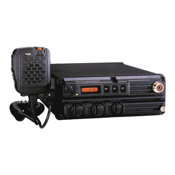
VX-1210
Service Manual
©
2001 VERTEX STANDARD CO., LTD. Printed in Japan
Introduction
This manual provides technical information necessary for servicing the VX-1210 Transceiver.
Servicing this equipment requires expertise in handling surface-mount chip components. Attempts by non-qualified persons to
service this equipment may result in permanent damage not covered by the warranty, and may be illegal in some countries.
Two PCB layout diagrams are provided for each double-sided circuit board in the transceiver. Each side of thr board is referred
to by the type of the majority of components installed on that side ("leaded" or "chip-only"). In most cases one side has only chip
components, and the other has either a mixture of both chip and leaded components (trimmers, coils, electrolytic capacitors, ICs,
etc.), or leaded components only.
While we believe the technical information in this manual to be correct, VERTEX STANDARD assumes no liability for damage
that may occur as a result of typographical or other errors that may be present. Your cooperation in pointing out any inconsistencies
in the technical information would be appreciated.
Operating Manual Reprint ............................. 2
Specifications .................................................. 10
Installation Manual Reprint ......................... 11
SEL-1200 (Option) ........................................................... 11
ATU-1210 (Option) ......................................................... 12
DSV-1200 (Option) .......................................................... 14
Exploded View & Miscellaneous Parts ...... 15
Block Diagram ................................................. 17
Interconnection Diagram .............................. 18
Circuit Description ........................................ 19
Alignment ........................................................ 21
Contents
Board Unit (Schematics, Layouts & Parts)
MAIN Unit .................................................................... 29
CNTL Unit .................................................................... 45
PA Unit .......................................................................... 57
Display Unit ................................................................. 65
Connection Unit ........................................................... 67
MIC-CONN Unit ......................................................... 68
BATT-CONN Unit ....................................................... 69
TUNER Unit (ATU-1210: Option) ............................. 71
SELCALL Unit (SEL-1200: Option) ........................... 74
VERTEX STANDARD CO., LTD.
4-8-8 Nakameguro, Meguro-Ku, Tokyo 153-8644, Japan
VERTEX STANDARD
US Headquarters
17210 Edwards Rd., Cerritos, CA 90703, U.S.A.
International Division
8350 N.W. 52nd Terrace, Suite 201, Miami, FL 33166, U.S.A.
YAESU EUROPE B.V.
P.O. Box 75525, 1118 ZN Schiphol, The Netherlands
YAESU UK LTD.
Unit 12, Sun Valley Business Park, Winnall Close
Winchester, Hampshire, SO23 0LB, U.K.
VERTEX STANDARD HK LTD.
Unit 5, 20/F., Seaview Centre, 139-141 Hoi Bun Road,
Kwun Tong, Kowloon, Hong Kong
1
Advertisement
Table of Contents

Related Manuals for Vertex Standard VX-1210


Summary of Contents for Vertex Standard VX-1210
-
Page 1: Table Of Contents
While we believe the technical information in this manual to be correct, VERTEX STANDARD assumes no liability for damage that may occur as a result of typographical or other errors that may be present. Your cooperation in pointing out any inconsistencies in the technical information would be appreciated. -
Page 2: Operating Manual Reprint
These TOGGLE switches can be customized, via program- Â VOL Knob ming by your Vertex Standard Dealer. The available fea- This control adjusts the audio volume level. Clockwise ro- tures for these switches are described on page 6. tation increases the volume level. - Page 3 Press this switch to transmit, and release it to receive. ’s loudspeaker, if the MH-50 ’s loudspeaker has Á Dummy Switch been enabled (via programming by your Vertex Standard This switch is not activated in this transceiver. dealer). Â EAR Jack Å...
- Page 4 Operating Manual Reprint PERATION Battery Charging EFORE EGIN It is necessary to charge the Battery Pack fully before its first Battery Pack Installation and Removal use. r To install the Battery Pack, insert the Battery Pack into the 1. Install the Battery Pack into the transceiver. Ensure that the battery compartment on the bottom of the radio, then secure transceiver is switched off.
- Page 5 GND terminal of the transceiver using Important Note! heavy braided cable. r If you use the VX-1210 with the optional whip an- Note: The VX-1210 can be used either with a Dipole Antenna tenna (YHA-61 or FHA-27 w/GN-1210), MUST BE...
- Page 6 PERATION UICK TART 1. Turn the transceiver on The VX-1210’s TOGGLE switch functions can be customized, by rotating the POWER via programming by the dealer. Some features may require the switch clockwise. purchase and installation of optional internal accessories. The possible TOGGLE switch programming features are illustrated at the bottom, and their functions are explained on the next page.
- Page 7 MH-50 Speaker/Microphone. shut off, or (II) to illuminate the LCD lamp until you press this switch once more (no time limit). These functions are determined via programming by your Vertex Standard Dealer.
-
Page 8: Selcall Operation
“ID1234”) will appear in the display. If a private SELCALL is the station you want to SELCALL. detected, the VX-1210 send the answer back signal to the call- 3. Press the TOGGLE switch (assigned to the “TELCALL” fea- ing station automatically before the alert ringer sounds. - Page 9 Operating Manual Reprint & O CCESSORIES PTIONS Supplied Accessories Available Options Speaker/Microphone MH-50 Internal Antenna Tuner ATU-1210 Lithium-Ion Battery Pack FNB-66LI (14.4 V, 4800 mAh) SELCALL Unit SEL-1200 Rapid Charger CD-17 Whip Antenna YHA-61 AC Adapter PA-26 Folding Whip Antenna FHA-27 (Requires GN-1210) GN-1210...
-
Page 10: Specifications
Specifications General Frequency Range: RX: 0.5 ~ 30 MHz, TX: 1.6 ~ 30 MHz Emission Modes: A1A (CW), J3E (LSB/USB), H3E (AM), F1B (AFSK) Synthesizer Steps: 10 Hz 50 W, Unbalanced Antenna Impedance: Operating Temperature Range: –30° C to +60° C Frequency Stability: ±1 ppm Power Requirements:... -
Page 11: Installation Manual Reprint
Installation Manual Reprint SEL-1200 I NSTALLATION ANUAL Installation Programming r Make sure that the transceiver is off. Remove the Battery r Connect the Microphone Box and Programming Cable of the SVC-1200 Service Kit to the computer’s serial port and the Pack, Microphone, and Antenna from the transceiver. -
Page 12: Atu-1210 (Option)
Installation Manual Reprint ATU-1210 I NSTALLATION ANUAL Installation r Make sure that the transceiver is off. Remove the Battery r Referring to Figures 5 and 6, route the coaxial cable from on the ATU-1210 as shown in the drawing, then con- Pack, Microphone, and Antenna from the transceiver. - Page 13 Installation Manual Reprint ATU-1210 I NSTALLATION ANUAL Programming r Connect the Microphone Box and Programming Cable of the r Press the ([ F3 ] : Option ) key again to close the pop-up win- SVC-1200 Service Kit to the computer’s serial port and the dow, then turn on the “Tune Mode”...
-
Page 14: Dsv-1200 (Option)
Installation Manual Reprint DSV-1200 I NSTALLATION ANUAL Installation Operation r Turn the transceiver off, remove the Battery Pack from the CW Operation r Program the operating frequency and CW delay time which transceiver. r Disconnect the Microphone from the MIC Jack. you wish to operating on CW mode via the CE36 Channel r Remove the five screws affixing the Rear Panel, and remove Editor. -
Page 15: Exploded View & Miscellaneous Parts
Exploded Views & Miscellanuous Parts FASTNER TL-281 WASHER S5000220 This is composed of two parts. RA0331400 The other parts is used with the REAR CASE Battery Pack (FNB-66LI). RA0244700 PACKING RA0245900 Â Ã Ã Ã PA UNIT Â Ã WASHER Ã... - Page 16 Note...
-
Page 17: Block Diagram
Block Diagram... -
Page 18: Interconnection Diagram
Interconnection Diagram... -
Page 19: Circuit Description
Circuit Description When pulse type noise is received, a sample of the 2nd IF Receive Signal Path signal from Q1006 is amplified by Q1011 & Q1012 (both Incoming RF signal from the ANT jack is delivered to J3005 3SK151GR) before application to pulse detector D1016 on the PA Unit, and passes through the TX/RX relay RL3013 to (HSM198S). -
Page 20: Pll Circuit
Circuit Description op-amp Q1053 (M5218AFP), the output which is buffered by & L2025. The filtered reference signal delivered to J1003 on the Q1055 (2SC2812), then fed back to the 2nd gate of the 47.055 Main Unit, then applied to the 2nd gate of the TX 1st mixer MHz IF amplifier Q1048, so that transmitter IF gain is regulated Q1046 and 2nd gate of the RX 2nd mixer Q1006. -
Page 21: Alignment
Alignment The VX-1210 is carefully aligned at the factory for the speci- Required Test Equipment fied performance across the entire operating frequency range. r RF Signal Generator with calibrated output level at 30 MHz Realignment should therefore not be necessary except in the event r Spectrum Analyzer of a component failure. -
Page 22: Pll Alignment
PLL Alignment DC power to the transceiver. PLL Reference Frequency Alignment The VX-1210 must be programmed for use in the intended r Remove the coaxial plug from J2009 on the CNTL Unit, system before alignment is attempted. The frequency and other and connect the Frequency Counter to J2009. -
Page 23: Receiver Alignment
Alignment Noise Blanker Alignment Receiver Alignment r Connect the RF Signal Generator to ANT jack, and connect RX IF Coils Alignment the DC voltmeter to TP1004 on the MAIN Unit. r Connect the RF Signal Generator to ANT jack, and connect r Select the “RX IF”... - Page 24 Alignment Carrier Balance Pre-Alignment Transmitter Alignment r Remove the coaxial plug from J1004 on the MAIN Unit, MIC Gain Alignment then connect the RF millivoltmeter and 50 W resistor to r Connect the AF millivoltmeter to TP1003 on the MAIN Unit. J1004.
- Page 25 Alignment Final Section Idling Current Alignment CM Coupler Balance r Remove the Solder jumper from JP3501 on the PA Unit, r Connect the 50 W Dummy Load and Inline Wattmeter to the and connect the DC Ammeter to J3506 (pin 1: “–” lead, pin ANT jack, then connect the AF Generator to the MIC IN jack 2: “+”...
- Page 26 Alignment TX Gain Alignment 1 (SSB Hi Power) r Connect the 50 W Dummy Load and Inline Wattmeter to the TX Gain Alignment 1 (AM Hi Power) r Connect the 50 W Dummy Load and Inline Wattmeter to the ANT jack, then connect the AF Generator to the MIC IN jack on the MIC Adapter Unit, and adjust the AF Generator to ANT jack.
- Page 27 Alignment Tx Output Power Alignment 1 (SSB/CW Hi Power) Tx Output Power Alignment 4 (AM Low Power) r Connect the 50 W Dummy Load and Inline Wattmeter to the r Connect the 50 W Dummy Load and Inline Wattmeter to the ANT jack.
- Page 28 Alignment Note...
-
Page 29: Main Unit
MAIN Unit Circuit Diagram... - Page 30 MAIN Unit Note...
- Page 31 Main Unit Parts Layout TDA7235 M5223AFP (Q1058) (Q1053) TDA2822D (Q1027) 3SK151GR (K6) TC4S66F (C9) (Q1048) (Q1025) TC7S08FU (E2) 2SC2954 (QK) (Q1030, 1031) (Q1005, 1051) 2SC3357 (RK) (Q1050) TC7S04FU TE85R (E5) 2SC4047 (ZY) (Q1029, 1032, 1037) (Q1010, 1033, 1036, 1038, 1041, 1044, 1047, 1059) 2SC2714Y (QY) DAN235U (M) (Q1049, 1060)
- Page 32 Main Unit Parts Layout M5218AFP 2SB1132 (BA) (Q1023, 1054) (Q1035, 1040) TC4W53F TE12L (Q1061) TC4W66F (Q1042) 3SK151GR (K6) 2SK302 (TY) (Q1006, 1007, (Q1045) 1008, 1009, 1011, 1012, 1046) 2SK160 (K6) 2SC2714Y (QY) (Q1017) (Q1003) 2SK520 (K41) 2SC2812L6 (L6) (Q1001, 1002) (Q1015, 1016, 1018, 1034, 1039, 1052) 2SC3356 (R24)
-
Page 33: Main Unit
Main Unit Parts List DESCRIPTION VALUE TOL. MFR'S DESIG VXSTD P/N VERS. LOT SIDE LAY ADR PCB with Components CB1551001 Printed Circuit Board FR007030B C 1001 CHIP CAP. 0.1uF GRM42-6B104K50PT K22171820 C 1002 CHIP CAP. 0.022uF GRM39B223K25PT K22144807 C 1003 CHIP TA.CAP. - Page 34 Main Unit Parts List DESCRIPTION VALUE TOL. MFR'S DESIG VXSTD P/N VERS. LOT SIDE LAY ADR C 1075 CHIP TA.CAP. TEMSVA21C105M-8R K78120024 C 1076 CHIP TA.CAP. 10uF TEMSVB21C106M-8R K78120025 C 1077 CHIP CAP. 0.022uF GRM39B223K25PT K22144807 C 1078 CHIP CAP. 0.022uF GRM39B223K25PT K22144807...
- Page 35 Main Unit Parts List DESCRIPTION VALUE TOL. MFR'S DESIG VXSTD P/N VERS. SIDE LAY ADR C 1171 AL.ELECTRO.CAP. 100uF SMG1CVB101M 100UF K40129060 C 1172 CHIP TA.CAP. 10uF 6.3V TEMSVA0J106M-8R K78080027 C 1175 CHIP TA.CAP. TEMSVA21C105M-8R K78120024 C 1176 AL.ELECTRO.CAP. 100uF SMG1CVB101M 100UF K40129060 C 1177...
- Page 36 Main Unit Parts List DESCRIPTION VALUE TOL. MFR'S DESIG VXSTD P/N VERS. LOT SIDE LAY ADR C 1267 CHIP CAP. 200pF GRM39CH201J50PT K22174242 C 1269 CHIP TA.CAP. 10uF TEMSVB21C106M-8R K78120025 C 1270 CHIP CAP. 0.022uF GRM39B223K25PT K22144807 C 1271 CHIP CAP. 220pF GRM39CH221J50PT K22174243...
- Page 37 Main Unit Parts List DESCRIPTION VALUE TOL. MFR'S DESIG VXSTD P/N VERS. LOT SIDE LAY ADR D 1019 DIODE DAN235U TL G2070176 D 1020 DIODE 1SV271 TPH3 G2070476 D 1021 DIODE HSM198S-TR G2070570 D 1022 DIODE HSM198S-TR G2070570 D 1023 DIODE 1SS355 TE-17 G2070470...
- Page 38 Main Unit Parts List DESCRIPTION VALUE TOL. MFR'S DESIG VXSTD P/N VERS. LOT SIDE LAY ADR L 1016 M.RFC 180uH FLC32T-181J L1690230 L 1017 CHIP COIL 3.9uH LQH3N3R9M02M00- L1690082 L 1018 M.RFC 180uH FLC32T-181J L1690230 L 1019 M.RFC 180uH FLC32T-181J L1690230 L 1020 M.RFC...
- Page 39 Main Unit Parts List DESCRIPTION VALUE TOL. MFR'S DESIG VXSTD P/N VERS. LOT SIDE LAY ADR Q 1029 TC7S04FU TE85R G1091530 Q 1030 TC7S08FU TE85R G1091528 Q 1031 TC7S08FU TE85R G1091528 Q 1032 TC7S04FU TE85R G1091530 Q 1033 TRANSISTOR 2SC4047-TA G3340477 Q 1034 TRANSISTOR...
- Page 40 Main Unit Parts List DESCRIPTION VALUE TOL. MFR'S DESIG VXSTD P/N VERS. LOT SIDE LAY ADR R 1048 CHIP RES. 3.9k 1/16W RMC1/16 392JATP J24185392 R 1049 CHIP RES. 1/16W RMC1/16 103JATP J24185103 R 1050 CHIP RES. 2.2k 1/16W RMC1/16 222JATP J24185222 R 1051 CHIP RES.
- Page 41 Main Unit Parts List DESCRIPTION VALUE TOL. MFR'S DESIG VXSTD P/N VERS. LOT SIDE LAY ADR R 1132 CHIP RES. 1/16W RMC1/16 331JATP J24185331 R 1133 CHIP RES. 1/16W RMC1/16 100JATP J24185100 R 1134 CHIP RES. 2.2k 1/16W RMC1/16 222JATP J24185222 R 1142 CHIP RES.
- Page 42 Main Unit Parts List DESCRIPTION VALUE TOL. MFR'S DESIG VXSTD P/N VERS. LOT SIDE LAY ADR R 1235 CHIP RES. 1/16W RMC1/16 681JATP J24185681 R 1237 CHIP RES. 1/16W RMC1/16 270JATP J24185270 R 1238 CHIP RES. 1/16W RMC1/16 120JATP J24185120 R 1239 CHIP RES.
- Page 43 Main Unit Parts List DESCRIPTION VALUE TOL. MFR'S DESIG VXSTD P/N VERS. LOT SIDE LAY ADR R 1349 CHIP RES. 1/16W RMC1/16 103JATP J24185103 R 1350 CHIP RES. 1/16W RMC1/16 103JATP J24185103 R 1351 CARBON FILM RES. 8.2k 1/6W RD16PJ822 8.2K J01225822 R 1352 CARBON FILM RES.
- Page 44 Main Unit Note...
-
Page 45: Cntl Unit
CNTL Unit Circuit Diagram... - Page 46 CNTL Unit Note...
- Page 47 CNTL Unit Parts Layout HD64F2132 FQ7928 (Q2030) (Q2032) IR3M03A KIA7808API (Q2043) (Q2048) AD9850BRS LM7001JUM (Q2024) (Q2001) TC4028BF ADM232LJR (Q2021) (Q2045) TD62083F (Q2015) M5218AFP (Q2060) NJM4558V (Q2046) TC4W53FU M62354FP (Q2061) (Q2039) 2SK208Y (JY) 2SK1580 (G13) (Q2003) (Q2059) 2SA1179 (M6) 2SK210GR (Q2022, 2028) (Q2017, 2018, 2019) 2SA1365 (AF) 2SK302Y (TY)
- Page 48 CNTL Unit Parts Layout TC4S66F (C9) 2SC2812 (L6) (Q2052) (Q2027) 1SS319 (A4) (D2012) Side B...
- Page 49 CNTL Unit Parts List DESCRIPTION VALUE TOL. MFR'S DESIG VXSTD P/N VERS. LOT SIDE LAY ADR PCB with Components CS1745001 Printed Circuit Board FR007040B BT2001 LITHIUM BATT. CR2025-TS1 Q9000446 C 2001 CHIP CAP. 22pF GRM39CH220J50PT K22174219 C 2002 CHIP CAP. 22pF GRM39CH220J50PT K22174219...
- Page 50 CNTL Unit Parts List DESCRIPTION VALUE TOL. MFR'S DESIG VXSTD P/N VERS. LOT SIDE LAY ADR C 2077 CHIP CAP. 0.01uF GRM39B103K25PT K22144803 C 2078 CHIP CAP. 0.001uF GRM39B102K50PT K22174821 C 2079 CHIP CAP. 0.001uF GRM39B102K50PT K22174821 C 2080 CHIP CAP. 47pF GRM39CH470J50PT K22174227...
- Page 51 CNTL Unit Parts List DESCRIPTION VALUE TOL. MFR'S DESIG VXSTD P/N VERS. LOT SIDE LAY ADR C 2170 CHIP CAP. 680pF GRM39CH681J25PT K22144203 C 2171 CHIP TA.CAP. TESVA1C105M1-8R K78120009 C 2172 AL.ELECTRO.CAP. 100uF 25V101M6X11TR5 K46140005 C 2173 CHIP CAP. 0.01uF GRM39B103K25PT K22144803 C 2174...
- Page 52 CNTL Unit Parts List DESCRIPTION VALUE TOL. MFR'S DESIG VXSTD P/N VERS. LOT SIDE LAY ADR J 2008 CONNECTOR TMP-J01X-A2 P1090255 J 2009 CONNECTOR TMP-J01X-A2 P1090255 J 2010 CONNECTOR SB20-06WS P0090613 J 2012 CONNECTOR SB20-07WS P0090614 J 2013 CONNECTOR SB20-02WS P0090609 J 2020 CONNECTOR...
- Page 53 CNTL Unit Parts List DESCRIPTION VALUE TOL. MFR'S DESIG VXSTD P/N VERS. LOT SIDE LAY ADR Q 2041 TRANSISTOR 2SA1365-T12-2G G3113657G Q 2043 IR3M03A G1090837 Q 2044 TRANSISTOR 2SC4047-TA G3340477 Q 2045 ADM232LJR-REEL G1092742 Q 2046 NJM4558V(TE1) G1093250 Q 2047 TRANSISTOR 2SA1365-T12-2G G3113657G...
- Page 54 CNTL Unit Parts List DESCRIPTION VALUE TOL. MFR'S DESIG VXSTD P/N VERS. LOT SIDE LAY ADR R 2067 CHIP RES. 1/16W RMC1/16 223JATP J24185223 R 2068 CHIP RES. 1/16W RMC1/16 223JATP J24185223 R 2069 CHIP RES. 1/16W RMC1/16 223JATP J24185223 R 2070 CHIP RES.
- Page 55 CNTL Unit Parts List DESCRIPTION VALUE TOL. MFR'S DESIG VXSTD P/N VERS. LOT SIDE LAY ADR R 2158 CHIP RES. 1/16W RMC1/16 221JATP J24185221 R 2159 CHIP RES. 1/16W RMC1/16 221JATP J24185221 R 2160 CHIP RES. 1/16W RMC1/16 221JATP J24185221 R 2161 CHIP RES.
- Page 56 CNTL Unit Note...
-
Page 57: Pa Unit
PA Unit Circuit Diagram... - Page 58 PA Unit Note...
- Page 59 PA Unit Parts Layout 2SB1132 (BA) 2SC2166 (Q3506) (Q3501, 3502, 3503) 2SC3133 2SD882Q (Q3504, 3505) (Q3509) FMC5A (C5) M5278L09M (Q3002, 3004, 3006, 3009) (Q3510) 2SC4047 (ZY) MC2848 (A6) (Q3507) (D3007, 3008, 3009, 3010, 3011, 3012, 3013) Side A...
- Page 60 PA Unit Parts Layout FMC5A (C5) (Q3001, 3003, 3005) MC2848 (A6) (D3003, 3504) Side B...
- Page 61 PA Unit Parts List DESCRIPTION VALUE TOL. MFR'S DESIG VXSTD P/N VERS. LOT SIDE LAY ADR PCB with Components CS1742001 Printed Circuit Board FR007050C C 3001 CHIP CAP. 0.022uF GRM40B223M50PT K22170821 C 3002 CERAMIC CAP. 360pF DD108-979SL361J50 K26171042 C 3003 CERAMIC CAP.
- Page 62 PA Unit Parts List DESCRIPTION VALUE TOL. MFR'S DESIG VXSTD P/N VERS. LOT SIDE LAY ADR C 3075 CERAMIC CAP. 820pF RBU11SL821J-6L36VC K26171051 C 3076 CHIP CAP. 0.01uF GRM40B103K50PT K22170826 C 3087 CHIP CAP. 0.01uF GRM39B103K25PT K22144803 C 3089 CERAMIC CAP. 220pF DD107-979SL221J50 K26171037...
- Page 63 PA Unit Parts List DESCRIPTION VALUE TOL. MFR'S DESIG VXSTD P/N VERS. LOT SIDE LAY ADR JP3003 WIRE ASSY AC002H T9206820 L 3001 TOROIDAL COIL 1.36uH 1.36U T37-6 L0022696 L 3002 TOROIDAL COIL 2.3uH 2.300U T37-6 AMIDON L0021567 L 3003 TOROIDAL COIL 1.16uH 1.160U T37-6 AMIDON...
- Page 64 PA Unit Parts List DESCRIPTION VALUE TOL. MFR'S DESIG VXSTD P/N VERS. LOT SIDE LAY ADR RL3007 RELAY DC12V AHY123 DC12V M1190149 RL3008 RELAY DC12V AHY123 DC12V M1190149 RL3009 RELAY DC12V AHY123 DC12V M1190149 RL3010 RELAY DC12V AHY123 DC12V M1190149 RL3011 RELAY DC12V...
-
Page 65: Display Unit
Display Unit Circuit Diagram... - Page 66 Display Unit Parts Layout BU9728AKV 2SC4154 (LE) PDTC144EE (08) BRPG1211C (Q4001) (Q4002) (Q4003, 4004) (D4003) Parts List DESCRIPTION VALUE TOL. MFR'S DESIG VXSTD P/N VERS. LOT SIDE LAY ADR PCB with Components CB1554001 Printed Circuit Board FR004750E C 4003 CHIP TA.CAP. 3.3uF TEMSVA1A335M-8R K78100015...
-
Page 67: Connection Unit
Connection Unit Circuit Diagram Parts Layout Side A Side B Parts List DESCRIPTION VALUE TOL. MFR'S DESIG VXSTD P/N VERS. LOT SIDE LAY ADR PCB with Components CB1645001 Printed Circuit Board FR007350A J 8101 CONNECTOR TMP-J01X-A2 P1090255 JP8101 WIRE ASSY GRA 350 TMP/TMP(B1) T9318162... -
Page 68: Mic-Conn Unit
MIC-CONN Unit Circuit Diagram Parts Layout Side A Side B Parts List DESCRIPTION VALUE TOL. MFR'S DESIG VXSTD P/N VERS. LOT SIDE LAY ADR PCB with Components CB1555001 Printed Circuit Board FR005710A J 8002 CONNECTOR KP247B2 P1091084A JP8001 WIRE ASSY AC002H T9206832C HOLDER... -
Page 69: Batt-Conn Unit
BATT-CONN Unit Circuit Diagram Parts Layout Side A Side B Parts List DESCRIPTION VALUE TOL. MFR'S DESIG VXSTD P/N VERS. LOT SIDE LAY ADR PCB with Components CB1556001 Printed Circuit Board FR005720B J 8051 CONNECTOR 3900133-08 P0091286 JP8051 WIRE ASSY T9206831A JP8052 WIRE ASSY... - Page 70 Note...
-
Page 71: Tuner Unit (Atu-1210: Option)
Tuner Unit (ATU-1210: Option) Circuit Diagram... - Page 72 Tuner Unit (ATU-1210: Option) Parts Layout NJU3715G (Q1001) NJM78L05UA (8C) (Q1002) Side A Side B...
- Page 73 Tuner Unit (ATU-1210: Option) Parts List DESCRIPTION VALUE TOL. MFR'S DESIG VXSTD P/N VERS. LOT SIDE LAY ADR *** ATU-1210 *** Printed Circuit Board FR007100B C 1001 CERAMIC CAP. 22pF 500V DD05SL220K500 K00276220 C 1002 CERAMIC CAP. 47pF 500V DD05-979SL470K500 K26270029 C 1003 CERAMIC CAP.
-
Page 74: Selcall Unit (Sel-1200: Option)
SELCALL Unit (SEL-1200: Option) Circuit Diagram Parts Layout Side A Side B XR-2211ID NJM2904V (Q7001) (Q7002) RB706F-40T106 (3J) (D7001) - Page 75 SELCALL Unit (SEL-1200: Option) Parts List DESCRIPTION VALUE TOL. MFR'S DESIG VXSTD P/N VERS. LOT SIDE LAY ADR *** SEL-1200 *** Printed Circuit Board FR005370B C 7001 CHIP CAP. 0.1uF GRM39B104K16PT K22124805 C 7003 CHIP CAP. 0.1uF GRM39B104K16PT K22124805 C 7005 CHIP CAP.
- Page 76 Copyright 2001 Printed in Japan VERTEX STANDARD CO., LTD. All rights reserved. 0109A-0Y No portion of this manual may be reproduced without the permission of VERTEX STANDARD CO., LTD.
Need help?
Do you have a question about the VX-1210 and is the answer not in the manual?
Questions and answers