Advertisement
Quick Links
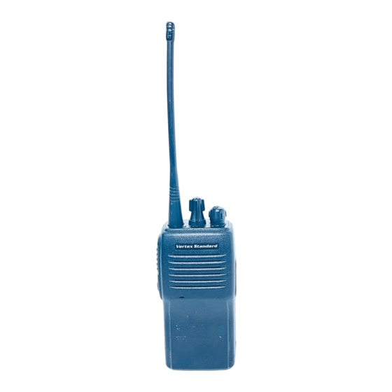
UHF FM Transceiver
VX-160EU/-180EU
Service Manual
©2004 VERTEX STANDARD CO., LTD.
Introduction
This manual provides technical information necessary for servicing the VX-160EU and VX-180EU FM Transceiver.
Servicing this equipment requires expertise in handling surface-mount chip components. Attempts by non-qualified
persons to service this equipment may result in permanent damage not covered by the warranty, and may be illegal in
some countries.
Two PCB layout diagrams are provided for each double-sided circuit board in the transceiver. Each side of is referred
to by the type of the majority of components installed on that side ("leaded" or "chip-only"). In most cases one side has
only chip components, and the other has either a mixture of both chip and leaded components (trimmers, coils, electrolytic
capacitors, ICs, etc.), or leaded components only.
While we believe the technical information in this manual to be correct, VERTEX STANDARD assumes no liability
for damage that may occur as a result of typographical or other errors that may be present. Your cooperation in pointing
out any inconsistencies in the technical information would be appreciated.
Operating Manual Reprint ............................ 2
Cloning .............................................................. 6
Specifications ................................................... 7
Exploded View & Miscellaneous Parts ...... 8
All manuals and user guides at all-guides.com
EC037U90B
VX-160EU
Contents
VERTEX STANDARD CO., LTD.
4-8-8 Nakameguro, Meguro-Ku, Tokyo 153-8644, Japan
VERTEX STANDARD
US Headquarters
10900 Walker Street, Cypress, CA 90630, U.S.A.
YAESU EUROPE B.V.
P.O. Box 75525, 1118 ZN Schiphol, The Netherlands
YAESU UK LTD.
Unit 12, Sun Valley Business Park, Winnall Close
Winchester, Hampshire, SO23 0LB, U.K.
VERTEX STANDARD HK LTD.
Unit 5, 20/F., Seaview Centre, 139-141 Hoi Bun Road,
Kwun Tong, Kowloon, Hong Kong
VX-180EU
Block Diagram ................................................. 9
Circuit Description ................................11
Alignment .................................................13
Board Unit (Schematics, Layouts & Parts)
MAIN Unit ................................................................ 17
1
Advertisement

Related Manuals for Vertex Standard VX-160EU


Summary of Contents for Vertex Standard VX-160EU
-
Page 1: Table Of Contents
ICs, etc.), or leaded components only. While we believe the technical information in this manual to be correct, VERTEX STANDARD assumes no liability for damage that may occur as a result of typographical or other errors that may be present. Your cooperation in pointing out any inconsistencies in the technical information would be appreciated. -
Page 2: Operating Manual Reprint
All manuals and user guides at all-guides.com Operating Manual Reprint Controls & Connectors Controls & Connectors Controls & Connectors Controls & Connectors Controls & Connectors Before You Begin Before You Begin Before You Begin Before You Begin Before You Begin Battery Pack Installation and Removal LED Indicator To install the battery, hold the transceiver with your... - Page 3 Hold Hold Hold None functions can be customized (set to other functions), via Monitor programming by your VERTEX STANDARD dealer, to Squelch off Low Power meet your communications/network requirements. The Lock* possible Soft key programming features are illustrated at Lamp*...
- Page 4 Tone squelch (For the 5-Tone mode, please ask ity Channel regularly as you scan the other channels. Thus, to your nearest Vertex Standard dealers). if only Channels 1, 3, and 5 (of the 8 available channels) are designated for “Scanning,” the user may nonetheless Squelch OFF assign Channel as the “User-assigned”...
- Page 5 For fur- Press (or press and hold) the assigned Soft key to send ther details contact your nearest Vertex Standard dealer. the 5-Tone sequential Code which is set to the present chan- Groupe (32 Channel Version only) nel.
-
Page 6: Cloning
All manuals and user guides at all-guides.com Cloning The VX-160E/-180E includes a convenient Cloning feature, which allows the programming data from one transceiver to be transferred to another VX-160E/-180E. Here is the procedure for Cloning one radio's data to another. 6. -
Page 7: Specifications
All manuals and user guides at all-guides.com Specifications GENERAL Specifications Frequency Range (MHz): 440 - 470 (TYP CS) 400 - 430 (TYP AS1) 420 - 450 (TYP B) 450 - 490 (TYP D) Number of Channels: 16 channels, 32 channels (32 Channel Version) Channel Spacing: 12.5 / 25 kHz PLL Steps... -
Page 8: Exploded View & Miscellaneous Parts
All manuals and user guides at all-guides.com Exploded View & Miscellaneous Parts RA0414400 (Lot. 1-12) RA041440A (Lot. 13-21) RA041440B (Lot. 22-) REF. VXSTD P/N Description Qty. FRONT CASE ASSY (VX-160E) U44104002 TAPTITE SCREW M2X4NI U44104002 TAPTITE SCREW M2X4NI (VX-180E) U20206007 BINDING HEAD SCREW M2.6X6B RA0173500 U24110002... -
Page 9: Block Diagram
All manuals and user guides at all-guides.com Block Diagram... - Page 10 All manuals and user guides at all-guides.com Block Diagram Note:...
-
Page 11: Circuit Description
All manuals and user guides at all-guides.com Circuit Description Receive Signal Path Squelch Control Incoming RF from the antenna jack is delivered to the The squelch circuitry consists of a noise amplifier and RF Unit and passes through a low-pass filter consisting of band-pass filter within Q1048 (TA31136FN), and noise coils L1001, L1002, and L1003, capacitors C1001, C1002, detector D1036 (1SS400 TE-61). - Page 12 All manuals and user guides at all-guides.com Circuit Description Automatic Transmit Power Control according to a control signal from the data latch section of Current from the final amplifier is sampled by R1020, Q1050, before being sent to the programmable divider R1039, and R1042, and is rectified by Q1003 (IMZ2A section of Q1050.
-
Page 13: Alignment
20° and 30°C (68°~ 86°F). When the transceiver is brought by the warranty policy. Also, Vertex Standard must re- into the shop from hot or cold air, it should be allowed serve the right to change circuits and alignment proce- time to come to room temperature before alignment. - Page 14 All manuals and user guides at all-guides.com Alignment Set up the test equipment as shown below for transceiver alignment, and apply 7.5V DC power to the transceiver. Tone-Frequency (Hz) / DCS-code Channel CTCSS Low Band Edge – – (Channel 1) Band Center 67.0 Signal Generator...
- Page 15 All manuals and user guides at all-guides.com Alignment PLL Reference Frequency PLL VCV (Varactor Control Voltage) Set the transceiver to CH 2 via the “CH” box located Connect the DC voltmeter between TP1025 on the on the upper left corner on the “Alignment” window Main Unit and ground.
- Page 16 All manuals and user guides at all-guides.com Alignment Low Power CTCSS Deviation Set the transceiver to CH 1 via the “CH” box located Set the transceiver to CH 3 via the “CH” box located on the upper left corner on the “Alignment” window on the upper left corner on the “Alignment”...
-
Page 17: Main Unit
All manuals and user guides at all-guides.com MAIN Unit (Lot. 1~4) Q1048 1 [4.93V] 6 [4.6V] 11 [4.08V] 2 [4.58V] 7 [1.51V] 12 [0.44V] Circuit Diagram 3 [3.74V] 8 [0.66V] 14 [1.75V] 4 [4.96V] 9 [1.08V]{1.26} 15 [0V] 5 [4.6V] 10 [4.96V] 16 [0.96V] [5.01V]... - Page 18 All manuals and user guides at all-guides.com MAIN Unit (Lot. 1~4) Note:...
- Page 19 All manuals and user guides at all-guides.com MAIN Unit (Lot. 1~4) Parts Layout Side A LC75834W NJM12903R RT1N441U (N3) 2SC4154E (LE) DTC124TE (05) FMW1 (W1) MC2850 (A7) FA1101F (Q1033) (Q1045) (Q1052) (Q1022, 1028, (Q1032) (Q1002) (D1033) (D1021, 1022) 1046, 1053) NJM2902V NJM2070M 2SA1602A (MF)
- Page 20 All manuals and user guides at all-guides.com MAIN Unit (Lot. 1~4) Parts Layout Side B M37516F8HP S-29430AFE MB15A02PFV1 2SC4154E (LE) 2SA1602A (MF) 2SK2973 (K1) 2SK2974 2SK508 (K52) DTA114EU (14) RT1N441U (N3) CPH6102 (AB) NJM2871AF05 (82) DAN235E (M) (Q1011) (Q1008) (Q1050) (Q1005, 1026, (Q1031, 1051) (Q1009)
- Page 21 All manuals and user guides at all-guides.com MAIN Unit (Lot. 5~) Circuit Diagram...
- Page 22 All manuals and user guides at all-guides.com MAIN Unit (Lot. 5~) Note:...
- Page 23 All manuals and user guides at all-guides.com MAIN Unit (Lot. 5~) Parts Layout Side A LC75834W NJM12903R RT1N441U (N3) 2SC4154E (LE) DTC124TE (05) FMW1 (W1) MC2850 (A7) FA1101F (Q1033) (Q1045) (Q1052) (Q1022, 1028, (Q1032) (Q1002) (D1033) (D1021, 1022) 1046, 1053) NJM2902V NJM2070M 2SA1602A (MF)
- Page 24 All manuals and user guides at all-guides.com MAIN Unit (Lot. 5~) Parts Layout Side B M37516F8HP S-29430AFE (16 CH) MB15A02PFV1 2SC4154E (LE) 2SA1602A (MF) 2SK2973 (K1)(Lot. 1~19) 2SK2974 (Lot. 1~19) 2SK508 (K52) DTA114EU (14) RT1N441U (N3) CPH6102 (AB) NJM2871AF05 (82) DAN235E (M) (Q1011) S-29530ADFJA (32 CH)
- Page 25 All manuals and user guides at all-guides.com MAIN Unit Parts List REF. DESCRIPTION VALUE TOL. MFR’S DESIG VXSTD P/N VERS. LOT. SIDE LAY ADR PCB with Components CB2038001 VX-160E VERSION CS1, CH16 CB2038002 VX-180E VERSION CS1, CH16 CB2038003 VX-160E VERSION AS1, CH16 CB2038004 VX-180E VERSION AS1, CH16 CB2038005 VX-180E VERSION CS1, CH32 Printed Circuit Board...
- Page 26 All manuals and user guides at all-guides.com MAIN Unit REF. DESCRIPTION VALUE TOL. MFR’S DESIG VXSTD P/N VERS. LOT. SIDE LAY ADR C 1045 CHIP CAP. 100pF UMK105CH101JW-F K22178282 C 1046 CHIP TA.CAP. 10uF TEMSVB21C106M-8R K78120025 C 1047 CHIP CAP. 0.001uF UMK105B102KW-F K22178829...
- Page 27 All manuals and user guides at all-guides.com MAIN Unit REF. DESCRIPTION VALUE TOL. MFR’S DESIG VXSTD P/N VERS. LOT. SIDE LAY ADR C 1095 CHIP CAP. 0.001uF UMK105B102KW-F K22178829 C 1096 CHIP CAP. UMK105CH040CW-F K22178252 C 1097 CHIP CAP. UMK105CK020CW-F K22178250 C 1098 CHIP CAP.
- Page 28 All manuals and user guides at all-guides.com MAIN Unit REF. DESCRIPTION VALUE TOL. MFR’S DESIG VXSTD P/N VERS. LOT. SIDE LAY ADR C 1138 CHIP CAP. 680pF UMK105B681KW-F K22178827 VX-180 C 1139 CHIP CAP. 0.1uF LMK105BJ104KV-F K22108806 VX-180 C 1140 CHIP TA.CAP. TESVA1C105M1-8R K78120009 VX-180 C 1141 CHIP CAP.
- Page 29 All manuals and user guides at all-guides.com MAIN Unit REF. DESCRIPTION VALUE TOL. MFR’S DESIG VXSTD P/N VERS. LOT. SIDE LAY ADR C 1202 CHIP CAP. 0.022uF EMK105B223KW-F K22128813 C 1203 CHIP CAP. 0.1uF LMK105BJ104KV-F K22108806 C 1204 CHIP CAP. 0.01uF GRM36B103K16PT K22128804...
- Page 30 All manuals and user guides at all-guides.com MAIN Unit REF. DESCRIPTION VALUE TOL. MFR’S DESIG VXSTD P/N VERS. LOT. SIDE LAY ADR C 1273 CHIP CAP. 100pF UMK105CH101JW-F K22178282 C 1274 CHIP CAP. 100pF UMK105CH101JW-F K22178282 C 1275 CHIP CAP. 0.001uF UMK105B102KW-F K22178829...
- Page 31 Q 1010 TRANSISTOR RT1P441U-T11-1 G3070248 Q 1011 IC M37516F8HP 1-41 Q 1011 IC M37516F8HP R0841 16 CHANNELS 42- Q 1011 IC M37516F8HP R0842 32 CHANNELS 42- Q 1012 TRANSISTOR RT1N441U-T11-1 G3070247 Q 1013 TRANSISTOR 2SC5006-T1 G3350068 Please contact VERTEX STANDARD.
- Page 32 All manuals and user guides at all-guides.com MAIN Unit REF. DESCRIPTION VALUE TOL. MFR’S DESIG VXSTD P/N VERS. LOT. SIDE LAY ADR Q 1014 TRANSISTOR 2SC3357-T2 RF G3333577F Q 1015 TRANSISTOR RT1P441U-T11-1 G3070248 Q 1016 TRANSISTOR CPH6102-TL G3070223 Q 1017 IC NJM2902V-TE1 G1091679 Q 1018 TRANSISTOR...
- Page 33 All manuals and user guides at all-guides.com MAIN Unit REF. DESCRIPTION VALUE TOL. MFR’S DESIG VXSTD P/N VERS. LOT. SIDE LAY ADR R 1027 CHIP RES. 2.2k 1/16W 5% RMC1/16S 222JTH J24189029 R 1029 CHIP RES. 1.5k 1/16W 5% RMC1/16S 152JTH J24189027 R 1030 CHIP RES.
- Page 34 All manuals and user guides at all-guides.com MAIN Unit REF. DESCRIPTION VALUE TOL. MFR’S DESIG VXSTD P/N VERS. LOT. SIDE LAY ADR R 1090 CHIP RES. 1/16W 5% RMC1/16S 270JTH J24189006 VERSION D R 1091 CHIP RES. 1/16W 5% RMC1/16S 103JTH J24189037 R 1092 CHIP RES.
- Page 35 All manuals and user guides at all-guides.com MAIN Unit REF. DESCRIPTION VALUE TOL. MFR’S DESIG VXSTD P/N VERS. LOT. SIDE LAY ADR R 1157 CHIP RES. 1/16W 5% RMC1/16S 220JTH J24189005 R 1158 CHIP RES. 1/16W 5% RMC1/16S 391JTH J24189020 R 1159 CHIP RES.
- Page 36 All manuals and user guides at all-guides.com MAIN Unit REF. DESCRIPTION VALUE TOL. MFR’S DESIG VXSTD P/N VERS. LOT. SIDE LAY ADR R 1225 CHIP RES. 1/16W 5% RMC1/16S 123JTH J24189038 R 1226 CHIP RES. 1/16W 5% RMC1/16S 123JTH J24189038 R 1227 CHIP RES.
- Page 37 All manuals and user guides at all-guides.com Copyright 2004 VERTEX STANDARD CO., LTD. All rights reserved No portion of this manual may be reproduced without the permission of VERTEX STANDARD CO., LTD.
Need help?
Do you have a question about the VX-160EU and is the answer not in the manual?
Questions and answers