HIKVISION DS7208HVI-ST Product/Maintenance Manual
Hide thumbs
Also See for DS7208HVI-ST:
- Technical manual (9 pages) ,
- User manual (101 pages) ,
- Quick operation manual (40 pages)
Table of Contents
Advertisement
Quick Links
Product Maintenance Manual
Functional Characteristics:
VGA video output resolution topped 1024 * 768;
Partial digital zoom by using mouse when in HIKVISION PTZ control mode
The first channel support 4CIF/2CIF/CIF/QCIF real-time coding, the others
channel support CIF/QCIF real-time coding;
Support preview images and playback image of electronic amplification;
VGA, VIDEO OUT can be simultaneously screen preview, of which the main
output can output menu operation;
Support four channel synchronous playback;
Support one SATA interface;
Support NTP (network school), SADP (automatic search IP address)
agreement.
(HIK/DS7208HVI-ST/SN)
Advertisement
Table of Contents

Related Manuals for HIKVISION DS7208HVI-ST


Summary of Contents for HIKVISION DS7208HVI-ST
-
Page 1: Functional Characteristics
(HIK/DS7208HVI-ST/SN) Functional Characteristics: VGA video output resolution topped 1024 * 768; Partial digital zoom by using mouse when in HIKVISION PTZ control mode The first channel support 4CIF/2CIF/CIF/QCIF real-time coding, the others channel support CIF/QCIF real-time coding;... -
Page 2: Table Of Contents
1. DS7208HVI-ST/SN Equipment Physical Interface 2. DS7208HVI-ST/SN Equipment Internal Structure 3. DS80061 Mainboard Hardware Principle Diagram 4. DS80061 Mainboard Hardware Modules Diagram 5. DS80061 Mainboard Hardware Module Introduction 5.1. Audio Video A/D Module 5.2. VGA Output Module (Local Preview Image Output Module) 5.3 VOUT Output Module (Local Preview Image Output Module) -
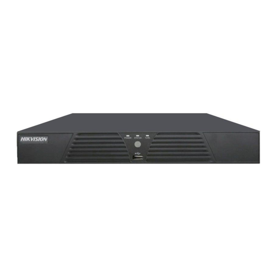
Page 3: Ds7208Hvi-St/Sn Equipment Physical Interface
1. DS7208HVI-ST/SN Equipment Physical Interface Note: Note: The back panel is similar to7208HVI-ST/SN(7216HVI-ST/SN) 2. DS7208HVI-ST/SN Equipment Internal Structure 12V power interfac SATA power interface SATA interface USB interface Panel line interface Panel line USB line Front-panel Note: the front panel no menu operation function... -
Page 4: Ds80061 Mainboard Hardware Principle Diagram
3. DS80061 Mainboard Hardware Principle Diagram DDR∏ FLASH Network interface (RTL8201) Video in TW2866 Audio in LVC07A+6303 (US1) Audio out AOUT SGM9111 VOUT 6LB18 RS232 SATA RS485 Diagram1.1 DS80061 Hardware Principle Diagram Note: TW2866 (US1) support 1 road audio and 4 road video input, voice talkback Line In input ... -
Page 5: Ds80061 Mainboard Hardware Modules Diagram
4. DS80061 Mainboard Hardware Modules Diagram VGAmodule VOUT module Network module Power module Network module A/D module SATA Clock module power module USB interface RS232 interface SATA interface Front-panel interface RS485module Diagram 1.2 DS80061 Mainboard Hardware Modules Diagram... -
Page 6: Ds80061 Mainboard Hardware Module Introduction
5. DS80061 Mainboard Hardware Module Introduction 5.1. Audio Video A/D Module Video A/D Module Main Control Chip:TW2866 Audio TW2866(US1)PIN 6 control first audio input(input matching resistance 100 (RU9) and capacitance (CS18)) TW2866(US1)PIN 13/17/21/25 control 1-4 road vedio input(BNC input ... -
Page 7: Vga Output Module (Local Preview Image Output Module)
5.2. VGA Output Module (Local Preview Image Output Module) VGA main chip module: LVC07A, 6303; LVC07A PIN 2 output single(VS) and 1 K resistance (RL50) connect 5V voltage, PIN 4 output signal (HS) and 1 K (RL51) resistance connect 5V voltage BAV99: control VGA output amplification, if BAV99 (Q9) 3 feet low level ... -
Page 8: Vout Output Module (Local Preview Image Output Module)
RL50 Ω VS(Interlacing signal) PIN4 74LV07 HS(Line signal) PIN2 RL51 Ω BAV99 : If the PIN 3 of BAV99(Q9) is Low-level ( 0V ), Said system detects VGA monitor; If the PIN 3 of BAV99(Q9) is high-level (nearly 3.3V),said system doesn’t detect VGA monitor;... -
Page 9: Network Module
WCX(FBS48) for 5V power supply VOUT interface TVS protection tube: VOUT interface connect HK-5 (TVS9) VOUT signal output basic schemes: FBS48 Pin5 CVBS-VOUT Pin4 output Pin3 input SGM9111 VOUT 75Ω(RS117) 75Ω (RS188) VOUT Module components: 75Ω(RS117) HK-5 (TVS9) WCX (FBS48)... -
Page 10: Sata Module
MS10232 RTL8201 BV03C (TVS32/17) 25M (Y3) WCX (FBN1) 5.4.1 LAN master chip : Chip name Description voltage Operation voltage RTL8201 input “pin 36” via V≈3.3V “FBN1” 5.4.2 Transformer Chip name Description Network transmission signal MS10232NL amplification, rectification 5.4.3 Crystal Chip name Description 25M(Y3) RTL8201 clock chip... -
Page 11: Rs485 Module
BD9329 (U1) SATA power interface SATA interface 5.6. RS485 Module RS485 main control chip:6LB184, PIN 6, 7 were TX +,TX-,the difference voltage close to 5 V TVS(B03NC):B03NC(BA2、BA7)protect the sending end (TX +, TX-R +, Thermistors (JK250) : JK250 (RPT1/2) protect the sending end (TX +, TX-R ... -
Page 12: Clock Module
5.7. Clock Module Clock control chip: 8563 T 32768 HZ: 8563 T reset the clock Battery: External Battery, normal voltage 3.3 V Diodes (DG1, DG2, DG3) : DG1 connects to 3.3 V voltage, DG2, DG3 Battery are connected at one end, when the mainboard electricity, DG2, DG3 globe, DG1 conduction, Battery don't power supply;... -
Page 13: Power Supply Module
TW2866 (US1) 3.9K(RS60) 390Ω(RP24) (note: voice talkback Line In input and the first road audio input share) 5.9. Power Supply Module The power module component: BD9329(U1) BD9328(U3) BD9328(U5) BD00IC0WE BD9329 (U1) : 2 feet enter 12 V, 3 feet output 5 V, mainly for the SATA hard disk normal ... -
Page 14: Ds80061 Mainboard Failure Analysis
6. DS80061 Mainboard Failure Analysis VGA and VOUT and output image, but not at the same time output system menu, the system default first detection VGA output, then detection VOUT output 6.1. First Meet VGA Display Boot to meet VGA monitor (or also meet VGA display and VOUT monitor), BAV99 (Q6) PIN 3 low level effective, display output VGA signal and system menu, monitor only VOUT signal 6.2. - Page 15 ②. No VOUT Output Step 1: measurement HK-5 (TVS9) whether short circuit, or replacement Step 2: measuring 75Ωresistance (RS117) impedence, or replacement Step 3: monitor’s signal lines connected to the probe, directly from SGM9111 (US7) chip PIN 4 draw out the VOUT signal, or replacement Step 4: measuring 75Ω...
- Page 16 ⑤.RS485 Failure Step 1: the first to exclude thermistors JK250 (RPT1/2) Step 2: measurement TVS tube B03NC (BA2/7) impedance, or replacement Step 3: measurement 6L184 6and 7 feet chip difference voltage (normal close to 5 V), or replacement ⑥. Internet Links Network light and network data transmission light are flashing ...
- Page 17 ⑩.USB Fault Step one: measurement SESR05 (QA1 or QA2) 2, 3 feet voltage difference value (normal voltage difference about 3.05 V), as well as the impedance to the GND, or replacement Note: SESR05 (QA1 or QA2),front and after USB interface is independent of each other SESR05 (...
-
Page 18: Schedule: 1 Crystal Effect
Schedule: 1 Crystal Effect Serial Crystals Action (devices work clock) number 27M(Y4) TW2866 chips work clock (82 feet input 27 M) 25M(Y3) RTL8201 chips work clock 24M(Y1) KY2010 system startup clock, and integrated USB module clock Schedule:2 Voltage Effect The serial Power chip function (devices working voltage) number...
Need help?
Do you have a question about the DS7208HVI-ST and is the answer not in the manual?
Questions and answers