Icom IC-F40GT Service Manual
Including mt version
Hide thumbs
Also See for IC-F40GT:
- Instruction manual (44 pages) ,
- Service manual (7 pages) ,
- Servise manual (42 pages)
Table of Contents
Advertisement
Quick Links
Advertisement
Table of Contents

Related Manuals for Icom IC-F40GT


Summary of Contents for Icom IC-F40GT
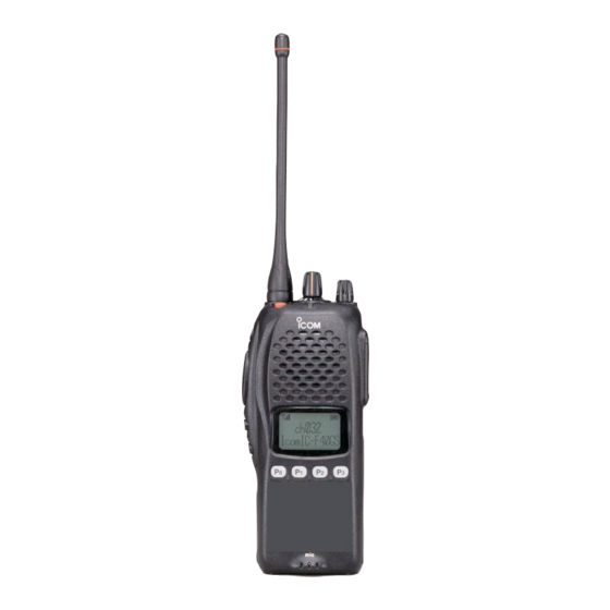
- Page 1 UHF TRANSCEIVER iC-f40gt iC-f40gs iC-f4 1 gt iC-f4 1 gs ( including MT version )
- Page 2 This could damage the transceiver’s front end. INTRINSICALLY SAFE QUALIFICATION When servicing intrinsically safe versions of the IC-F40GT/GS and IC-F41GT/GS the following conditions must be met. Failing to satisfy any of these conditions will invalidate the INTRINSICALLY SAFE certification.
-
Page 3: Table Of Contents
EXPLICIT DEFINITIONS FREQUENCY COVERAGE CHANNEL SPACING Wide/Narrow-type 25 kHz/12.5 kHz L-band 400–430 MHz ML-band 440–480 MHz Middle/Narrow-type 20 kHz/12.5 kHz M-band MH-band 450–490 MHz H1-band 480–512 MHz H-band H2-band 480–520 MHz TABLE OF CONTENTS SECTION 1 SPECIFICATIONS SECTION 2 INSIDE VIEWS SECTION 3 DISASSEMBLY INSTRUCTIONS SECTION 4... - Page 4 SECTION 1 SPECIFICATIONS USA/GEN Measurement method EIA-152-C/204D or TIA-603 ETS 300 086 (GEN) [L-band]: 400.000–430.000 MHz [ML-band]: 440.000–480.000 MHz [GEN]/[EUR] Frequency coverage [MH-band]: 450.000–490.000 MHz [USA]/[GEN] [H-band]: 480.000–512.000 MHz [USA], 480.000–520.000 MHz [GEN] 16K0F3E [25 kHz; Wide], 8K50F3E [12.5 kHz; Narrow] Type of emission 14K0F3E [20 kHz;...
-
Page 5: Inside Views
SECTION 2 INSIDE VIEWS • MAIN UNIT Top view Antenna switching D/A converter (D25, D24: MA77) (IC27: M62334) (D1: 1SV307) • FRONT UNIT Power detector (D2, D3: RB706F) APC amplifier Bottom view Power amplifier (IC4: TC75S51F) (Q1: 2SK2974) 2nd IF filter (450 kHz Internal speaker switch circuit Pre-drive amplifier (FI2: SFPCA450KE4A) - Page 6 (2 × w Unscrew 1 screw w Unscrew 2 nuts (ICOM screw), and 2 screws (2 × 4 mm, silver), and 2 screws e Unscrew 6 screws 4 mm, black) from the 9-pin connector. (2 × 8 mm, silver) from the chassis.
-
Page 7: Circuit Description
SECTION 4 CIRCUIT DESCRIPTION 4-1 RECEIVER CIRCUITS The RF signals from the bandpass filter are mixed with the 1st LO signals, where come from the RX VCO circuit via the 4-1-1 ANTENNA SWITCHING CIRCUIT attenuator (R108–R106), at the 1st mixer circuit (Q19) to The antenna switching circuit functions as a low-pass filter produce a 47.25 MHz 1st IF signal. -
Page 8: Transmitter Circuits
4-1-5 AF AMPLIFIER CIRCUIT 4-2 TRANSMITTER CIRCUITS The AF amplifier circuit amplifies the demodulated AF sig- 4-2-1 MICROPHONE AMPLIFIER CIRCUIT nals to drive a speaker. The microphone amplifier circuit amplifies audio signals within +6 dB/octave pre-emphasis characteristics from the The AF signals from the FM IF IC (IC3, pin 9) are amplified microphone to a level needed for the modulation circuit. -
Page 9: Pll Circuit
4-2-4 APC CIRCUIT 4-3 PLL CIRCUITS The APC circuit (IC4, Q22) protects the YGR (IC-F41GT/GS 4-3-1 PLL CIRCUIT only), drive and power amplifiers from excessive current A PLL circuit provides stable oscillation of the transmit fre- drive, and selects output power of HIGH, LOW2 or LOW1. quency and receive 1st LO frequency. - Page 10 4-4 FFSK CIRCUIT DESCRIPTION In case of the FFSK signal is used for the PM modulation, the FM/PM switch (IC26) is changed to pin 6. 4-5-1 GENERAL IC9 is the compounder IC which is controlled by serial data In case of the FFSK signal is used for the FM modulation, bus line (“TRD”, “MSKE”, “DIN”, “SCK”, “APST”, “REGS1”, the FM/PM switch (IC26) is changed to pin 7.
-
Page 11: Power Supply Circuits
4-5 POWER SUPPLY CIRCUIT PORT DESCRIPTION NAME VOLTAGE LINE Outputs data signals for the PLL IC LINE DESCRIPTION (IC1), compamder IC (IC9), expander The voltage from the attached battery pack. IC (IC23), D/A converter (IC13), etc. Outputs strobe signals to the D/A con- The same voltage as the HV line (battery volt- DAST verter (IC13). -
Page 12: Adjustment Procedures
Connect to GND Battery type detector Battery type detector I STARTING SOFTWARE ADJUSTMENT q Connect IC-F40GT, F40GS, F41GT or F41GS and PC with *OPC-966 JIG CABLE w Turn the transceiver power ON. e Boot up Windows, and click the program group ‘CS-F30G ADJ’... - Page 13 • Screen display exampe (for conventional version) CS-F30G ADJ Rev.1.0 File Option COM 1: OPEN Connect Reload (F5) Disp para [A / D] [D / A] : 197 : C5h : 7.73 V BPF T1 : 90 : 5Ah : 1.76 V TEMPS : 190 : BEh : 32.23 'C BPF T2...
- Page 14 Connect to GND folder of the [Start] menu. Battery type detector Battery type detector I STARTING SOFTWARE ADJUSTMENT q Connect IC-F40GT, F40GS, F41GT or F41GS and PC with *OPC-966 JIG CABLE w When “MAP27” setting is [Disable], turn the transceiver power ON.
- Page 15 • Screen display exampe (for MPT version) CS-F40G ADJ Rev.1.0 File Option COM 1: OPEN Connect Reload (F5) Disp para [A / D] [D / A] : 197 : C5h : 7.73 V BPF T1 : 90 : 5Ah : 1.76 V TEMPS : 190 : BEh : 32.23 'C BPF T2...
- Page 16 • Connection (common) Standard signal generator to the antenna connector 0.1 µV to 32 mV (–127 dBm to –17 dBm) Attenuator deviation meter 40 dB or 50 dB CAUTION: DO NOT transmit while RF power meter 0.1–10 W/50 Ω SSG is connected to the antenna connector.
-
Page 17: Pll Adjustment
5-2 PLL ADJUSTMENT MEASUREMENT ADJUSTMENT ADJUSTMENT ADJUSTMENT CONDITIONS VALUE UNIT LOCATION UNIT ADJUST PLL LOCK • Operating freq. : 400.000 MHz MAIN Connect a digital multi- 1.3 V MAIN C372 VOLTAGE 440.000 MHz [ML] meter or an oscillo- 450.000 MHz [MH] scope to the check 480.000 MHz point, “CP7”. -
Page 18: Software Adjustment
5-3 SOFTWARE ADJUSTMENT Select an operation using [↑] / [↓] keys, then set specified value using [←] / [→] keys on the connected computer keyboard. MEASUREMENT ADJUSTMENT ADJUSTMENT CONDITION VALUE UNIT LOCATION REFERENCE • Operating freq. : 430.000 MHz Loosely couple a frequnecy 430.0000 MHz [L] FREQUENCY 480.000 MHz... - Page 19 SOFTWARE ADJUSTMENT – continued Select an operation using [↑] / [↓] keys, then set specified value using [←] / [→] keys on the connected computer keyboard. MEASUREMENT ADJUSTMENT ADJUSTMENT CONDITION VALUE UNIT LOCATION ±0.70 kHz [Wide] A CTCSS/DTCS • Operating freq. : 400.000 MHz Connect an FM deviation meter DEVIATON 440.000 MHz...
- Page 20 SOFTWARE ADJUSTMENT – continued Select an operation using [↑] / [↓] keys, then set specified value using [←] / [→] keys on the connected computer keyboard. “S-METER (or RSSI L0/L2—[MPT])” adjustment must be performued after “RX SENSITIVITY” adjustment (at page 5-8) is finished. MEASUREMENT ADJUSTMENT ADJUSTMENT CONDITION...
-
Page 21: Parts List
M.=Mounted side (T: Mounted on the Top side, B: Mounted on the Bottom side) [L]: L-band, [ML]: ML-band, [MH]: MH-band, [H]: H-band, [M]: ML and MH bands, *=Safety critical components [GT]: IC-F40GT/F41GT, [GS]: IC-F40GS/F41GS, [F40G]: IC-F40GT/F40GS, S.=Surface mount [F41G]: IC-F41GT/F41GS, [IS]: Intrinsically safe version, [BIIS]: BIIS version... - Page 22 M.=Mounted side (T: Mounted on the Top side, B: Mounted on the Bottom side) [L]: L-band, [ML]: ML-band, [MH]: MH-band, [H]: H-band, [M]: ML and MH bands, *=Safety critical components [GT]: IC-F40GT/F41GT, [GS]: IC-F40GS/F41GS, [F40G]: IC-F40GT/F40GS, S.=Surface mount [F41G]: IC-F41GT/F41GS, [IS]: Intrinsically safe version, [BIIS]: BIIS version...
- Page 23 M.=Mounted side (T: Mounted on the Top side, B: Mounted on the Bottom side) [L]: L-band, [ML]: ML-band, [MH]: MH-band, [H]: H-band, [M]: ML and MH bands, *=Safety critical components [GT]: IC-F40GT/F41GT, [GS]: IC-F40GS/F41GS, [F40G]: IC-F40GT/F40GS, S.=Surface mount [F41G]: IC-F41GT/F41GS, [IS]: Intrinsically safe version, [BIIS]: BIIS version...
- Page 24 M.=Mounted side (T: Mounted on the Top side, B: Mounted on the Bottom side) [L]: L-band, [ML]: ML-band, [MH]: MH-band, [H]: H-band, [M]: ML and MH bands, *=Safety critical components [GT]: IC-F40GT/F41GT, [GS]: IC-F40GS/F41GS, [F40G]: IC-F40GT/F40GS, S.=Surface mount [F41G]: IC-F41GT/F41GS, [IS]: Intrinsically safe version, [BIIS]: BIIS version...
- Page 25 M.=Mounted side (T: Mounted on the Top side, B: Mounted on the Bottom side) [L]: L-band, [ML]: ML-band, [MH]: MH-band, [H]: H-band, [M]: ML and MH bands, *=Safety critical components [GT]: IC-F40GT/F41GT, [GS]: IC-F40GS/F41GS, [F40G]: IC-F40GT/F40GS, S.=Surface mount [F41G]: IC-F41GT/F41GS, [IS]: Intrinsically safe version, [BIIS]: BIIS version...
- Page 26 [L]: L-band, [ML]: ML-band, [MH]: MH-band, [H]: H-band, [M]: ML and MH bands, M.=Mounted side (T: Mounted on the Top side, B: Mounted on the Bottom side) [GT]: IC-F40GT/F41GT, [GS]: IC-F40GS/F41GS, [F40G]: IC-F40GT/F40GS, *=Safety critical components [F41G]: IC-F41GT/F41GS, [IS]: Intrinsically safe version, [BIIS]: BIIS version S.=Surface mount...
- Page 27 [L]: L-band, [ML]: ML-band, [MH]: MH-band, [H]: H-band, [M]: ML and MH bands, M.=Mounted side (T: Mounted on the Top side, B: Mounted on the Bottom side) [GT]: IC-F40GT/F41GT, [GS]: IC-F40GS/F41GS, [F40G]: IC-F40GT/F40GS, *=Safety critical components [F41G]: IC-F41GT/F41GS, [IS]: Intrinsically safe version, [BIIS]: BIIS version S.=Surface mount...
- Page 28 [F41G], [BIIS] only [L]: L-band, [ML]: ML-band, [MH]: MH-band, [H]: H-band, [M]: ML and MH bands, [GT]: IC-F40GT/F41GT, [GS]: IC-F40GS/F41GS, [F40G]: IC-F40GT/F40GS, [F41G]: IC-F41GT/F41GS, [IS]: Intrinsically safe version, [BIIS]: BIIS version M.=Mounted side (T: Mounted on the Top side, B: Mounted on the Bottom side) *=Safety critical components S.=Surface mount...
- Page 29 8210017091 2337 terminal holder-1 [GT] : IC-F40GT/F41GT MP44 8950005311 Antenna connector-103-1 [GS] : IC-F40GS/F41GS MP49 8510013220 2337 antenna plate [F40G] : IC-F40GT/F40GS MP50 8930053440 2337 A-PTT plate [F41G] : IC-F41GT/F41GS MP51 8930053431 Sponge (GP)-1 MP52 8820000801 1327 screw-1 MP53 8930053630...
- Page 30 MP40 (C) W1 (F) MP2 (F) MP40 (C) MP5 (C) MP51 (C) MP19 (C) MP65 (C) MP20 (C) SP1 (F) MP26 (C) MP17 (C) MP57 (C) N I T MP54 (C) MP10 (C) MP40 (C) MP8 (C) MP55 (C) MP3 (F) MP44 (C) MP50 (C) MP53 (C)
- Page 31 SECTION SECTION 8 PARTS LIST SEMI-CONDUCTOR INFORMATION 8 - 1 TRANSISTORS AND FETS 8 - 2 DIODES NAME SYMBOL INSIDE VIEW NAME SYMBOL INSIDE VIEW NAME SYMBOL INSIDE VIEW NAME SYMBOL INSIDE VIEW 3SK206-T1 U78 1SS355 2SA1362 GR MA77 3SK293 1SV307 CPH3403-TL 1SS375...
- Page 32 SECTION 9 BOARD LAYOUTS 9 - 1 FRONT UNIT • TOP VIEW The combination of this page and the next page shows the unit layout in the same configuration as the actual MICROPHONE P.C. Board. ✽ 9 - 1...
- Page 33 FRONT unit The combination of this page and the previous page • BOTTOM VIEW shows the unit layout in the same configuration as the actual P.C. Board. VOUT VEE3 VEE2 CAP+ CAP– PMODE OSC1 OSC0 RESB VS/TE SPEAKER to MAIN unit J3 9 - 2...
- Page 34 9 - 2 F40G MAIN UNIT • TOP VIEW OPC-966 The combination of this page and the next page shows EM-80 the unit layout in the same configuration as the actual AD-52 HS-93 P.C. Board. UNIVERSAL CONNECTOR to FRONT unit J1 INT SP SW AF VR POWER SW...
-
Page 35: F40G Main Unit
The combination of this page and the previous page shows the unit layout in the same configuration as the F40G (MAIN unit) actual P.C. Board. • BOTTOM VIEW INT SP SW AF VR POWER SW R193 4 5 6 SELECT MP67 (CHASSIS)... - Page 36 9 - 3 F41G MAIN UNIT • TOP VIEW OPC-966 The combination of this page and the next page shows EM-80 AD-52 the unit layout in the same configuration as the actual HS-93 P.C. Board. UNIVERSAL CONNECTOR to FRONT unit J1 INT SP SW AF VR POWER SW...
-
Page 37: F41G Main Unit
The combination of this page and the previous page shows the unit layout in the same configuration as the F41G (MAIN unit) actual P.C. Board. • BOTTOM VIEW INT SP SW AF VR POWER SW R193 4 5 6 SELECT 9 - 6... -
Page 38: Disassembly Information
SECTION 10 BC-137 OPTIONAL DESKTOP CHARGER INFORMASION 10-1 PARTS LIST 10-2 DISASSEMBLY INFORMATION [MAIN UNIT] REF. NO. ODER NO. DESCRIPTION QTY. 1520000650 S.TRANSISTOR 2SB1201-S-TL MP3 (C) 1590000480 S.TRANSISTOR RN2402 (TE85R) 1590000510 S.TRANSISTOR RN1409 (TE85R) 1530001950 S.TRANSISTOR 2SC2712-GR (TE85R) 1750000550 S.DIODE 1SS355 TE-17 1750000020 S.DIODE 1SS184 (TE85R) -
Page 39: Voltage Diagram
10-3 VOLTAGE DIAGRAM 12.49 V 12.47 V 13.80 V R1 24 R5 10 k 8.01 V 7.98 V 7.20 V D2 1SS184 2SB1201 S R2 24 CHARGE+ 11.82 V 11.80 V 13.63 V 12.46 V RN2404 TEMP DS1 TLG124A R4 10 k 0.23 V 1SS355 0.22 V... - Page 40 SECTION 11 BLOCK DIAGRAM Q9: DTC144EU 2SC4116 Q10: XP1214 MAIN UNIT TA75S01F RIPPLE VCOS FILTER BIAS 1.25V 2SK880 400-520 MHz BUFF LVIN 2SC4226 D2,D3 1SV307 D4, D5: MA77 TC75S51F D24, D25: MA77 CR-667 SA7025 2SC5107 2SC5107 2SC5107 2SC3585 2SK2973 2SK2974 RB706F-40 RX VCO DRIVE...
- Page 41 C448 DETECT C355 C353 DTMF DECODE 820p 0.047 0.001 0.001 R277 1k R325 MICE XOUT R278 1k RESET Note [GT]: IC-F40GT/F41GT VIN2 R279 1k R368 XRXD XRXD R369 390k XTXD 180k XTXD [GS]: IC-F40GS/F41GS R362 C449 R280 1k R312 6.8k [H]...
- Page 42 Note [GT]: IC-F40GT/F41GT [F40G]: IC-F40GT/F40GS : L-band 400–430 MHz [H] : H-band 480–512/480–520 MHz Explanatory notes [GS]: IC-F40GS/F41GS [F41G]: IC-F41GT/F41GS [ML] : ML-band 440–480 MHz [M] : ML and MH bands C459 +B LINE TX LINE 47p [F41G] HSU88 2.2k [M] 1.8µH...
- Page 43 Unit 9, Sea St., Herne Bay, Kent, CT6 8LD, U.K. Phone : +44 (01227) 741741 Fax : +44 (01227) 741742 : http://www.icomuk.co.uk Icom (Australia) Pty. Ltd. E-mail : info@icomuk.co.uk A.B.N. 88 006 092 575 290-294 Albert Street, Brunswick, Victoria, 3056, Australia Icom France S.a...
- Page 44 S-13803MZ-C1-2 1-1-32, Kamiminami, Hirano-ku, Osaka 547-0003, Japan C 2001-2003 Icom Inc.
Need help?
Do you have a question about the IC-F40GT and is the answer not in the manual?
Questions and answers