Table of Contents
Advertisement
Quick Links
iPod is a registered trademark of Apple Inc.
[1]
Important Service Safety Precaution...... . ....... 1-1
[2]
Important Service Notes (For U.s.a Only) . ....... 1-1
[3]
Specifications ......................................... . ....... 1-2
[4]
Name Of Parts ....................................... . ....... 1-3
[1]
Mechanism Section................................ . ....... 2-1
[2]
Test Mode............................................... . ....... 2-2
[3]
Cd Section ............................................. . ....... 2-4
CHAPTER 3. MECHANISM BLOCKS
[1]
Caution On Disassembly........................ . ....... 3-1
[2]
Removing And Reinstalling The Main Parts ..... 3-4
[1]
Main Block Diagrams ............................. . ....... 4-1
[2]
Cd Block Diagrams....................................... 4-3
Parts marked with "
" are important for maintaining the safety of the set. Be sure to replace these parts with
!
specified ones for maintaining the safety and performance of the set.
SHARP CORPORATION
SERVICE MANUAL
MINI COMPONENT SYSTEM
MODEL
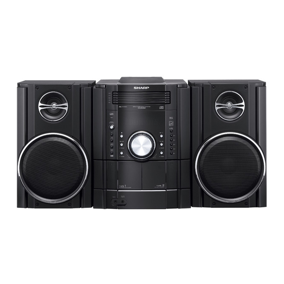
CD-DK890N Mini Component System consisting of
CD-DK890N (main unit), CP-DK890N (speaker system).
• In the interests of user-safety the set should be restored
to its original condition and only parts identical to those
specified be used.
CONTENTS
CHAPTER 5. CIRCUIT DESCRIPTION
[1]
Waveforms Of Cd Circuit ..............................5-1
[2]
Voltage...........................................................5-2
LAYOUT
[1]
Notes On Schematic Diagram .......................6-1
[2]
Types Of Transistor And Led ........................6-1
[3]
Schematic Diagram .......................................6-2
[4]
Charts Of Connecting Wires .......................6-22
[5]
Wiring Side Of PWB ....................................6-24
[1]
Troubleshooting .............................................7-1
[1]
Function Table Of Ic......................................8-1
[2]
Fl Display......................................................8-8
This document has been published to be used
for after sales service only.
The contents are subject to change without notice.
CD-DK890N
No. S7838CDDK890N
CD-DK890N
Advertisement
Table of Contents

Subscribe to Our Youtube Channel
Related Manuals for Sharp CD-DK890N


Summary of Contents for Sharp CD-DK890N
-
Page 1: Mini Component System
No. S7838CDDK890N MINI COMPONENT SYSTEM CD-DK890N MODEL CD-DK890N Mini Component System consisting of CD-DK890N (main unit), CP-DK890N (speaker system). • In the interests of user-safety the set should be restored to its original condition and only parts identical to those specified be used. - Page 2 CD-DK890N Audio XL-MP150 Service Manual XLMP150 Market PRECAUTIONS FOR USING LEAD-FREE SOLDER 1. Employing lead-free solder "MAIN, POWER, DISPLAY, AUDIO IN, iPOD TRANSIT, iPOD, CD PWB" of this model employs lead-free solder. The LF symbol indicates lead-free solder, and is attached on the PWB and service manuals. The alphabetical character following LF shows the type of lead-free solder.
- Page 3 CD-DK890N CHAPTER 1: GENERAL DESCRIPTION [1] Important Service Safety Precaution CAUTION : “These servicing instructions are for use by qualified service personnel only. To reduce the risk of electric shock do not perform any servicing other than that contained in the operating instructions unless you are qualified to do so”.
- Page 4 CD-DK890N [3] Specifications General Power source AC 120 V ~ 60 Hz Power consumption 105 W Dimensions Width: 10 - 1/4" (260 mm) Height: 13" (342.7 mm) Depth: 12 - 7/8" (324 mm) Weight 16.32 lbs. (7.4 kg) Amplifier Output power...
-
Page 5: Front Panel
CD-DK890N [4] Names Of Parts Front panel 1. iPod Terminal 2. Disc Trays 3. Timer Indicator 4. Power On/Stand-by Button 5. CD Button 6. Tape (1 2) Button 7. Tuner (Band) Button TIMER 8. Audio In/iPod Button 9. CD or Tape Stop Button 10. -
Page 6: Remote Control
CD-DK890N Remote control 1. Remote Control Transmitter 2. Disc Number Select Buttons 3. Tuning Up, Cursor Up Button 4. Disc Track Down or Fast Reverse, Tape 2 Rewind, Tuner Preset Down, Time Down, Cursor Left Button 5. Clock/Timer Button 6. Character Input/Disc Direct Search Buttons 7. - Page 7 CD-DK890N CHAPTER 2. ADJUSTMENTS CD-ES700/CD-ES77 CD-ES700/CD-ES77 Service Manual CD-ES700/CD-ES77 Market [1] Mechanism Section • Driving Force Check Torque Meter Specified Value Play: TW-2111 Tape 1: Over 75 g Tape 2: Over 75 g • Torque Check Torque Meter Specified Value...
- Page 8 CD-DK890N [2] CD Section CD Error code description Error Explanation CAM error. Can't detect CAM switch when CAM is moving. When it detect cam operation error during initialize process. TRAY error. Can't detect TRAY switch when TRAY is moving. When it detect TRAY operation error during initialize process.
- Page 9 CD-DK890N CHAPTER 4. DIAGRAMS [1] Main Block Diagrams CHASIS_GND TUNER FM_DET PACK TUN_SM NO USE IC702 UNIT R_CH BU2092F RTUNSA016AWZZ SP_RLY T_BIAS T_REC/PLAY L_CH T_TI/T2 IPOD SECTION CNP102 CHASIS_GND +B11 JK691 VIDEO V_OUT iPOD_RXD iPOD_TXD iPOD_PG +B10 CNP303 IC602 ICBA3121F...
- Page 10 CD-DK890N FL701 FL DISPLAY JOG701 27 47 VOLUME SP_RLY 57 77 RX701 30 29 28 REMOTE REMO CON SENSOR SP_DET PHOTO Q713 IC701 VLOAD IXA201AW SYSTEM IPOD_DETECT AVDD MICROCOMPUTER IPOD_TX IPOD_RX SW701-SW705 SW707-SW716 +B PROTECT 17 16 18 13 10 43 44 45 46...
- Page 11 CD-DK890N [2] CD Block Diagrams TO DISPLAY SECTION TO MAIN SECTION 10 11 12 13 14 10 11 RESB INTB0 INTB1 DVDD 1.8 DVDD 1.8 LC78690E CD SERVO XOUT PUIN SLDO SPDO 32 33 FWD5 36 41 REV5 +3.3V LA6261...
- Page 12 CD-DK890N CHAPTER 5. CIRCUIT DESCRIPTION [1] Waveforms Of CD Circuit SPDO PDOUT 0 PDOUT 1 RFOUT RFOUT 5 – 1...
- Page 13 CD-DK890N [2] Voltage IC702 IC101(IPOD) IC602 IC701 VOLTAGE VOLTAGE VOLTAGE PIN VOLTAGE VOLTAGE 0.00 0.18 2.94 4.91 -0.20 0.00 0.00 2.91 4.90 4.54 0.00 0.66 2.90 4.90 4.54 0.00 2.12 0.00 4.90 0.00 0.00 1.34 2.90 5.00 0.00 0.00 0.00 2.90...
- Page 14 CD-DK890N IC 1 VOLTAGE VOLTAGE VOLTAGE VOLTAGE 1.59 3.24 3.13 1.55 0.47 1.62 0.01 1.93 0.39 1.63 0.05 1.93 2.79 1.62 2.93 1.93 1.63 1.64 2.88 0.00 1.63 0.00 1.87 1.81 1.63 0.33 3.13 0.00 1.63 1.62 3.13 3.13 1.63 1.10...
- Page 15 CD-DK890N -MEMO- 5 – 4...
- Page 16 CD-DK890N CHAPTER 6. CIRCUIT SCHEMATICS AND PARTS LAYOUT [1] Notes On Schematic Diagram Resistor: • The indicated voltage in each section is the one • measured by Digital Multimeter between such a To differentiate the units of resistors, such symbol as section and the chassis with no signal given.
- Page 17 CD-DK890N [3] Schematic Diagram MAIN PWB-A1 FM SIGNAL CD SIGNAL AUDIO SIGNAL iPOD SIGNAL PLAYBACK SIGNAL RECORD SIGNAL Figure 6-1: MAIN SCHEMATIC DIAGRAM (1/6) 6 – 2...
- Page 18 CD-DK890N Figure 6-2: MAIN SCHEMATIC DIAGRAM (2/6) 6 – 3...
- Page 19 CD-DK890N WZX11AW Figure 6-3: MAIN SCHEMATIC DIAGRAM (3/6) 6 – 4...
- Page 20 CD-DK890N Figure 6-4: MAIN SCHEMATIC DIAGRAM (4/6) 6 – 5...
- Page 21 CD-DK890N Figure 6-5: MAIN SCHEMATIC DIAGRAM (5/6) 6 – 6...
- Page 22 CD-DK890N WZX11AW WZX21AW Figure 6-6: MAIN SCHEMATIC DIAGRAM (6/6) 6 – 7...
- Page 23 CD-DK890N FM SIGNAL MAIN PWB-A1 Figure 6-7: POWER SCHEMATIC DIAGRAM (1/2) 6 – 8...
- Page 24 CD-DK890N TO HEADPHONE SECTION CNP805 CMO36B POWER PWB-A2 Figure 6-8: POWER SCHEMATIC DIAGRAM (2/2) 6 – 9...
- Page 25 CD-DK890N iPOD TRANSIT PWB-B3 DISPLAY PWB-B1 AUDIO SIGNAL Figure 6-9: DISPLAY SCHEMATIC DIAGRAM (1/6) 6 – 10...
- Page 26 CD-DK890N Figure 6-10: DISPLAY SCHEMATIC DIAGRAM (2/6) 6 – 11...
- Page 27 CD-DK890N Figure 6-11: DISPLAY SCHEMATIC DIAGRAM (3/6) 6 – 12...
- Page 28 CD-DK890N AUDIO SIGNAL CNP701A WZY21AW AUDIO IN PWB-B2 TAPE MECHA SECTION Figure 6-12: DISPLAY SCHEMATIC DIAGRAM (4/6) 6 – 13...
- Page 29 CD-DK890N Figure 6-13: DISPLAY SCHEMATIC DIAGRAM (5/6) 6 – 14...
- Page 30 CD-DK890N Figure 6-14: DISPLAY SCHEMATIC DIAGRAM (6/6) 6 – 15...
- Page 31 CD-DK890N iPOD PWB-C iPOD SIGNAL Figure 6-15: iPOD SCHEMATIC DIAGRAM (1/2) 6 – 16...
- Page 32 CD-DK890N Figure 6-16: iPOD SCHEMATIC DIAGRAM (2/2) 6 – 17...
- Page 33 CD-DK890N CD PWB-D Figure 6-17: CD SCHEMATIC DIAGRAM (1/6) 6 – 18...
- Page 34 CD-DK890N CD SIGNAL LC78690 Figure 6-18: CD SCHEMATIC DIAGRAM (2/6) 6 – 19...
- Page 35 CD-DK890N Figure 6-19: CD SCHEMATIC DIAGRAM (3/6) 6 – 20...
- Page 36 CD-DK890N Figure 6-20: CD SCHEMATIC DIAGRAM (4/6) 6 – 21...
- Page 37 CD-DK890N Figure 6-21: CD SCHEMATIC DIAGRAM (5/6) 6 – 22...
- Page 38 CD-DK890N Figure 6-22: CD SCHEMATIC DIAGRAM (6/6) 6 – 23...
- Page 39 CD-DK890N [4] Charts Of Connecting Wires FROM TAPE 2 RECORD / PLAYBACK HEAD FROM TAPE 1 PLAYBACK HEAD FROM DISPLAY PWB-B1 (CNP701A) FFC701 FFC303 CNS101 CNS102 2 3 4 5 6 7 CNP101 CNP303 CNP603 FW901 MAIN PWB-A1 (CNP901) FAN MOTOR...
- Page 40 CD-DK890N FFC303 ANTENNA TUNER PACK PICK UP UNIT FW901 FFC7 MAIN PWB-A1 (CNP901) iPOD PWB-C FROM iPOD EXTERTAL DEVICE CD PWB-D CNS601 FFC703 FROM MAIN PWB-A1 (CNP601) COLOR TABLE GREEN BLACK BLUE YELLOW WHITE PINK AC POWER SUPPLY CORD AC 120V ~ 60Hz...
- Page 41 CD-DK890N [5] Wiring Side Of PWB MAIN PWB-A1 B C E E C B B C E E C B B C E Lead-free solder indication Lead-free solder is used in the MAIN PWB. Refer to "Precautions for handling lead-free solder" for instructions and precautions.
- Page 42 CD-DK890N 9 11 VIDEO OUT (SOCKET) E C B E C B FRONT SPEAKER (TERMINAL) RL914 Figure 6-26: WIRING SIDE OF MAIN PWB (TOP VIEW) (2/2) 6 – 27...
- Page 43 CD-DK890N MAIN PWB-A1 IC602 Lead-free solder indication Lead-free solder is used in the MAIN PWB. Refer to "Precautions for handling lead-free solder" for instructions and precautions. Figure 6-27: WIRING SIDE OF MAIN PWB (BOTTOM VIEW) (1/2) 6 – 28...
- Page 44 CD-DK890N Figure 6-28: WIRING SIDE OF MAIN PWB (BOTTOM VIEW) (2/2) 6 – 29...
- Page 45 CD-DK890N POWER PWB-A2 1 2 3 4 5 6 7 8 9 10 1 2 3 4 5 6 TF801 PT801 POWER TRANSFORMER (MAIN) Lead-free solder indication Lead-free solder is used in the POWER PWB. Refer to "Precautions for handling lead-free solder"...
- Page 46 CD-DK890N -MEMO- 6 – 31...
- Page 47 CD-DK890N DISPLAY PWB-B1 Lead-free solder indication Lead-free solder is used in the DISPLAY PWB. Refer to "Precautions for handling lead-free solder" for instructions and precautions. Figure 6-30: WIRING SIDE OF DISPLAY PWB (TOP VIEW) (1/2) 6 – 32...
- Page 48 CD-DK890N Figure 6-31: WIRING SIDE OF DISPLAY PWB (TOP VIEW) (2/2) 6 – 33...
- Page 49 CD-DK890N DISPLAY PWB-B1 Lead-free solder indication Lead-free solder is used in the DISPLAY PWB. Refer to "Precautions for handling lead-free solder" for instructions and precautions. Figure 6-32: WIRING SIDE OF DISPLAY PWB (BOTTOM VIEW) (1/2) 6 – 34...
- Page 50 CD-DK890N Figure 6-33: WIRING SIDE OF DISPLAY PWB (BOTTOM VIEW) (2/2) 6 – 35...
- Page 51 CD-DK890N AUDIO IN PWB-B2 HEADPHONE SOCKET AUDIO IN SOCKET iPOD TRANSIT PWB-B3 Lead-free solder indication Lead-free solder is used in the AUDIO IN, iPOD TRANSIT PWB. Refer to "Precautions for handling lead-free solder" for instructions and precautions. Figure 6-34: WIRING SIDE OF AUDIO IN & iPOD TRANSIT PWB (TOP VIEW)
- Page 52 CD-DK890N AUDIO IN PWB-B2 Lead-free solder indication Lead-free solder is used in the AUDIO IN PWB. Refer to "Precautions for handling lead-free solder" for instructions and precautions. Figure 6-35: WIRING SIDE OF AUDIO IN PWB (BOTTOM VIEW) 6 – 37...
- Page 53 CD-DK890N iPOD PWB-C Lead-free solder indication Lead-free solder is used in the iPOD PWB. Refer to "Precautions for handling lead-free solder" for instructions and precautions. Figure 6-36: WIRING SIDE OF iPOD PWB (TOP VIEW) 6 – 38...
- Page 54 CD-DK890N -MEMO- 6 – 39...
- Page 55 CD-DK890N CD PWB-D CNP1 WIRE_A CNP3 Lead-free solder indication Lead-free solder is used in the CD PWB. Refer to "Precautions for handling lead-free solder" for instructions and precautions. Figure 6-37: WIRING SIDE OF CD PWB (TOP VIEW) (1/2) 6 – 40...
- Page 56 CD-DK890N WIRE_A’ CNP7 Figure 6-38: WIRING SIDE OF CD PWB (TOP VIEW) (2/2) 6 – 41...
- Page 57 CD-DK890N CD PWB-D JP17 JP19 JP11 JP10 Lead-free solder indication Lead-free solder is used in the CD PWB. Refer to "Precautions for handling lead-free solder" for instructions and precautions. Figure 6-39: WIRING SIDE OF CD PWB (BOTTOM VIEW) 6 – 42...
- Page 58 CD-DK890N CHAPTER 7. FLOWCHART [1] Troubleshooting 1. When the CD does not function The CD section may not operate when the objective lens of the optical pickup is dirty. Clean the objective lens, and check the playback operation. When this section does not operate even after the above step is taken, check the follow- ing items.
- Page 59 CD-DK890N (1) Focus-RF system check. Although a CD is inserted and the cover is closed, "NO DISC" is displayed. Press the Tray1 CD Eject Button without inserting a disc, and try starting the playback operation. Figure 1 1. Does the pickup move to the PICKUP-IN Switch (NSW1) Sled motor (NM2).
- Page 60 CD-DK890N (2) Focus-RF system check. Check the TE waveform at pin 16 on IC1. If the waveform shown in Figure 4 appears and soon after NO The tracking servo is not activated. DISC appears ? Check the peripheral circuits at pins 15, 16 and 23 on IC1, and FFC1.
- Page 61 CD-DK890N (4) PLL system check. PDOUT 0 When a disc is loaded, start play operation. PDOUT 1 The RF waveform is normal, but the TOC data cannot be read. Check the PDOUT waveform. (Figure 6) Check around pins 26~30 on IC1.
- Page 62 CD-DK890N CHAPTER 8. OTHERS [1] Function Table Of IC IC1 VHiLC78690E-1: CD Servo (LC78690E) (1/2) Pin No. Terminal Name Input/Output Setting in Reset Function EFMIN Input INPUT RF signal input pin. RFOUT Output UNSTABLE RF signal output pin. Output UNSTABLE RF signal DC level detection.
- Page 63 CD-DK890N IC1 VHiLC78690E-1: CD Servo (LC78690E) (2/2) Pin No. Terminal Name Input/Output Setting in Reset Function CONT1 Input/Output INPUT General Purpose I/O pin Controlled by command from the microproces- sor. Any of these that are unused must be either set up as input pin ports and connected...
- Page 64 CD-DK890N IC1 VHiLC78690E-1: CD Servo (LC78690E) 80 79 78 77 76 75 74 73 72 69 68 67 66 62 61 EFMIN LRSY DATACK RFOUT DATA TEST1 PHLPF STDATA STCK STREQ TEST0 LC78690E CONT0 RFMON CONT1 VREF CONT2 JITTC INTB1...
- Page 65 CD-DK890N IC2 VHILA6261//-1: Focus/Tracking/Spin/Sled Driver (LA6261) Pin No. Terminal Name Function VO3+ BTL Output pin (+) for channel 3. VO3- BTL Output pin (-) for channel 3. VO2+ BTL Output pin (+) for channel 2. VO2- BTL Output pin (-) for channel 2.
- Page 66 CD-DK890N IC2 VHILA6261//-1: Focus/Tracking/Spin/Sled Driver (LA6261) VOLTAGE CONTROL AMP DUFFER AMP DUFFER AMP For VREF For 1/2 VCC Reference voltage Band gad Figure 8-2: BLOCK DIAGRAM OF IC 8 – 5...
- Page 67 CD-DK890N IC601 VHiLC75341/-1: Audio Processor (LC75341) Pin No. Terminal Name Function 13-16 R1-4 Input signal pin. Pin No. Terminal Name Function RSEL0 Input selector output pin. Serial data and clock input pin for Volume + equalizer output pin control. RTRE Treble band filter comprising capaci- Chip enable pin.
- Page 68 CD-DK890N IC851 VHIAN80T53/-1: Multi Regulator (AN80T53) Pin No. Terminal Name Function REG4 Output 5.1 V power supply with a minimum peak out current of 1200 mA. REG3 Output 13 V power supply with a minimum peak out current of 1350 mA.
- Page 69 CD-DK890N [2] FL Display FL701 VVKNA12MM54-1 GRID ASSIGNMENT MP3 WMA TOTAL col2 Dot2 col1 Dot1 2G 3G 4G 5G 6G 7G h j k (1G) (2G~11G) ANODE CONNECTION FOLD TITLE-1 TITLE-2 TOTAL TITLE-3 PTYI SLEEP DAILY MEMORY X-BASS Dot1 Col1...
- Page 70 CD-DK890N PARTS GUIDE MINI COMPONENT SYSTEM CD-DK890N MODEL CD-DK890N Mini Component System consisting of CD-DK890N (main unit), CP-DK890N (speaker system). CONTENTS [1] INTEGRATED CIRCUITS [9] OTHER CIRCUITRY PARTS [2] TRANSISTORS [10] CABINET PARTS / CD MECHANISM PARTS [3] DIODES [11] SPEAKER BOX PARTS...
- Page 71 CD-DK890N PRICE PART PARTS CODE DESCRIPTION RANK MARK RANK [1] INTEGRATED CIRCUITS CD Servo VHiLC78690E-1 Focus/Tracking/Spin/Sled Driver VHiLA6261//-1 Playback and Record Playback Amp[Use in IPOD PWB-C] iC101 VHI341S2160-1 Pre Amplifier [Use in MAIN PWB-A1] iC101 VHIAN7345K/-1 Audio Processor iC601 VHILC75341M-1...
- Page 72 CD-DK890N PRICE PART PARTS CODE DESCRIPTION RANK MARK RANK [3] DIODES Silicon,HSS4148 D707 VHDHSS4148+-1 Silicon,HSS4148 D708 VHDHSS4148+-1 D709 VHDHSS4148+-1 Silicon,HSS4148 Silicon,HSS4148 D710 VHDHSS4148+-1 Silicon,HSS4148 D711 VHDHSS4148+-1 Silicon,HSS4148 D712 VHDHSS4148+-1 Silicon,MA111 D713 VHDMA111G++-1 Rectifier, D10XB60 D801 VHDD10XB60F-1 Rectifier, D10XB60 D802 VHDD10XB60F-1...
- Page 73 CD-DK890N PRICE PART PARTS CODE DESCRIPTION RANK MARK RANK [7] CAPACITORS 0.1 µF,16V VCKYCY1CB104K 470 µF,10V,Electrolytic VCEAZA1AW477M 0.1 µF,16V VCKYCY1CB104K 0.1 µF,16V VCKYCY1CB104K 0.22 µF,50V,Electrolytic VCEAZA1HW224M 0.047 µF,25V VCKYCY1EF473Z 100 µF,10V,Electrolytic VCEAZA1AW107M VCKYCY1CB104K 0.1 µF,16V 100 µF,10V,Electrolytic VCEAZA1AW107M 0.1 µF,16V VCKYCY1CB104K 0.1 µF,16V...
- Page 74 CD-DK890N PRICE PART PARTS CODE DESCRIPTION RANK MARK RANK [7] CAPACITORS 220 µF,10V,Electrolytic C603 VCEAZA1AW227M 390 pF,50V C604 VCKYCY1HB391K 4.7 µF,50V,Electrolytic C605 VCEAZA1HW475M 0.082 µF,50V,Mylar C606 VCFYFA1HA823J 0.082 µF,50V,Mylar C607 VCFYFA1HA823J C608 VCFYFA1HA124J 0.12 µF,50V,Thin Film 0.33 µF,50V,Electrolytic C609 VCEAZA1HW334M 0.33 µF,50V,Electrolytic...
- Page 75 CD-DK890N PRICE PART PARTS CODE DESCRIPTION RANK MARK RANK [7] CAPACITORS C811 VCFYDA2AA224J 0.22 µF,100V,Thin Film 1 µF,50V,Electrolytic C812 VCEAZA1HW105M 0.047 µF,50V,Mylar C813 VCQYKA1HM473K 0.047 µF,50V,Mylar C814 VCQYKA1HM473K 47 µF,50V,Electrolytic C815 VCEAZA1HW476M 1 µF,50V,Thin Film C816 VCFYFA1HA105J 2.2 µF,50V,Electrolytic C817...
- Page 76 CD-DK890N PRICE PART PARTS CODE DESCRIPTION RANK MARK RANK [8] RESISTORS 0 ohms,Jumper,0.8x1.55mm,Green JP701 VRS-CY1JB000J 0 ohms,Jumper,0.8x1.55mm,Green JP702 VRS-CY1JB000J JP703 VRS-CY1JB000J 0 ohms,Jumper,0.8x1.55mm,Green 0 ohms,Jumper,0.8x1.55mm,Green JP704 VRS-CY1JB000J 0 ohms,Jumper,0.8x1.55mm,Green JP705 VRS-CY1JB000J 0 ohms,Jumper,0.8x1.55mm,Green JP734 VRS-CY1JB000J 0 ohms,Jumper,0.8x1.55mm,Green [Use in IPOD PWB-C]...
- Page 77 CD-DK890N PRICE PART PARTS CODE DESCRIPTION RANK MARK RANK [8] RESISTORS 1 kohms,1/16W [Use in IPOD PWB-C] R114 VRS-CY1JB102J 3.3 kohms,1/16W [Use in MAIN PWB-A1] R114 VRS-CY1JB332J R115 VRS-CY1JB000J 0 ohms,Jumper,0.8x1.55mm,Green (Use in IPOD PWB-C) 56 ohms,1/6W [Use in MAIN PWB-A1]...
- Page 78 CD-DK890N PRICE PART PARTS CODE DESCRIPTION RANK MARK RANK [8] RESISTORS 10 kohms,1/16W R640 VRS-CY1JB103J 4.7 kohms,1/16W R641 VRS-CY1JB472J R645 VRS-CY1JB000J 0 ohms,Jumper,0.8x1.55mm,Green 0 ohms,Jumper,0.8x1.55mm,Green R646 VRS-CY1JB000J 22 kohms,1/6W R652 VRD-ST2CD223J 0 ohms,Jumper,0.8x1.55mm,Green R656 VRS-CY1JB000J 15 kohms,1/16W R657 VRS-CY1JB153J 15 kohms,1/16W...
- Page 79 CD-DK890N PRICE PART PARTS CODE DESCRIPTION RANK MARK RANK [8] RESISTORS 1.5 ohms,1/4W R799 VRD-ST2EE1R5J 100 kohms,1/6W R801 VRD-ST2CD104J 47 kohms,1/6W R802 VRD-ST2CD473J 12 kohms,1/6W R803 VRD-ST2CD123J 47 ohms,1/4W R804 VRD-ST2EE470J 47 ohms,1/4W R805 VRD-ST2EE470J 47 kohms,1/6W R806 VRD-ST2CD473J 2.2 kohms,1/2W...
- Page 80 CD-DK890N PRICE PART PARTS CODE DESCRIPTION RANK MARK RANK [8] RESISTORS 680 ohms,1/6W RB715 VRD-ST2CD681J 2.2 kohms,1/6W RB716 VRD-ST2CD222J 680 ohms,1/16W RD01 VRS-CY1JB681J 820 ohms,1/16W RD02 VRS-CY1JB821J 1 kohms,1/6W RD03 VRD-ST2CD102J 680 ohms,1/6W RD04 VRD-ST2CD681J 820 ohms,1/16W RD05 VRS-CY1JB821J 1 kohms,1/6W...
- Page 81 CD-DK890N PRICE PART PARTS CODE DESCRIPTION RANK MARK RANK [9] OTHER CIRCUITRY PARTS Flat Cable, 10 Pin FFC702 QCNWNA935AWPZ Flat Cable, 14 Pin FFC703 QCNWN2717AWPZ Fuse Holder FH801 92LFSHOLD1652T Fuse Holder FH802 92LFSHOLD1652T Fuse Holder FH803 92LFSHOLD1652T Fuse Holder FH804...
- Page 82 CD-DK890N -MEMO-...
- Page 83 CD-DK890N [10] CABINET PARTS / CD MECHANISM PARTS 612x2 612x2 PWB-B3 MECHANISM PWB-C WITH 601x4 CUSHION 610x2 616x2 610x2 616x2 617x2 610x4 610x2 PWB-C 613x4 617 x2 609x4 M901 PWB-B1 616x10 PWB-A1 608x2 201-6 607x2 201-4 603x2 614x2 201-7 201-1...
- Page 84 CD-DK890N PRICE PART PARTS CODE DESCRIPTION RANK MARK RANK [10] CABINET PARTS / CD MECHANISM PARTS Front Panel Ass'y CCABA7312AW02 Front Panel (Not Replacement Item ) 201-1 -------------- Holder, Cassette [Tape 1] 201-2 GDORFA022AWZZ Holder, Cassette [Tape 2] 201-3 GDORFA023AWZZ...
- Page 85 CD-DK890N [11] SPEAKER BOX PARTS C1, 2 Capacitor TWEETER 2.7uF 250V TWEETER SP3 (L-CH) SP3 (L-CH) SP4 (R-CH) SP4 (R-CH) C1, 2 WOOFER Capacitor SP1 (L-CH) SP2 (R-CH) WOOFER SP1 (L-CH) SP2 (R-CH) SP3, 4 906x2 SP1, 2 904x4 907x4...
- Page 86 CD-DK890N PRICE PART PARTS CODE DESCRIPTION RANK MARK RANK [11] SPEAKER BOX PARTS Wooden Box Ass'y GBOXSA183AW02 Front Panel Ass'y CPNLSA077AW02 Label, Specification TSPC-B099AWZZ Cushion, Foot PCUSGA020AWZZ Screw, M3 x10mm XEBY730P10000 Screw, M4 X16mm XEPY740P16000 Woofer SP1,2 RSP-ZA231AWZZ Tweeter SP3,4...
- Page 87 CD-DK890N [12] ACCESSORIES / PACKING PARTS SPAKAA197AWZZ SPAKAA196AWZZ Label, Hanging POP TLABZA713AWZZ Label, POP T1 TLABZA737AWZZ Label, POP T2 TLABZA739AWZZ SSAKAA011AWZZ SPAKCA604AWZZ...
- Page 88 CD-DK890N...
- Page 89 CD-DK890N COPYRIGHT 2008 BY SHARP CORPORATION ALL RIGHTS RESERVED. No part of this publication may be reproduced, stored in a retrieval system, or transmitted in any form or by any means, electronic, mechanical, photocopying, recording, or otherwise, without prior written permission of the publisher.
Need help?
Do you have a question about the CD-DK890N and is the answer not in the manual?
Questions and answers