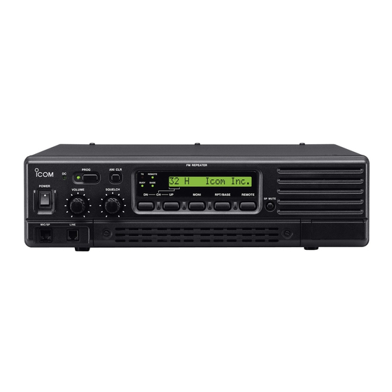
Icom IC-FR4000 Service Manual
Uhf fm repeater
Hide thumbs
Also See for IC-FR4000:
- Service manual (70 pages) ,
- Instruction manual (20 pages) ,
- Price list (158 pages)
Table of Contents
Advertisement
Advertisement
Table of Contents

Subscribe to Our Youtube Channel
Related Manuals for Icom IC-FR4000


Summary of Contents for Icom IC-FR4000
- Page 1 UHF FM REPEATER iC-fr4000 iC-fr4 1 00...
- Page 2 READ the instructions of test equipment thoroughly before connecting equipment to the repeater. Icom, Icom Inc. and are registered trademarks of Icom Incorporated (Japan) in the United States, the United Kingdom, Germany, France, Spain, Russia and/or other countries.
-
Page 3: Table Of Contents
TABLE OF CONTENTS SECTION 1 SPECIFICATIONS SECTION 2 INSIDE VIEWS SECTION 3 CIRCUIT DESCRIPTION 3 - 1 RECEIVER CIRCUITS ....................3 - 1 3 - 2 TRANSMITTER CIRCUITS .................... 3 - 3 3 - 3 PLL CIRCUITS ........................ 3 - 4 3 - 4 OTHER CIRCUITS ...................... - Page 4 SECTION 1 SPECIFICATIONS IC-FR4000 IC-FR4100 Measurement method EIA/TIA-603 ETS 300 086 Low band ([L]; [USA1], [GEN1], [GEN5], [EUR1], [FRG1]): 400.000–430.000 MHz Frequency range Middle band ([M]; [GEN2], [GEN6]): 430.000–450.000 MHz High band ([H]; [USA3], [GEN3], [GEN7], [EUR3], [FRG3]):450.000–480.000 MHz Wide (25 kHz):...
-
Page 5: Inside Views
SECTION 2 INSIDE VIEWS • 25PA UNIT Top view Power amplifier IC2: SC-1323 [H] SC-1322 [L] +10V REG (IC8: µPC2912T) APC amplifier (Q11: 2SB1143, Q12; 2SC2712) YGR amplifier (Q4: 3SK3475) Temp sensor (IC3: NJM2107F D15: MA29WB) +5V REG (IC7: TA78L05F) •... - Page 6 • LOGIC UNIT Top view Ringer detect circuit (IC48: TLP121) DTMF decoder (IC30: TC4W53FU, IC31: LC7387M) CTCSS decoder (IC29: FX805LG) EEPROM (IC37: HN58X2464TI) (IC33: HD64F2238BF) Splatter filter (IC4: NJM2902V) D/A converter (IC25: M62364) Temperature switching circuit (IC32: TC4W53) Mic mix amplifier (IC2: NJM2902V) AF amplifier (IC17: LA4425A)
- Page 7 TX VCO circuit • TX UNIT Top view Mixer (IC6: NJM2107F) D/A converter* (IC5: M62364FP) PLL reference oscillator 12.8 MHz (X1: CR-732 or CR-758) PLL IC* (IC2: MB15A02PFV1) • RX UNIT Top view PLL IC* RF amplifier (IC4: MB15A02PFV1) (Q1: 2SC5337) *: Located under side of this point.
-
Page 8: Circuit Description
SECTION 3 CIRCUIT DESCRIPTION 3-1 RECEIVER CIRCUITS IC2 contains the 2nd mixer, IF amplifier, quadrature detec- tor, active filter and noise amplifier circuits, etc. The local 3-1-1 RF CIRCUIT (RX UNIT) oscillator section and X2 generate 69.545 MHz for the 2nd Received signals from the RX antenna connector enter the LO signal. - Page 9 3-1-6 RECEIVER MUTE CIRCUITS (LOGIC UNIT) The CTCSS signal passes through the low-pass filter circuit (IC8, pins 1, 3, 5, 7, 8, 10) and is then applied to the CTCSS • NOISE SQUELCH decoder IC (IC29). The detected signal is applied to the The noise squelch circuit cuts out AF signals when no RF CPU (IC33) via the serial signal line.
-
Page 10: Transmitter Circuits
RPT AF mute switch (IC14), and are nal to the level needed at the power amplifier. applied to the limiter amplifier (IC3). • IC-FR4000 (50PA UNIT) • IN CASE OF THE 2/5TONE SIGNALS The RF signal from the TX unit pass through the attenuator The 2/5TONE signals from the CPU (IC33, pin 43) are circuit (R12–R14), the low-pass filter circuit (L1, L13, C3,... - Page 11 3-2-4 POWER AMPLIFIER CIRCUIT 3-2-5 APC CIRCUIT (50PA OR 25PA UNIT) (50PA OR 25PA UNIT) • IC-FR4000 (50PA UNIT) The APC circuit protects the power amplifier from a mis- The power amplifier circuit amplifies the driver signal to an matched output load and stabilizes the output power.
-
Page 12: Pll Circuits
3-3 PLL CIRCUITS 3-3-5 TRANSMITTER PLL CIRCUIT (TX UNIT) The PLL IC (IC2) which includes in the prescaler, the pro- 3-3-1 GENERAL grammable counter and the phase comparator. The PLL IC Each receiver and transmitter circuit has an independent sets the divided ratio which bases on N-data from the CPU PLL circuit for controlling frequencies. -
Page 13: Power Supply Circuits
3-5 POWER SUPPLY CIRCUITS AF signals from J13 (FRONT unit) are applied to the network 3-5-1 LOGIC AND REG UNITS VOLTAGE LINES IC (IC46). The output signals from IC46 (pins 8, 9) are Line Description applied the AF amplifier IC (IC1, pin 2) via “T8” signal. The signals pass through the MIC mute switch, the MIC mixer The voltage from the DC power unit (CHASSIS;... -
Page 14: Port Allocations
3-6 PORT ALLOCATIONS 3-6-3 EXPANDER IC (LOGIC UNIT; IC41) 3-6-1 EXPANDER IC (LOGIC UNIT; IC39) Port Description number name Port Description number name Outputs the switch control signal for R/BSW the received AF signal to the micro- Outputs the control signal for “BASE” BASL phone amplifier. - Page 15 3-6-5 D/A CONVERTER IC (TX UNIT; IC5) 3-6-6 CPU (LOGIC UNIT; IC33) Port Port Description Description number name number name Input port for the TONE signal from Outputs the strobe signal for the PLL ETONE RPLSTB the ACC connector. IC on the RX unit. Outputs the adjusted external TONE Outputs the strobe signal for the PLL ETONEO...
- Page 16 CPU-Continued CPU-Continued Port Port Description Description number name number name Input port for the RV SWR signal from Outputs the strobe signal for the port RVSWR PE3STB the PA unit. expander IC (LOGIC unit; IC41). Input port for the temperature signals Outputs the strobe signal for the port TEMP PE2STB...
-
Page 17: Adjustment Procedures
SECTION 4 ADJUSTMENT PROCEDURES 4-1 PREPARATION Some adjustments must be performed on the “ADJUSTMENT MODE”. CS-FR3000 , OPC-478 CLONING SOFTWARE CLONING , OPC-592 are required when enter the adjustment mode. Refer to the next page in detail. CABLE ADAPTOR CABLE I REQUIRED TEST EQUIPMENT EQUIPMENT GRADE AND RANGE... - Page 18 I BEFORE ENTERING THE ADJUSTMENT MODE CAUTION!: Need to back up the original memory data using CS-FR3000 before cloning the adjustment frequencies. When program the adjustment frequencies into the repeater, the repeater’s memory channels will be overwritten the data and deleted original memory data at the same time. Need to do cloning “Adjustment Mode Access”...
- Page 19 I ENTERING THE ADJUSTMENT MODE [CH-DN] 1 Turn the power OFF. [POWER] [CH-UP] 2 While pushing and holding both [CH-DN] and [CH-UP], turn ON. NEVER release [CH-DN] and [CH-UP] until 1 short beep sounds. 3 Push [CH-DN] button, then sounds 2 beep audio. I OPERATING IN THE ADJUSTMENT MODE •...
- Page 20 ADJUSTMENT MODE FREQUENCY LIST [USA3], [GEN3], [USA1], [GEN1], [GEN2], [GEN6] [GEN7], [EUR3], [GEN5], [EUR1], LCD DISPLAY ADJUSTMENT [FRG3] (MHz) [FRG1] (MHz) (MHz) A01 LW TXREF 127 TVCO/RVCO adjustment. 429.925 (RX) 449.925 (RX) 479.925 (RX) Reference frequency adjustment. 400.275 (TX) 430.275 (TX) 450.275 (TX) A02 LW HRTUN 115 NONE...
-
Page 21: Pll Adjustmenst
4-2 PLL ADJUSTMENT MEASUREMENT ADJUSTMENT ADJUSTMENT ADJUSTMENT CONDITIONS VALUE UNIT LOCATION UNIT ADJUST : A01 LW TXREF 127 1.0 V TX VCO LOCK • LCD display Connect the digital TVCO VOLTAGE • Receiving multi meter or oscillo- 0.8 V scope to check point CP1. -
Page 22: Receiver Adjustment
4-3 RECEIVER ADJUSTMENT MEASUREMENT ADJUSTMENT ADJUSTMENT ADJUSTMENT CONDITIONS VALUE UNIT LOCATION UNIT ADJUST : A03 LW MRTUN 083 • LCD display Connect the digital Maximum C10, • Connect the standard signal generator SENSITIVITY multi meter or oscillo- voltage C11, to the [RX] antenna connector and set scope to check point C12, CP18. -
Page 23: Software Adjustment
4-4 SOFTWARE ADJUSTMENT Select an item using [CH-UP] / [CH-DN] buttons, then set specified value using [RPT/BASE] / [MONI] buttons on the FRONT PANEL. MEASUREMENT ADJUSTMENT ADJUSTMENT CONDITION VALUE UNIT LOCATION : A06 HW POWER OUTPUT Rear Connect the RF power meter to 50.0 W [FR4000] •... - Page 24 SOFTWARE ADJUSTMENT – continued Select an item using [CH-UP] / [CH-DN] buttons, then set specified value using [RPT/BASE] / [MONI] buttons on the FRONT PANEL. MEASUREMENT ADJUSTMENT ADJUSTMENT CONDITION VALUE UNIT LOCATION : A10 LW CTCDEV CTCSS Rear Connect the FM deviation meter ±0.7 kHz •...
- Page 25 SOFTWARE ADJUSTMENT – continued Select an item using [CH-UP] / [CH-DN] buttons, then set specified value using [RPT/BASE] / [MONI] buttons on the FRONT PANEL. MEASUREMENT ADJUSTMENT ADJUSTMENT CONDITION VALUE UNIT LOCATION : A13 LW RPTAF ±3.0 kHz 1, 2, 3 REPEATER Rear Connect the FM deviation meter...
-
Page 26: Parts List
SECTION 5 PARTS LIST [REG UNIT] [REG UNIT] ORDER ORDER DESCRIPTION DESCRIPTION 1180001320 NJM7809FA 4030006900 S.CERAMIC C1608 JB 1H 103K-T 1180002290 S.IC NJTM7809DL1A-TE 4030006860 S.CERAMIC C1608 JB 1H 102K-T 1180001860 S.IC TA78M05F (TE16L) 4510007660 ELECTROLYTIC LXZ25VB100 1180002480 S.REG TA78DL12AF (TE16L) 4510007660 ELECTROLYTIC LXZ25VB100... -
Page 27: Front Unit
[FRONT UNIT] [FRONT UNIT] ORDER ORDER DESCRIPTION DESCRIPTION 1530002060 S.TRANSISTOR 2SC4081 T106 R 6910014560 SPACER LM-15 6910014550 SPACER LM-13 6910014540 SPACER LM-10 1750000930 S.DIODE NNCD8.2C-T1 6910014540 SPACER LM-10 1750000930 S.DIODE NNCD8.2C-T1 6910014540 SPACER LM-10 1750000930 S.DIODE NNCD8.2C-T1 6910014540 SPACER LM-10 6200001620 S.COIL ELJFC 1R0K-F... - Page 28 [LOGIC UNIT] [LOGIC UNIT] ORDER ORDER DESCRIPTION DESCRIPTION ERJ3GEYJ 271 V (270 Ω) 1590002430 S.TRANSISTOR DTA144EE TL 7030003370 S.RESISTOR 1510000590 S.TRANSISTOR 2SA1362-Y (TE85L) 7030003600 S.RESISTOR ERJ3GEYJ 223 V (22 kΩ) 1160000150 S.TRANSISTOR IMZ4 T108 7030003680 S.RESISTOR ERJ3GEYJ 104 V (100 kΩ) 1590001960 S.TRANSISTOR XP4311 (TX)
- Page 29 [LOGIC UNIT] [LOGIC UNIT] ORDER ORDER DESCRIPTION DESCRIPTION R143 7030000410 S.RESISTOR MCR10EZHJ 1.8 kΩ R242 7030003680 S.RESISTOR ERJ3GEYJ 104 V (100 kΩ) R144 7030000480 S.RESISTOR MCR10EZHJ 6.8 kΩ R243 7030003680 S.RESISTOR ERJ3GEYJ 104 V (100 kΩ) R145 7030000410 S.RESISTOR MCR10EZHJ 1.8 kΩ R245 7030003570 S.RESISTOR...
- Page 30 [LOGIC UNIT] [LOGIC UNIT] ORDER ORDER DESCRIPTION DESCRIPTION R370 7030003480 S.RESISTOR ERJ3GEYJ 222 V (2.2 kΩ) R520 7030003620 S.RESISTOR ERJ3GEYJ 333 V (33 kΩ) R371 7030003640 S.RESISTOR ERJ3GEYJ 473 V (47 kΩ) R521 7030003640 S.RESISTOR ERJ3GEYJ 473 V (47 kΩ) ERJ3GEYJ 100 V (10 Ω) R372 7030003200...
- Page 31 [LOGIC UNIT] [LOGIC UNIT] ORDER ORDER DESCRIPTION DESCRIPTION 4030006860 S.CERAMIC C1608 JB 1H 102K-T C182 4030007090 S.CERAMIC C1608 CH 1H 470J-T 4030017490 S.CERAMIC C1608 JB 1A 105K-T C184 4030007090 S.CERAMIC C1608 CH 1H 470J-T 4030011600 S.CERAMIC C1608 JB 1E 104K-T C185 4030007090 S.CERAMIC...
- Page 32 [LOGIC UNIT] [LOGIC UNIT] ORDER ORDER DESCRIPTION DESCRIPTION C290 4510004630 S.ELECTROLYTIC ECEV1CA100SR C440 4030011600 S.CERAMIC C1608 JB 1E 104K-T C292 4550006250 S.TANTALUM TEESVA 1A 106M8L C441 4030018060 S.CERAMIC C5750 JB 2E 474KT C294 4550006250 S.TANTALUM TEESVA 1A 106M8L C442 4030017490 S.CERAMIC C1608 JB 1A 105K-T C295...
- Page 33 [RX UNIT] [RX UNIT] ORDER ORDER DESCRIPTION DESCRIPTION 1190000450 S.IC GN2011-Q (TX) 6910011690 S.COIL ACB1608M-600-T 1110003490 S.IC TA31136FN (D,EL) 6910011690 S.COIL ACB1608M-600-T 1180000420 S.IC TA78L05F (TE12R) 6910011690 S.COIL ACB1608M-600-T 1140005990 S.IC MB15A02PFV1-G-BND-ER 6200007680 S.COIL LQW2BHN12NJ01L 1110002750 S.IC TA75S01F (TE85R) 6200007680 S.COIL LQW2BHN12NJ01L 1180000420...
- Page 34 [RX UNIT] [RX UNIT] ORDER ORDER DESCRIPTION DESCRIPTION ERJ3GEYJ 330 V (33 Ω) R136 7030003260 S.RESISTOR 4030006990 S.CERAMIC C1608 CH 1H 080D-T [FR4100] [GEN2], [GEN6], [EUR3], [FRG3] ERJ3GEYJ 680 V (68 Ω) 7030003300 S.RESISTOR 4030009910 S.CERAMIC C1608 CH 1H 040B-T Other [FR4000] 4610001590...
- Page 35 [RX UNIT] [RX UNIT] ORDER ORDER DESCRIPTION DESCRIPTION C137 4030006860 S.CERAMIC C1608 JB 1H 102K-T C225 4030006860 S.CERAMIC C1608 JB 1H 102K-T C138 4030006860 S.CERAMIC C1608 JB 1H 102K-T [EUR3], [FRG3] C140 4510004640 S.ELECTROLYTIC ECEV1CA470SP 4030009530 S.CERAMIC C1608 CH 1H 030B-T [L], [M] C141 4030006860...
- Page 36 [RVCO UNIT] [TX UNIT] ORDER ORDER DESCRIPTION DESCRIPTION 1560001280 S.FET 2SK508 K53 T1B 1180000420 S.IC TA78L05F (TE12R) 1530002920 S.TRANSISTOR 2SC4226-T1 R25 1140005990 S.IC MB15A02PFV1-G-BND-ER 1110002400 S.IC NJM2107F-TE1 1180000430 S.IC TA78L06F (TE12L) 1720000640 S.VARICAP 1SV284 (TPH3) 1190001350 S.IC M62364FP 600D 1720000640 S.VARICAP 1SV284 (TPH3) 1110002400...
- Page 37 [TX UNIT] [TX UNIT] ORDER ORDER DESCRIPTION DESCRIPTION 7030003520 S.RESISTOR ERJ3GEYJ 472 V (4.7 kΩ) 4030007010 S.CERAMIC C1608 CH 1H 100D-T 7030003480 S.RESISTOR ERJ3GEYJ 222 V (2.2 kΩ) 4030006860 S.CERAMIC C1608 JB 1H 102K-T ERJ3GEYJ 680 V (68 Ω) 7030003300 S.RESISTOR 4030006860 S.CERAMIC...
- Page 38 ORDER DESCRIPTION DESCRIPTION 1530000371 S.TRANSISTOR 2SC3356-T1B R25 1110002750 S.IC TA75S01F (TE85R) 1530002920 S.TRANSISTOR 2SC4226-T1 R25 1150001670 S-AU27AL (ICOM) / SC-1322 [L] 1150001680 S-AU27AM (ICOM) / SC-1323 [H] 1110002400 S.IC NJM2107F-TE1 1720000640 S.VARICAP 1SV284 (TPH3) 1180000420 S.IC TA78L05F (TE12R) 1720000640 S.VARICAP...
- Page 39 [25PA UNIT] IC-FR4100 ONLY [25PA UNIT] IC-FR4100 ONLY ORDER ORDER DESCRIPTION DESCRIPTION 7030003440 S.RESISTOR ERJ3GEYJ 102 V (1 kΩ) C109 4550006470 S.TANTALUM TEESVB2 1D 106M8L 7030003550 S.RESISTOR ERJ3GEYJ 822 V (8.2 kΩ) C111 4030011600 S.CERAMIC C1608 JB 1E 104K-T ERJ3GEYJ 101 V (100 Ω) 7030003320 S.RESISTOR C112...
- Page 40 [50PA UNIT] IC-FR4000 ONLY [50PA UNIT] IC-FR4100 ONLY ORDER ORDER DESCRIPTION DESCRIPTION 1150000180 M57729 / SC1027 7030003560 S.RESISTOR ERJ3GEYJ 103 V (10 kΩ) MCR10EZHJ 22 Ω (220) 1150001670 S-AU27AL (ICOM) / SC-1322 [L] 7030000180 S.RESISTOR ERJ3GEYJ 101 V (100 Ω)
- Page 41 [50PA UNIT] IC-FR4000 ONLY [VARISTOR UNIT] IC-FR4000 ONLY ORDER ORDER DESCRIPTION DESCRIPTION 4030006860 S.CERAMIC C1608 JB 1H 102K-T 1790000720 DIODE MA29W-B 4030006850 S.CERAMIC C1608 JB 1H 471K-T 4030006850 S.CERAMIC C1608 JB 1H 471K-T 4030006860 S.CERAMIC C1608 JB 1H 102K-T 6910012350 S.BEAD...
-
Page 42: Vr Unit
[JACK2 UNIT] [VR UNIT] ORDER ORDER DESCRIPTION DESCRIPTION 1750000930 S.DIODE NNCD8.2C-T1 7210003110 VARIABLE RK0971110 10KA 1750000930 S.DIODE NNCD8.2C-T1 7210003120 VARIABLE RK0971110 10KB 1750000930 S.DIODE NNCD8.2C-T1 1750000930 S.DIODE NNCD8.2C-T1 1750000930 S.DIODE NNCD8.2C-T1 6510018950 S.CONNECTOR B7B-PH-SM3-TB 1750000930 S.DIODE NNCD8.2C-T1 1750000930 S.DIODE NNCD8.2C-T1 1750000930 S.DIODE NNCD8.2C-T1... -
Page 43: Voice Scrambler Unit
SECTION 6 OPTION UNIT INSTALLATION 6-1 Opening the repeater’s case Follow the case and cover opening procedures shown here when an optional unit is installed or adjust the in- ternal units, etc. CAUTION: DISCONNECT the AC power cable and/or DC power cable from the repeater. Other- wise, there is danger of electric shock and/or equip- ment damage. - Page 44 6 Unplug the TX ANT–PA unit cable from the TX ANT 6-3 Duplexer and isolater connecter (CHASSIS), and then plug to the isolater installation (input connector). q Remove the top and bottom covers (See page 6-1). w Tighten 4 screws, A, for installing the duplexer unit. 3 Tighten 4 screws, B, for installing the isolater unit.
- Page 45 CONNECTION EXAMPLE 1 : ISOLATER CONNECTION EXAMPLE 2 : DUPLEXER CONNECTION EXAMPLE 3: DUPLEXER AND ISOLATER CONNECTION DUP: DUPLEXER ISO: ISOLATER 6 - 3...
- Page 46 SECTION 7 MECHANICAL PARTS AND DISASSEMBLY [CHASSIS PARTS] [LOGIC UNIT] ORDER ORDER QTY. QTY. DESCRIPTION DESCRIPTION 8900011521 OPC-1049A (Power SW cable) 6910015390 FRC27-12-1.3 [FR4100] only 8900011571 OPC-1055A (LOGIC-JACK2 cable A) 6910015390 FRC27-12-1.3 [FR4100] only 8900011580 OPC-1056 (LOGIC-JACK2 cable B) 6910014890 FRC-WC1 [FR4100] only 8900011590...
- Page 47 MP17 MP84 FRONT UNIT MP84 MP82 W5 (L) EP2 (F) MP69 MP84 JACK1 UNIT MP82 W4 (L) MP84 MP68 EP3 (F) MP82 MP16 EP4 (F) EP7 (F) MP84 MP86 MP68 EP6 (F) MP82 MP27 EP5 (F) MP10 MP84 MP68 MP86 MP85 MP68 MP69...
-
Page 48: Tvco Unit
MP64 MP63 MP64 MP63 (25PA) MP100 (25PA) (25PA) (25PA) MP18 (25PA) [EUR3] [EUR1] [FRG3] [FRG1] MP64 MP64 MP90 MP90 MP100 (25PA) MP64 MP90 MP64 MP54 MP55 MP54 MP55 25PA UNIT MP58 MP90 MP64 MP74 (25PA) MP64 MP53 (25PA) MP74 MP90 MP90 MP53 to EP7 (R) - Page 49 [CHASSIS PARTS] [RX UNIT] ORDER ORDER QTY. QTY. DESCRIPTION DESCRIPTION 8510015120 2368 A-case 6510022970 Connector N-PA-JJ(NI) 8510015130 2368 B-case 8510015140 2368 E-case 8900011510 OPC-1048 (AC input cable) 8930059680 Sponge (HD) 8900011521 OPC-1049A (Power SW cable) 8930059680 Sponge (HD) 8900011531 OPC-1050A (Back up DC cable) 8510015190 2368 MCF plate 8900011540...
- Page 50 SECTION 8 SEMI-CONDUCTOR INFORMATION 8 - 1 TRANSISTORS AND FETS 8 - 2 DIODES 2SA1362-Y 2SA1576A T106R 2SB1143 T 2SB1182 TL Q 2SC2712-BL/GR 1SR154-400 TE25 1SS226 (TE85R) 1SS268 (TE85R) 1SS319 (TE85R) 1SS355 TE-17 (Symbol: AEY) (Symbol: FR) (Symbol: B1143 (Symbol: B1182, Q) (Symbol: LL/LG) (Symbol: 14) (Symbol: C3)
- Page 51 SECTION 9 BOARD LAYOUTS The combination of this page and the next page shows the unit layout in the same configuration as the actual P.C. Board. 9 - 1 FRONT UNIT ¡TOP VIEW to LCD DS7 9 - 2 VR UNIT 9 - 3 TVCO UNIT 9 - 4 RVCO UNIT ¡TOP VIEW...
- Page 52 FRONT UNIT ¡BOTTOM VIEW to LOGIC UNIT J4 The combination of this page and the previous page shows the unit layout in the same configuration as the to LOGIC UNIT J3 actual P.C. Board. to LOGIC UNIT – to JACK1 UNIT J3 TVCO UNIT VR UNIT...
- Page 53 9 - 5 LOGIC UNIT The combination of this page and the next page shows the ¡ ¡ TOP VIEW unit layout in the same config- uration as the actual P.C. to JACK1 UNIT J3 to JACK2 UNIT J2 to JACK2 UNIT J3 Board.
-
Page 54: Logic Unit
to OPTIONAL UNIT to OPTIONAL UNIT LOGIC UNIT The combination of this page and the previous page shows ¡ ¡ BOTTOM VIEW the unit layout in the same con- figuration as the actual P.C. Board. SDTO RPLSTB to RX UNIT J2 RUNLK W/NS RSSI... - Page 55 9 - 6 RX UNIT ¡ ¡ TOP VIEW RX ANT The combination of this page and the next page shows the unit lay- out in the same configuration as the actual P.C. Board. RX OUT to LOGIC UNIT J1 9 - 5...
-
Page 56: Rx Unit
¡ ¡ BOTTOM VIEW RX UNIT The combination of this page and the previous page shows the unit layout in the same configuration as RX ANT the actual P.C. Board. 9 - 6... - Page 57 9 - 7 TX UNIT The combination of this page and the next page shows to 25PA/50PA UNIT the unit layout in the same configuration as the actual ¡ ¡ TOP VIEW P.C. Board. to LOGIC UNIT J2 FWSWR RVSWR PATEMP TMUTE2 ETONE...
-
Page 58: Tx Unit
TX UNIT The combination of this page and the previous page shows the unit layout in the same configuration as the ¡ ¡ BOTTOM VIEW actual P.C. Board. 9 - 8... - Page 59 9 - 8 50PA UNIT [FR4000] The combination of this page and the next page shows the unit layout in the same configuration as the actual ¡ ¡ TOP VIEW P.C. Board. C125 C18 C126 1 2 3 TX ANT 9 - 9 VARISTER UNIT [FR4000] ¡TOP VIEW to REG UNIT...
-
Page 60: 50Pa Unit [Fr4000]
50PA UNIT [FR4000] The combination of this page and the previous page shows the unit layout in the same configuration as the ¡ ¡ BOTTOM VIEW actual P.C. Board. VARISTER UNIT [FR4000] ¡BOTTOM VIEW 9 - 10... - Page 61 9 - 10 25PA UNIT [FR4100] The combination of this page and the next page shows the unit layout in the same configuration as the actual ¡ ¡ TOP VIEW P.C. Board. TX ANT to REG UNIT to REG UNIT to TX UNIT J5 to TX UNIT J4 9 - 11...
-
Page 62: 25Pa Unit [Fr4100]
25PA UNIT [FR4100] The combination of this page and the previous page shows the unit layout in the same configuration as the ¡ ¡ BOTTOM VIEW actual P.C. Board. 9 - 12... - Page 63 AC IN 9 - 11 REG UNIT POWER The combination of this page and the next to LOGIC UNIT J6 PS 0V page shows the unit layout in the same BATTERY ¡ ¡ TOP VIEW DC SUPPLY PS 15V configuration as the actual P.C. Board. to LOGIC to PA FAN to REG FAN...
-
Page 64: Reg Unit [Fr4000]
REG UNIT The combination of this page and the pre- vious page shows the unit layout in the ¡BOTTOM VIEW same configuration as the actual P.C. Board. to 25PA/ to 25PA/ BATTERY BATTERY 50PA UNIT 50PA UNIT – PS 15V PS 15V PS 0V PS 0V... -
Page 65: Jack1 Unit [Fr4100]
9 - 14 JACK1 UNIT [FR4100] The combination of this page and the next page shows the unit layout in the same ¡TOP VIEW configuration as the actual P.C. Board. SP JACK MODULAR JACK to LOGIC UNIT J9 to FRONT UNIT J9 9 - 15 JACK2 UNIT [FR4100] ¡TOP VIEW... - Page 66 JACK1 UNIT [FR4100] The combination of this page and the previous page shows the unit layout in the same configuration as the ¡BOTTOM VIEW actual P.C. Board. JACK2 UNIT [FR4100] ¡BOTTOM VIEW to LOGIC UNIT J10 9 - 16...
-
Page 67: Block Diagram
SECTION 10 BLOCK DIAGRAM IC4D: NJM2902V SCK,SDTO,DA1STB,TPLSTB Q1: XP1214 CTDTO TONE IC13: BU4066BCFV IC2A, B: IC4A, B, C: from CPU TUNLK IC1D: NJM2902V IC2D: NJM2902V IC2C: NJM2902V NJM2902V IC3A: NJM2902V IC3B: NJM2902V NJM2902V MIC MUTE PATEMP PRE- SPLAT SW-D LIMIT FWSWR RVSWR MICMUTE1... - Page 68 IC2: SC-1322[L] SC-1323[H] Q4: 2SK3475 Q7: DTC114EU D2: HSU88 VCC1 Q8: 2SA1362 D4: HSU88 Q9: DTC114EU Q10: DTC114EU Q11: 2SB1143 IC8: µPC2912T Q12: 2SC2712 IC1: TA75S01F +10V +10V VCC1 TMUTE2 PCON CTRL IC1: TA78L05F IC7: TA78L05F D15: MA29W B TMUTE2 TMUTE2 PCON 25PA UNIT...
- Page 69 SECTION 11 WIRING DIAGRAM DISPLAY W4 (LOGIC) REMOTE RX UNIT SPMUTE MICE CLONE W10 (LOGIC) <W18 (CHASSIS), W19 (CHASSIS)> M PTT to SP MIC RVCO MICE CLONE UNIT M PTT M MONI M MONI SDTO RPLSTB RX OUT W17 (CHASSIS) RUNLK W/NS TELG...
- Page 70 SECTION 12 VOLTAGE DIAGRAM REMOTE REMOTE SP MUTE FREE: 4.7V SPMUTE PUSH: 0.0V S7 SKQDPB S8 SKQDPB MICE 5.0V 3.8V to LOGIC UNIT J4 CLONE M PTT M MONI REMOTE SP MUTE REP/BASE MONI MSC-C161UYLY-4W FREE: 4.2V PUSH: 0.0V S6 SKQDPB S5 SKQDPB 0.001 [FR4100] Q1 2SC4081...
- Page 71 W23* W27* 4p [USA3], [GEN3], 4p [USA3], [GEN3], 4p [USA3], [GEN3], 4p [USA3], [GEN3], 0.001 0.27µH [FR4100] W24* W28* [GEN7] [GEN7] [GEN7] [GEN7] 3.3k 22nH 4p [other] 0.22µH [FR4000] 5p [EUR3], [FRG3] 5p [EUR3], [FRG3] 5p [EUR3], [FRG3] 5p [EUR3], [FRG3] 3.5V 8p [GEN2], [GEN6] 0.001...
- Page 72 WS1 [FR4000] TVCO UNIT 1µH to 50PA UNIT R101 W11 [FR4100] 18 [L], [M], [FR4100] C123 to 25PA UNIT 0.001 100p 2SC3356 100p 0.001 15nH 0.001 JPW [USA3], [GEN3], [GEN7] 1SV308 22nH 22nH 0.001 7.9V 2SC4703 2.6V 0.6V R100 R102 100p 18nH 1p [M], [H]...
- Page 73 AC IN CHASSIS UNIT POWER FP2152A [100-120V] FP2153A [220-240V] PS 0V PS 0V DC SUPPLY PS 15V M SW PS 0V EP10 ATC-20 PS 15V PS 15V PS 15V M SW PS 0V FCH30A03L TA78L08F PS 15V PS 0V PS 15V 2SJ533 0.001 0.001...
- Page 74 C383 22p C366 R453 10 LIMIT S MIX IC4A IC4C IC2A SPLATTER FILTER IC3A MIC MIX PRE-EMP IC2C IC2B IC13 NJM2902V NJM2902V C380 2.5V NJM2902V IC3B 5.0V R497 NJM2902V R23 330k R118 NJM2902V NJM2902V BU4066BCFV 4.7k 100k NJM2902V 2.0V C408 1.9V C364 C382...
- Page 75 Mount B-Side to RX UNIT J2 to TX UNIT J3 to FRONT UNIT J2 to FRONT UNIT J1 1 2 3 4 5 6 7 8 9 10 11 12 13 14 15 16 17 18 19 20 21 22 1 2 3 4 5 6 7 8 9 10 11 12 13 14 15 16 17 18 19 20 21 22 13.6V L4 BLM31PG121SN1...
- Page 76 [FR4000] SC-1027 [M] SC-1322 [L] SC-1323 [H] 470p 0.001 470p C119 C126 C125 2p [L], [M] 470p 4p [H] C112 100p 6p [H] LA-559 LA-559 LA-560 TXRFOUT 8p [M] TX ANT 7p [L] 2SC3102 Y655LY-03K=P3 Y655LY-01M 0.001 100p TXRFIN 0.001 470p 0.001 to TX UNIT...
- Page 77 [FR4100] SC-1322 [L] NJM2107F SC-1323 [H] 100k 0.001 BLM31PG121SN1 3.5V 2.8V C130 470p 1.2k MA29W C134 C127 C129 BL01RN1A1D2B 5.0V 3.9k BLM31PG121SN1 0.001 470p to REG UNIT LA-563A 13.1V LA-563A BEADS VCC1 C108 (CHASSIS) 0.01 470p 0.001 TC-7 BEADS 470p 0.001 C107 C105...
- Page 78 Unit 9, Sea St., Herne Bay, Kent, CT6 8LD, U.K. Phone : +44 (01227) 741741 Fax : +44 (01227) 741742 : http://www.icomuk.co.uk Icom (Australia) Pty. Ltd. E-mail : info@icomuk.co.uk A.B.N. 88 006 092 575 290-294 Albert Street, Brunswick, Victoria, 3056, Australia Icom France S.a...
- Page 79 S-13913MZ-C1-2 1-1-32, Kamiminami, Hirano-ku, Osaka, 547-0003, Japan © 2003–2004 Icom Inc.
Need help?
Do you have a question about the IC-FR4000 and is the answer not in the manual?
Questions and answers