Sanyo VCC-6585P Service Manual
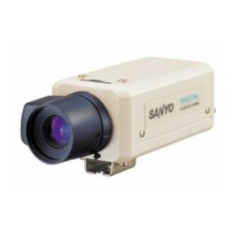
Color ccd camera
Hide thumbs
Also See for VCC-6585P:
- Brochure (18 pages) ,
- Instruction manual (2 pages) ,
- Service manual (27 pages)
Table of Contents
Advertisement
Quick Links
Notice
CORRECTION
SERVICE FLASH
Please add this notice to the Service manual listed below.
Category : COLOR CCD camera
Model Name
VCC-6585P
The reason of change.
A : Misprint
E : Deletion
REASON : D (Design)
Refer to this notice for the service manual for products with a serial number of 94511001 or
later. (Product Code : 117 136 08 and 117 300 03, An "R" appears at the end of the serial
number)
Refer to the service manuals and notices that have been issued previously for products with
a serial number that is earlier than 94511001.
CONTENTS
1. DISASSEMBLY ....................................4
2. BOARD LOCATION ............................. 5
3. ADJUSTMENT ..................................... 6
4. PARTS LIST .........................................9
WARNING
This product has been manufactured using lead-free solder. Be sure to follow the warning given on page 2 when carrying out
repair work.
The components designated by a symbol ( ! ) in this schematic diagram designates components whose value are of
part designated in the Parts List. Do not deviate from the resistance, wattage, and voltage ratings shown.
NOTE : 1. Parts order must contain model number, part number, and description.
2. Substitute parts may be supplied as the service parts.
3. N. S. P. : Not available as service parts.
Design and specification are subject to change without notice.
L5AX2/XE,XEG,XEC1P,XEGC1P
117 136 01,08, 117 300 01,03
PRODUCTION CHANGE
ADD INFORMATION
Reference No.
SM5310593
B : Quality Reliability
F : Addition
PRODUCT SAFETY NOTICE
SANYO Electric Co., Ltd.
Osaka,Japan
Destination
Europe, China, PAL General
C : Standardization
G : Multiple Use
- 1 -
FILE No.
Date : 13 Jan. 2006
D : Design
Reference No. SM5310593-01
Advertisement
Chapters
Table of Contents

Related Manuals for Sanyo VCC-6585P


Summary of Contents for Sanyo VCC-6585P
-
Page 1: Table Of Contents
2. Substitute parts may be supplied as the service parts. 3. N. S. P. : Not available as service parts. Design and specification are subject to change without notice. SANYO Electric Co., Ltd. Reference No. SM5310593-01 L5AX2/XE,XEG,XEC1P,XEGC1P 117 136 01,08, 117 300 01,03 Osaka,Japan –... - Page 2 WARNING Note: Do not use solder containing lead. If replacing existing solder containing lead with lead-free This product has been manufactured using lead-free solder in the soldered parts of products that have been solder in order to help preserve the environment. manufactured up until now, remove all of the existing solder Because of this, be sure to use lead-free solder when at those parts before applying the lead-free solder.
-
Page 3: Specifications
SPECIFICATIONS Scanning system : PAL standard TV system (625 TV lines, 25 frames/sec.) Interlace : PLL 2:1 interlace Image device : Interline transfer method, 1/3-inch solid-state image device CCD Number of effective pixels : 752 (Horizontal) x 582 (Vertical) Sync system : Internal sync/Line lock (only when using an AC 24 V adaptor) Resolution : 520 TV lines horizontally, 400 TV lines vertically Video output terminal : 1.0 Vp-p/75 Ω, BNC, composite Image S/N ratio : More than 48 dB (More than 50 dB for AGC OFF) -
Page 4: Disassembly
1. DISASSEMBLY 1. Four screws 2 x 4 19. Four screws 2 x 5 2. Two screws 3 x 4 20. Connector 3. Cover top 21. CA-2 board 22. CA-3 board 4. Two screws 3 x 6 23. Two screws 2 x 7 5. -
Page 5: Board Location
2. BOARD LOCATION CN205 VR302 VR322 VR303 VR301 CT232 S3002 CA-3 board (Side A) CA-2 board TP232 TP221 CT221 CA-4 board CA-3 board CA-2 board (Side B) CA-1 board – 5 –... -
Page 6: Adjustment
3. ADJUSTMENT 3-1. ADJUSTMENT CONDITION 3-3-1. Computer screen during adjustment 1. Use the 5,100K viewer for the subject. VHJ-0173 2. Set the trigger signal of oscilloscope to VIDEO OUT, and apply H sync unless specified. SYNC 3. Set each of the S3002 (CA-3) switches to the all OFF posi- tion. - Page 7 3-5. White Balance Adjustment Adjustment location: VR302, VR303 (CA-3) Measuring location: VIDEO OUT Measuring equipment: Oscilloscope, Vectorscope Subject: Color bar chart Adjusting method: 1. Use the “↓” button to be A. IRIS in the adjustment window. 2. Auto iris adjustment will be started automatically. 45 µsec 3.
- Page 8 3-8. Iris Level Adjustment 3-12. Line Phase Adjustment Adjustment location: VR301, S3002-3,4 (CA-3) Adjustment location: S3002-6 (CA-3), VR322 (CA-3) Measuring location: VIDEO OUT Measuring location: VIDEO OUT, 24 V AC/GND terminals Measuring equipment: Oscilloscope Measuring equipment: Oscilloscope Subject: Gray scale chart Adjusting method: Adjusting method: 1.
-
Page 9: Parts List
4. PARTS LIST NOTE : Please refer to this Notice ( SM5310593 - 01 ) for the set since serial number 94511001 or later. (Product Code : 117 136 08 and 117 300 03, An "R" appears at the end of the serial number ) Please refer to Service Manual ( SM5310593 ) for other sets. - Page 10 LOCATION PARTS NO. DESCRIPTION LOCATION PARTS NO. DESCRIPTION L2121 645 055 3134 INDUCTOR,68U J C2514 403 164 0204 CERAMIC 0.1U Z 25V L2131 645 043 7380 INDUCTOR,33U J C2515 403 164 0204 CERAMIC 0.1U Z 25V L2301 645 043 5881 INDUCTOR,10U J C2516 403 382 1809...
- Page 11 LOCATION PARTS NO. DESCRIPTION LOCATION PARTS NO. DESCRIPTION R2526 401 105 7909 MT-GLAZE 0.000 ZA 1/16W R3031 401 038 3504 MT-GLAZE 330 JA 1/10W R2532 401 105 7909 MT-GLAZE 0.000 ZA 1/16W R3032 401 038 3504 MT-GLAZE 330 JA 1/10W R2535 401 105 7909 MT-GLAZE 0.000 ZA 1/16W...
- Page 12 LOCATION PARTS NO. DESCRIPTION LOCATION PARTS NO. DESCRIPTION D4104 407 226 3905 DIODE RSD376 R4301 401 105 7909 MT-GLAZE 0.000 ZA 1/16W 407 199 4909 DIODE 1SS376 (FUSE) D4107 407 218 7706 ZENER DIODE UDZS20B-TE17 F4001 423 031 5200 FUSE 125V 2A D4108 407 207 7700 ZENER DIODE PTZ3.9B...
- Page 13 NJ510 NJ500 5010 5004 NJ500 NJ500 5011 NJ500 NJ610 NJ610 NJ640 6008 6007 5002 8000 6012 8001 NJ530 NJ630 6015 6020(N.S.P.) 6005 NJ600 NJ630 NJ620 6003 NJ600 NJ680 NJ670 NJ650 NJ660 6001 NJ600 8002 6000(N.S.P.) 5001 NJ610 NJ610 5005 NJ540 5008 5009 NJ520...
-
Page 14: Circuit Diagrams & Printed Wiring Boards
CIRCUIT DIAGRAMS & PRINTED WIRING BOARDS TABLE OF CONTENTS OVERALL WIRING, BLOCK DIAGRAM & CIRCUIT DIAGRAMS Page OVERALL WIRING OVERALL CIRCUIT BLOCK DIAGRAM CA-1 CIRCUIT WAVEFORMS CA-1 CIRCUIT IC101, IC102 & IC103 BLOCK DIAGRAMS IC211 & IC251 BLOCK DIAGRAMS CA-2 CIRCUIT WAVEFORMS CA-2 CIRCUIT CA-3 CIRCUIT CA-4 CIRCUIT... -
Page 15: Special Significance To Product Safety. Should Any Component Designated By A Symbol Need To Be Replaced, Use Only The
NOTES: 1. All resistance values in "OHMS" unless otherwise noted. (K=1,000 ; M=1,000,000) µ 2. All capacitance values in " F" unless otherwise noted. µ p=pico farad ; n=nano farad ; ,u or U=micro farad µ 3. All inductance values in " H"... -
Page 16: Overall Wiring, Block Diagram & Circuit Diagrams
OVERALL WIRING, BLOCK DIAGRAM & CIRCUIT DIAGRAMS OVERALL WIRING CA-1 BOARD CCD UNIT CA-4 BOARD CA-3 BOARD IRIS UNIT POWER UNIT CA-2 BOARD CN401 CN203 CN302 AC24V/DC+ SIGNAL PROCESS AC24V/DC- CCD LEV CCD LEV POWER IN S3002 MICROCOMPUTER +3.3V +3.3V &... -
Page 17: Overall Circuit Block Diagram
OVERALL CIRCUIT BLOCK DIAGRAM CA-1 CIRCUIT WAVEFORMS TEST POINT TEST POINT WAVEFORM WAVEFORM LOCATION LOCATION CN202 CAMERA ASIC CCD IN IC251 Q2103, Q2104 VIDEO OUT IC103 CCDI0-9 1-5, 8-12 65-74 YAOUT Y-LPF Y-LPF PROCESS 6MHz 6MHz SEPARATION IC214 H1, H2, RG H1, H2, RG IC101-13 IC101-1... -
Page 18: Circuit
CA-1 CIRCUIT IC101 BLOCK DIAGRAM CN102 (ICX409AK) R1145 +3.3V R1103 CE-C C1113 0.1;F C1112 XSHT (2125) +15V XSG3B XSG3A (NOTE) R1124 H REGISTER XSUB XSG1B XSG1A XSG1 (NOTE : PHOTO SENSOR) IC102 CXD3400N XSG2 V. DRIVER Q1101 2SK443AJ6 CN101 IC102 BLOCK DIAGRAM R1141 CCD OUT R1116... -
Page 19: Circuit Waveforms
IC211 BLOCK DIAGRAM (SCC0021A) CA-2 CIRCUIT WAVEFORMS TEST POINT TEST POINT WAVEFORM WAVEFORM LOCATION LOCATION 74 73 72 71 70 69 68 67 66 65 64 63 62 61 60 59 58 57 56 55 54 53 52 51 IC251-29 IC211-55 HSYNC/ CSYN C 0.5V/div... - Page 20 CA-2 CIRCUIT L2110 C2141 10;J 100;6.3 C2144 22;6.3-T CE-D R2122 C2111 L2121 C2115 68;J 0.01;B C2142 CT-B2 0.1;F Q2102 Q2101 IC214 2SC4081(R) 2SA1576A(R) 18P;CH +15V NJM2274 L2301 10;J CAOUT R2142 VSAG VOUT R2502 C2143 C2145 (0.5%) CMUTE 0.1;F 100;6.3 2125 C2514 CE-D IC235...
-
Page 21: Circuit
CA-2 CIRCUIT [UPPER-LEFT] R2122 C2111 L2121 68;J Q2101 2SA1576A(R) 18P;CH +15V L2301 10;J CAOUT R2502 C2514 IC235 L2504 0.1;F R2318 10;J C2352 120K 4.7;B C2507 0.1;F (3216) R2314 R2312 R2311 100K C2508 PCOHD 0.1;F R2320 R2316 100K 4.7K R2323 R2132 LA6358NM C2510 PCOVD... -
Page 22: Circuit
CA-2 CIRCUIT [UPPER-RIGHT] L2110 C2141 10;J 100;6.3 C2144 22;6.3-T CE-D R2122 C2111 L2121 C2115 68;J 0.01;B C2142 CT-B2 0.1;F Q2102 Q2101 IC214 2SC4081(R) 2SA1576A(R) 18P;CH NJM2274 CAOUT R2142 VSAG VOUT C2143 C2145 (0.5%) CMUTE 0.1;F 100;6.3 2125 C2514 CE-D 0.1;F YC-MIX C2507 75OHM DRIVER... -
Page 23: Circuit
CA-2 CIRCUIT [LOWER-LEFT] CKI1 R2341 X2301 28.375MHZ R2343 L2302 47;J +3.3V R2664 75 74 73 72 71 70 69 68 67 66 65 64 63 62 61 60 59 58 57 56 55 54 53 52 51 CN201 CSYNC CCD OUT VCC1 TEST ADCK... - Page 24 CA-2 CIRCUIT [LOWER-RIGHT] CN205 +3.3V +3.3V R2271 RSIN RS232IN R2272 RS232OUT RSOUT R2273 RESET VDO1 CPURST R2275 R2664 FLDO1 CHIP12 ADJUSTMENT CHIP3(MIR) NC(OPEN) CHIP4(CAS) NC(OPEN) X2401 NC(OPEN) 5MHZ VSS0 NC(OPEN) CN203 VDD1 VSS1 XOUT NC(OPEN) IC241 NC(OPEN) CCD LEV TEST/VPP NC(OPEN) CCDLEV MICRO COMPUTER...
- Page 25 CA-3 CIRCUIT IC323 R3301 R3229 0;1/16Z B-GAIN NJM2406F Q3203 2SA1576A PHASE SHIFT Q3222 R3226 2SC4081 R-GAIN MANUALR C3221 0.01;B R3224 C3223 R3228 (3216) C3226 MANUALB CN304 0.1;F R3034 1AV4J11AD140G VR322 +15V(CCD) Q3044 PHASE CN302 2SC4081 R3231 1.5K 1AV4J11AD240G +3.3V R3046 R3022 4.7K R3043...
- Page 26 CA-4 CIRCUIT CN401 AC24V/DC+ AC24V/DC- CA-4 POWER IN C4-13600/L5AX2-XEG R4001 R4003 4.7K 4.7K R4030 D4016 PS2701A-1L F4001 2A 125V R4002 TOP VIEW D4001 4.7K TLV431 S1ZB20 1AV4L51B4890G D4101 1SR159-200 T4001 +3.3V D4015 Q4014 R4105 R4301 VIN2 2.7K DTC114EUA D4102 1SS376 CN402 C4110 Q4011...
-
Page 27: Printed Wiring Boards (P.w.b.)
PRINTED WIRING BOARDS (P.W.B.) CA-1 BOARD (SIDE A) CA-1 BOARD (SIDE B) Y1002 R1124 C1123 Y1001 R1126 CN102 CN102 IC101 IC101 CN101 IC102 C1116 C1103 R1106 R1101 C1102 R1103 R1145 D1101 C1112 R1141 SIDE-A C1122 L5AX4/US L5AX4/US R1116 R1117 R1118 C1125 Y1003 C1117... - Page 28 CA-3 BOARD (SIDE A) CA-3 BOARD (SIDE B) CA-4 BOARD (SIDE A) CA-4 BOARD (SIDE B) R4126 C4124 R4110 C4126 R4121 R4123 R4122 Q4013 R4004 Q4014 R4120 C4125 C4122 R4106 R4723 R4705 R4728 R4111 Q4771 R4790 R4131 R4724...
Need help?
Do you have a question about the VCC-6585P and is the answer not in the manual?
Questions and answers