Pioneer DJM-400 Service Manual
Pioneer djm-400 dj mixer service manual
Hide thumbs
Also See for DJM-400:
- Operating instructions manual (76 pages) ,
- Operating instructions manual (16 pages)
Table of Contents
Advertisement
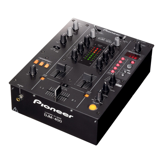
DJ MIXER
DJM-400
THIS MANUAL IS APPLICABLE TO THE FOLLOWING MODEL(S) AND TYPE(S).
Model
Type
DJM-400
KUCXJ
DJM-400
RLXJ
DJM-400
WYXJ5
For details, refer to "Important Check Points for good servicing".
PIONEER CORPORATION
PIONEER ELECTRONICS (USA) INC. P.O. Box 1760, Long Beach, CA 90801-1760, U.S.A.
PIONEER EUROPE NV Haven 1087, Keetberglaan 1, 9120 Melsele, Belgium
PIONEER ELECTRONICS ASIACENTRE PTE. LTD. 253 Alexandra Road, #04-01, Singapore 159936
PIONEER CORPORATION 2006
Power Requirement
AC 120V
AC 110-120V / 220-240V
AC 220-240V
4-1, Meguro 1-chome, Meguro-ku, Tokyo 153-8654, Japan
4
DJM-400
T-IZY MAR. 2006 printed in Japan
ORDER NO.
RRV3351
Remarks
Advertisement
Table of Contents

Related Manuals for Pioneer DJM-400


Summary of Contents for Pioneer DJM-400
- Page 1 PIONEER CORPORATION 4-1, Meguro 1-chome, Meguro-ku, Tokyo 153-8654, Japan PIONEER ELECTRONICS (USA) INC. P.O. Box 1760, Long Beach, CA 90801-1760, U.S.A. PIONEER EUROPE NV Haven 1087, Keetberglaan 1, 9120 Melsele, Belgium PIONEER ELECTRONICS ASIACENTRE PTE. LTD. 253 Alexandra Road, #04-01, Singapore 159936 PIONEER CORPORATION 2006 T-IZY MAR.
-
Page 2: Safety Information
PIONEER Service Manual. A subscription to, or additional copies of, Also test with plug reversed Earth PIONEER Service Manual may be obtained at a nominal (Using AC adapter ground charge from PIONEER. plug as required) - Page 3 To protect products from damages or failures during transit, the shipping mode should be set or the shipping screws should be installed before shipment. Please be sure to follow this method especially if it is specified in this manual. DJM-400...
-
Page 4: Table Of Contents
7.1.1 TEST MODE ............................66 7.1.2 Rewriting of the Software........................72 7.1.3 POWER-ON SEQUENCE ......................... 74 7.1.4 DISASSEMBLY..........................75 7.2 PARTS..............................81 7.2.1 IC ............................... 81 8. PANEL FACILITIES ............................88 8.1 CONNECTION PANEL SECTION......................88 8.2 CONTROL PANEL SECTION ........................89 DJM-400... -
Page 5: Specifications
Microphone equalizer response HI..–12 dB (full counterclockwise) to 0 dB (center) (10 kHz) LOW....–12 dB (full clockwise) to 0 dB (center) (100 Hz) Accessories Power cord (KUCXJ : ADG7021) (RLXJ, WYXJ5 : ADG1154) Operating instructions Warranty card (KUCXJ only) DJM-400... -
Page 6: Exploded Views And Parts List
For the applying amount of lubricants or glue, follow the instructions in this manual. (In the case of no amount instructions, apply as you think it appropriate.) 2.1 PACKING SECTION KUCXJ only DJM-400... - Page 7 Pad A DHA1706 Pad B DHA1707 Pad C DHA1713 Packing Case See Contrast table (2) (2) CONTRAST TABLE DJM-400/KUCXJ, RLXJ and WYXJ5 are constructed the same except for the following: Mark Symbol and Description DRM-400/KUCXJ DRM-400/RLXJ DRM-400/WYXJ5 > Power Cord ADG7021...
-
Page 8: Exterior Section
2.2 EXTERIOR SECTION Refer to "2.3 CONTROL PANEL SECTION". KUCXJ only RLXJ only DJM-400... - Page 9 ICP Cover DNK4625 FCC Label See Contrast table (2) NSP 20 Card Spacer REC1156 (2) CONTRAST TABLE DJM-400/KUCXJ, RLXJ and WYXJ5 are constructed the same except for the following: Mark Symbol and Description DRM-400/KUCXJ DRM-400/RLXJ DRM-400/WYXJ5 JACK Assy DWX2524 DWX2525...
-
Page 10: Control Panel Section
2.3 CONTROL PANEL SECTION JACK CN502 JACK CN500 DJM-400... - Page 11 Level Plate DAH2445 7seg Plate DAH2446 Binder (SKB-909BK) ZCA-SKB90BK Nyron Rivet 3x4.5 RBM-003 Nut M9 DBN1008 • • • • • Screw 3x8 DBA1290 Screw BPZ26P080FTC Screw AMZ30P040FTC Lever SW Stay DNF1740 Fader Stay DNF1746 Screw PMH20P040FTC Screw CMZ26P050FTB DJM-400...
-
Page 12: Block Diagram And Schematic Diagram
3. BLOCK DIAGRAM AND SCHEMATIC DIAGRAM 3.1 BLOCK DIAGRAM 3.1.1 OVERALL BLOCK DIAGRAM DJM-400... -
Page 13: Cpu & Dsp Block Diagram
3.1.2 CPU & DSP BLOCK DIAGRAM DJM-400... -
Page 14: Overall Wiring Diagram
Therefore, when replacing, be sure to use parts of identical designation. ÷ : The power supply is shown with the marked box. CHRV ASSY (DWX2522) 1/3 - VRSW ASSY (DWX2520) FADER ASSY (DWX2521) CFVR ASSY (DWX2523) DJM-400... - Page 15 (RLXJ : DWX2525) (WYXJ5 : DWX2516) CN102 RLXJ : B3P5-VH (3P) KUCXJ, WYXJ5 : B2P3-VH (2P) J3 ( RLXJ) : DKP3745 (3P) J2 (KUCXJ, WYXJ5) : DKP3744 (2P) TRANS ASSY HP ASSY (KUCXJ, WYXJ5 : DWX2519) (DWX2518) (RLXJ : DWX2526) DJM-400...
-
Page 16: Main Assy (1/3)
3.3 MAIN ASSY (1/3) MAIN ASSY (DWX2527) (HP) DJM-400... - Page 17 (HP) : HP L ch IC700 DYW1755 (HD64F3062BFBL25) SYSTEM RESET DJM-400...
-
Page 18: Main Assy (2/3)
3.4 MAIN ASSY (2/3) MAIN ASSY (DWX2527) DC-DC CONVERTER (MICD) (CH2D) (CH1D) IC708 D607A003BRFP200-K (MASTERD) (HPD) DJM-400... - Page 19 (CH1D) : CH 1 Data (CH2D) : CH 2 Data (MICD) : MIC Data (MASTERD) : MASTER Data (HPD) : HP Data SDRAM 64M DJM-400...
-
Page 20: Main Assy (3/3)
3.5 MAIN ASSY (3/3) MAIN ASSY (DWX2527) (CH1) (CH2) A/D CONVERTER for CH1 (CH1D) D/A CONVERTER for MASTER (MASTER) (MIC2) (MIC1) (CH2) (HPD) (MASTERD) (CH1) CN503 DJM-400... - Page 21 : MIC Data (MASTERD) : MASTER Data (HPD) : HP Data (MASTER) : MASTER L ch (HP) : HP L ch A/D CONVERTER for CH2 A/D CONVERTER for MIC/AUX (CH2D) (MICD) (HP) (MASTER) D/A CONVERTER for H.P (HP) (HPD) (HPD) DJM-400...
-
Page 22: Jack Assy (1/4)
REPLACE ONLY WITH SAME TYPE NO. 491.250 MFD, BY LITTELFUSE INK. FOR IC300 to IC302 and IC304. CAUTION : FOR CONTINUED PROTECTION AGAINST RISK OF FIRE. REPLACE ONLY WITH SAME TYPE NO. 491.400 MFD, BY LITTELFUSE INK. FOR IC303 and IC308. DJM-400... - Page 23 +5V REG. +12V REG. -12V REG. DC-DC CONVERTER DC-DC CONVERTER DJM-400...
-
Page 24: Jack Assy (2/4)
3.7 JACK ASSY (2/4) JACK ASSY (KUCXJ : DWX2524) (RLXJ : DWX2525) PHONO/LINE SELECT AMP (WYXJ5 : DWX2516) (PL1) (PL1) (PL1) (PL1) (CD1) (CD1) (CD1) (CD1) PHONO1/LINE1 SELECT CONTROL1 DJM-400... - Page 25 (MIC1) : MIC 1 input ch (MIC2) : MIC 2 input ch (MASTER) : MASTER L ch (CD1) (PL1) (CD2) (PL2) (MIC1) (MIC2) (CH1) (CH2) (MIC1) (CD1) (CD1) (MIC2) (CH1) (CH2) (MIC2) (MIC1) (MIC1) (MIC2) (MIC1) (MASTER) (MIC2) J801 DJM-400...
-
Page 26: Jack Assy (3/4)
3.8 JACK ASSY (3/4) JACK ASSY (KUCXJ : DWX2524) (RLXJ : DWX2525) PHONO/LINE SELECT AMP (WYXJ5 : DWX2516) (PL2) (PL2) (PL2) (CD2) (CD2) (CD2) (CD2) PHONO2/LINE2 SELECT CONTROL2 DJM-400... - Page 27 (PL2) : PHONO 2/LINE 2 input L ch (CD2) : CD 2 input L ch PHONO/LINE SELECT AMP (HP) : HP L ch CN903 (HP) DJM-400...
-
Page 28: Jack (4/4) And Hp Assys
3.9 JACK (4/4) and HP ASSYS JACK ASSY (KUCXJ : DWX2524) (RLXJ : DWX2525) (WYXJ5 : DWX2516) (MASTER) (MASTER) (MASTER) (MASTER) FILTER FILTER (HP) (HP) (HP) (HP) DJM-400... - Page 29 (MASTER) : MASTER L ch (HP) : HP L ch (MASTER) (MASTER) HP ASSY (DWX2518) (HP) (HP) (HP) H.P AMP (HP) DJM-400...
-
Page 30: Mic Assy
3.10 MIC ASSY (MIC1) MIC ASSY (DWX2517) : MIC 1 input ch (MIC2) : MIC 2 input ch MIC/AUX SELECT AMP (MIC1) (MIC1) (MIC1) (MIC2) (MIC2) (MIC2) (MIC1) (MIC2) MIC/AUX SELECT AMP MIC/AUX SELECT MONO/STEREO SELECT DJM-400... -
Page 31: Trans Assy
3.11 TRANS ASSY TRANS ASSY (KUCXJ, WYXJ5 : DWX2519) (RLXJ : DWX2526) POWER TRANSFORMER DTT1202 FOR RLXJ FOR KUCXJ and WYXJ5 POWER TRANSFORMER KUCXJ : DTT1201 WYXJ5 : DTT1202 DJM-400... -
Page 32: Vrsw (1/3) And Chrv Assys
3.12 VRSW (1/3) and CHRV ASSYS VRSW ASSY (DWX2520) CHRV ASSY (DWX2522) CH1 INPUT SELECT CH2 INPUT SELECT FILTER (CH1) (CH1) (CH1) (CH2) (CH2) (CD2) (PL2) FILTER (MIC1) (MIC2) (CH1) (CH2) (MIC1) (MIC1) (MIC1) (MIC2) (MIC2) (MIC2) (MIC2) DJM-400... - Page 33 : CD 2 input L ch (CH1) : CH 2 L ch (CH2) : CH 1 L ch (MIC1) : MIC 1 input ch (MIC2) : MIC 2 input ch (CH1) (CH1) (CH1) FILTER (CH2) (CH2) (CH2) FILTER (MIC1) (MIC2) DJM-400...
-
Page 34: Vrsw Assy (2/3)
3.13 VRSW ASSY (2/3) VRSW ASSY (DWX2520) DJM-400... - Page 35 LEVEL METER LEVEL METER2 M LEVEL METER DJM-400...
-
Page 36: Vrsw (3/3), Fader And Cfvr Assys
3.14 VRSW (3/3), FADER and CFVR ASSYS VRSW ASSY (DWX2520) DJM-400... - Page 37 FADER ASSY (DWX2521) CN500 CFVR ASSY (DWX2523) DJM-400...
-
Page 38: Voltages
CH-1, CH-2, MASTER MASTER VOLUME Input signal No input TRIM EQ HI EQ LO CROSS FADER SW THRU CROSS FADER Center MIC Switch Effect DELAY BPM COUNTER AUTO CH. SELECT CH-1 LEVEL/DEPTH Center Rear panel LINE/PHONO (CH1/2) LINE MONO/STEREO STEREO MIC/AUX DJM-400... - Page 39 IC707 7.19 m 1.18 1.25 m Voltage (V) 1.18 2.6 m 1.25 m 3.25 7.19 m 3.25 1.660 7.04 m -0.04 m 7.04 m 1.18 1.538 3.27 3.25 3.25 3.28 143 5.68 m to 5.75 m 0.08 m 1.67 DJM-400...
- Page 40 5.1 m to 6.7 m -11.85 5.2 m -5.9 m to -6.0 m -11.97 -5.6 m to -5.8 m 4.3 m to 5.8 m -5.9 m to -6.0 m 4.3 m to 5.8 m 11.8 4.0 m to 5.4 m 11.89 DJM-400...
-
Page 41: Waveforms
V: 2 V/div. H: 10 µsec/div. IC700 - pin 18 (TP55) (REDSO) IC700 - pin 63 (XRES) IC700 - pin 76 (AVCC) V: 2 V/div. H: 10 µsec/div. V: 2 V/div. H: 10 nsec/div. V: 2 V/div. H: 10 nsec/div. DJM-400... - Page 42 IC708 - pin 125 (RESET) IC709 - pin 1 (VDD) IC709 - pin 18 (RAS) V: 2 V/div. H: 2 µsec/div. V: 1 V/div. H: 10 nsec/div. V: 1 V/div. H: 10 nsec/div. V: 1 V/div. H: 20 nsec/div. DJM-400...
- Page 43 V: 2 V/div. H: 10 nsec/div. IC711 - pin 7 (nPDWN) IC712 - pin 1 (VinL) IC712 - pin 10 (LRCK) V: 1 V/div. H: 200 µsec/div. V: 1 V/div. H: 2 µsec/div. V: 2 V/div. H: 10 nsec/div. DJM-400...
- Page 44 AUX input IC713 - pin 3 (VREF1) IC713 - pin 15 (SCKI) IC714 - pin 8 (VOUTR) V: 1 V/div. H: 200 µsec/div. V: 1 V/div. H: 10 nsec/div. V: 1 V/div. H: 10 nsec/div. at MIC input DJM-400...
- Page 45 V: 1 V/div. H: 10 nsec/div. IC715 - pin 2 (DATA) IC715 - pin 16 (SCK) V: 1 V/div. H: 200 nsec/div. V: 1 V/div. H: 10 nsec/div. IC715 - pin 3 (LRCK) V: 1 V/div. H: 2 µsec/div. DJM-400...
- Page 46 1 6 1 6 IC711 IC711 IC711 IC711 IC712 IC712 IC712 IC712 IC713 IC713 IC713 IC713 IC713 IC713 IC713 IC713 16 17 18 26 21 27 IC700 IC700 IC700 IC700 (DNP2222-B) Note : The encircled numbers denote measuring point. DJM-400...
- Page 47 SIDE B SIDE B MAIN ASSY IC715 IC715 IC715 IC715 IC714 IC714 IC714 IC714 IC709 IC709 IC709 IC709 IC708 IC708 IC708 IC708 (DNP2222-B) Note : The encircled numbers denote measuring point. DJM-400...
- Page 48 V: 10 V/div. H: 200 µsec/div. (PHONO 1/LINE 1 input) V: 1 V/div. H: 200 µsec/div. at LINE input at LINE input TP11 (HP_L) V: 5 V/div. H: 200 µsec/div. V: 20 mV/div. H: 200 µsec/div. at PHONO input at PHONO input DJM-400...
- Page 49 V: 20 mV/div. H: 200 µsec/div. at MIC 1 input at MIC 1 input TP13 TP23 V: 1 V/div. H: 200 µsec/div. V: 1 V/div. H: 200 µsec/div. at AUX(L) input at AUX(L) input at MIC 1 input at MIC 1 input DJM-400...
-
Page 50: Pcb Connection Diagram
B C E Field effect SIDE B transistor P.C.Board Chip Part Resistor array CN503 3-terminal regulator MAIN ASSY CN703 CN701 CN504 CN702 CN511 (DNP2222-B) CN700 CN505 IC703 IC701 IC711 IC707 IC712 IC713 IC706 Q704 Q703 Q702 IC700 Q701 IC705 DJM-400... - Page 51 SIDE B SIDE B MAIN ASSY CN703 CN701 CN702 (DNP2222-B) CN700 IC714 IC709 IC715 IC14 IC708 Q705 IC702 IC704 Q700 DJM-400...
-
Page 52: Jack, Hp And Mic Assys
C540 W512 C537 GNDA production code JA502 W513 W516 GNDA CN500 CD1_L CONTACT SIDE CN502 W626 C526 CONTACT SIDE OPEN SIDE CN502 CN503 CN500 CN504 CN511 CN901 CN703 CN903 CN701 CN702 Note : The encircled numbers denote measuring point. DJM-400... - Page 53 W705 GNDA Q305 TP12 R300 Q304 W527 W526 Q302 IC509 W710 R629 (DNP2223-B) CN506 C621 TP11 HP_L OPEN SIDE (DNP2223-B) CN511 CN506 CN505 CN702 CN700 CPU DOWNLOAD IC308 IC306 IC307 B A C D IC300-IC304 IC400-IC403 IC305 IC509 Q302-Q305 DJM-400...
- Page 54 R611 IC508 R631 C600 ADD SOLDER Q300 C603 1.HP_R 2.GNDHP 3.HP_L Q301 (DNP2223-B) 1.HP_R 2.GNDHP 3.HP_L J501 CN505 CN506 CN51 IC304 IC308 IC303 IC302 IC300 IC301 Q301 Q300 Q510 Q508 IC508 Q513 Q511 Q509 Q512 B A C D DJM-400...
- Page 55 16.AD_AN5 19.AD_CE1 R539 22.LED_GR5 30.LED_SEG4 32.LED_SEG2 34.LED_SEG0 Q517 R648 17.AD_CH1_LOW 23.LED_GR4 20.LED_GR7 31.LED_SEG3 35.GNDD 36.V+5D 33.LED_SEG1 (DNP2223-B) CN511 CN504 CN500 CN503 CN502 Q503 IC506 IC507 Q504-Q507 Q514 Q502 IC505 Q515 Q501 IC504 Q500 IC501 IC503 IC502 IC500 Q516 Q517 DJM-400...
-
Page 56: Vrsw And Chrv Assys
W159 W160 V+5DA W133 V+5DA W136 VR912 W130 GREF W131 W135 GREF W132 103B 103B W125 D930 D931 GNDD D949 D938 BEAT EFFECTS W104 W103 GNDD GNDD 103B D937 D948 CH.SELECT S907 LEVEL/DEPTH VR914 VR911 VR909 VR912 VR910 VR913 DJM-400... - Page 57 GNDD S1202 C908 W128 C906 W129 C918 D929 D928 D930 C920 C919 W120 D901 (DNP2224-B) MASTER VR907 103B-NON D903 W108 VRSW GNDD DWX2520 W105 S905 (DNP2224-B) VR908 VR904 VR903 VR909 VR905 VR901 VR910 VR906 VR902 E A F VR907 DJM-400...
- Page 58 4.PH1/LI1_R 5.CH1_R 6.CH1_L R1007 R1071 7.CD2_L R955 TP20 8.CD2_R R956 R921 R1008 9.PH2/LI2_L CH2_R 10.PH2/LI2_R IC902 R1009 11.CH2_R R957 12.CH2_L (DNP2224-B) C948 MASTER Q918 GNDD VRSW R964 DWX2520 IC903 Q901-Q903 IC901 Q904-Q907 E A F Q916 IC902 Q918 Q920 DJM-400...
- Page 59 R968 R1048 R1047 Q924 R969 R1041 R1040 R1033 R1066 R929 R1016 R1017 GNDD V+5DA V+5DA GREF GREF R1054 IC904 R1071 GNDD Q930 LEVEL/DEPTH CH.SELECT BEAT EFFECTS GNDD GNDD (DNP2224-B) 901-Q903 Q933 IC905 Q928 Q904-Q907 Q922 Q924 Q926 IC904 Q930 DJM-400...
-
Page 60: Fader, Cfvr And Trans Assys
OPEN SIDE DWX2523 CN2102 C.F_CURV VR2101 CN2101 VR2101 (DNP2224-B) CFVR ASSY TRANS ASSY TRANS DWX2519 W149 [WY,JJ,KUC,WA] IC200 DWX2526 W150 IC200 [RL] W234 IC201 IC201 COLD IC202 IC202 CN102 W225 IC203 CN202 IC203 CN202 (DNP2224-B) CN301 G H I DJM-400... - Page 61 SIDE B SIDE B FADER ASSY CN1101 FADER DWX2521 V+5DA CN1101 D1104 R1102 D1106 R1107 D1109 D1107 R1108 V+5DA D1103 R1106 R1101 J1102 (DNP2224-B) CN2102 (DNP2224-B) CFVR ASSY TRANS ASSY CN202 (DNP2224-B) G H I DJM-400...
-
Page 62: Pcb Parts List
Ex.2 When there are 3 effective digits (such as in high precision metal film resistors). 5.62k Ω 562 x 10 5621 RN1/4PC 5 6 2 1 7 7 7 7 LIST OF HOLE PCB ASSEMBLIES Mark Symbol and Description DJM-400/KUCXJ DJM-400/RLXJ DJM-400/WYXJ5 1..MAIN ASSY DWX2527 DWX2527 DWX2527 1..SUB ASSY DWM2228... - Page 63 7 7 7 7 PCB PARTS LIST FOR DJM-400/KUCXJ UNLESS OTHER WISE NOTED Mark No. Description Part No. Mark No. Description Part No. RESISTORS RS1/16S1502F MAIN ASSY RS1/16S7502F SEMICONDUCTORS R1792 RS1/8S0R0J Other Resistors RS1/16S###J IC708 D607A003BRFP200 IC700 DYW1755 IC709 K4S641632H-TC75...
- Page 64 CEAT101M16 C802,C806,C809,C814 CKSRYB104K50 OTHERS 3P CABLE HOLDER 51048-0300 CN507 9P JUMPER CONNECTOR 52147-0910 RESISTORS H101,H102 FUSE CLIP AKR1004 R807,R813 RN1/16SE2002D > CN102 2P VH CONNECTOR B2P3-VH R821,R823 RN1/16SE2702D CN505 KR CONNECTOR B7B-PH-K R808,R814 RN1/16SE3300D R822,R824 RN1/16SE4702D Other Resistors RS1/16S###J DJM-400...
-
Page 65: Adjustment
CN902 FFC CONNECTOR 12P 52492-1220 OTHERS CN901,CN903 FFC CONNECTOR 36P 52492-3620 > J2 CONNECTOR ASSY DKP3744 CN202 8P PCB CONNECTOR S8B-XH-A-1 CHRV ASSY SWITCHES AND RELAYS 6. ADJUSTMENT S1201,S1202 DSK1033 • There is no information to be shown in this chapter. DJM-400... -
Page 66: General Information
Mode 1 Mode 2 Mode 3 HEADPHONES button button (Rear panel) cue buttons POWER ON Test mode Mode 8 Mode 4 (Mode 1) Mode 7 Mode 6 Mode 5 POWER SW Test mode : CANCEL (Rear panel) POWER OFF DJM-400... - Page 67 While a key is held pressed, the corresponding LED lights. The LED corresponding to a selected switch lights. On the BPM display, the position selected by the Effect select switch is displayed. Effect Select Switch BPM Display DELAY ECHO FILTER FLANGER PHASER ROBOT ROLL IN-LOOP SAMPLER DJM-400...
- Page 68 (THRU : Channel level indicator CH-2 -10dB Effect button (ON/OFF) Mode selection in Test mode Note: Lighting of a self-illuminating button can be confirmed at any time, except in a mode in which all LEDs are lit or unlit. DJM-400...
- Page 69 FILTER : 2A3 to 2F5 FLANGER : 23C to 28E CH-1 HEADPHONES Effect select CH-2 -2dB PHASER : 1D6 to 228 cue button switch ROBOT : 170 to 1C2 ROLL : 109 to 15B IN-LOOP SAMPLER : A3 to F5 DJM-400...
- Page 70 While the CH-2 HEADPHONES cue button is held pressed: Minimum value of the adjustable range While the MASTER HEADPHONES cue button is held pressed: Maximum value of the adjustable range CH-1 FADER START button: Adjustable range CH-2 FADER START button: Value after chatter is removed DJM-400...
- Page 71 When a HEADPHONES cue button is pressed 7 times, the uppermost LED will be lit. Then when the same HEADPHONES cue button is pressed again, all the LEDs go dark. Thus, this process can be repeated from the beginning. DJM-400...
-
Page 72: Rewriting Of The Software
CN506 (JACK ASSY) Blind Cap [How to rewrite the software for the DJM-400] • Rewritable programs for the DJM-400 1. Programs for the system control microcomputer: DYW1755X.mot Use the unit's connector for rewriting the program for the system control microcomputer. - Page 73 1. How to rewrite the program for the system control microcomputer 1 With the DJM-400's power off, connect the DJM-400 and a PC via the special device by connecting it to the connector for rewriting the program for the system control microcomputer.
-
Page 74: Power-On Sequence
Loading of the DSP (IC708: MAIN Assy) program (1.4 sec) Canceling reset of ADC (IC711-IC713: MAIN Assy) Initialization of data for calculating AUTO BPM Starting interruption by the timer Mute process (canceling muting after 3 seconds) Main loop process (incl. Test mode) DJM-400... -
Page 75: Disassembly
Note: Even if the unit shown in the photos and illustrations in this manual may differ from your product, the procedures described here are common. Knobs and Volumes Location Rotary VR knob (B) Rotary VR knob (G) Rotary SW knob Slider knob (L2) (DAA1183) ×10 (DAA1184) ×4 (DAA1185) ×2 (DAC2371) ×3 White White White White Black Gray Black Black DJM-400... - Page 76 Disassembly Control Panel Section Remove the six screws. Remove the two screws. Remove the control panel section. Control panel section MIC Assy CHRV Assy VRSW Assy JACK Assy MAIN Assy FADER Assy CFVR Assy HP Assy TRANS Assy DJM-400...
- Page 77 Diagnosis of MAIN Assy Remove the four screws. MAIN Assy Stand the MAIN Assy. Diagnosis MAIN Assy DJM-400...
- Page 78 CFVR Assy Remove the three slider knob (L2)s. Remove the three screws. Control panel section Disconnect the one flexible cable. Remove the FADER and CFVR Assys. VRSW Assy FADER Assy CFVR Assy DJM-400...
- Page 79 Remove the two screws. FADER Assy Remove the CFVR Assy. CFVR Assy DJM-400...
- Page 80 Diagnosis of JACK Assy (Exchange of ICP) Remove the one screw. ICP cover Remove the ICP cover. Diagnosis JACK Assy JACK Assy IC303 IC303 IC301 IC301 IC308 IC308 IC302 IC302 IC300 IC300 IC304 IC304 DJM-400...
-
Page 81: Parts
AHCLKR1 EA19 GP0 [3] EA17 EA18 GP0 [9] EA15 GP0 [10] EA12 GP0 [11] EA16 GP0 [12] EA13 EA14 GP0 [13] GP0 [14] GP0 [15] EA11 AWE/SDWE RESET CLKOUT2/GP0 [2] ARE/SDCAS EMU1 ECLKOUT EMU0 EA10 AOE/SDRAS TRST PLLHV CLKIN DJM-400... - Page 82 4 Banks Controller 64k Bytes (16 channels) L1D Cache Total Timer 1 2-way Set (4-way) Associative 4k Byte Total Timer 0 Clock Generator and PLL Power-Down x4 through x25 Multipliers Logic /1 through /32 Dividers R2 ROM 512k Bytes Total DJM-400...
- Page 83 Reserved 0 = 0 - ECLKOUT is based on the internal SYSCLK3 signal from the clock generator (default). ECLKOUT Reserved 0 =1 - Reserved EKEN =0 - ECLKOUT held low EKEN = 1 - ECLKOUT enabled to clock (default) ARE/SDCAS Asynchronous memory output enable/SDRAM column-address strobe AWE/SDWE Asynchronous memory output enable/SDRAM write enable DJM-400...
- Page 84 GP0 [13], along with GP0 [0] and AMUTE1, function as boot mode configuration pins at device AMUTE1 reset. AFSX1 McASP1 transmit frame sync or left/right clock (LRCLK) AHCLKX1 McASP1 transmit high-frequency master clock AHCLKR1 McASP1 receive high-frequency master clock DJM-400...
- Page 85 10-kΩ resistor to a valid logic level. Because it is common for some ICs to 3-state their outputs at times, a 10-kΩ pullup resistor may be desirable even when an external device is driving the pin. DJM-400...
- Page 86 GP1xDIR = 0;GP1 [x] pin is an output. ED0/GP1 [0] RESERVED FOR TEST Reserved. (Leave unconnected, do not connect to power or ground.) Reserved. (Leave unconnected, do not connect to power or ground.) Reserved. (This pin must be connected to ground.) DJM-400...
- Page 87 45, 55, 67, 77, 86, 93, 101, 104, – 1.2-V supply voltage 114, 120, 127, 128, 137, 141 GROUND PINS 7, 11, 19, 23, 26, 30, 33, 34, 36, 38, 48, 53, 60, 72, 78, 87, 96, – Ground pins 106, 109, 115, 126, 136, 140 DJM-400...
-
Page 88: Panel Facilities
18. Headphones jack (PHONES) Use to connect stereo headphones equipped with ∅6.3 mm stereo 9. Channel 1 PHONO/LINE input connectors headphones plug. RCA type phono level (for MM cartridge) or line level input connectors. Select function using channel 1 PHONO/LINE selector switch. DJM-400... -
Page 89: Control Panel Section
Use to adjust the mid-range frequency sound for each channel lights when set to ON. When set to ON, the operation differs (includes kill function). (Adjustable range: –∞ to +9 dB) depending on the setting of the cross fader selector switch. DJM-400... - Page 90 19 Beat select/bank buttons/indicators (BEAT 1 (1/2), 2 (3/4), 4 (Adjustable range: –∞ to 0 dB). (1/1), 8 (2/1), 16 (4/1) / BANK) Use to select the beat for synchronizing effects. 30 Headphones jack (PHONES) The selected button lights. Located on the unit's front panel. DJM-400...
- Page 91 DJM-400...
-
Page 92: Jigs List
Jigs list Jig No. Jig Name Remarks GGF1490 RS-232C jig used for rewriting of the software Programs for the system control microcomputer used for rewriting of the software DYW1755X.mot DJM-400...
Need help?
Do you have a question about the DJM-400 and is the answer not in the manual?
Questions and answers