Table of Contents
Advertisement
(EX) Norway, Sweden, Denmark, Finland, Spain, Portugal, Greece,
ORDER NO. EMID0207013C0
PCM KEYBOARD
Poland, Czech,South Africa
(EG) Austria, Switzerland, Italy
(GN) Australia, New Zealand
(GM) Malaysia, Singapore
1
SX-KN7000P
SX-KN7000PC
SX-KN7000EX
SX-KN7000EF
SX-KN7000EH
SX-KN7000EQ
SX-KN7000EG
SX-KN7000EB
SX-KN7000EV
SX-KN7000GN
SX-KN7000GM
SX-KN7000GH
SX-KN7000GT
SX-KN7000GU
(P) U.S.A.
(PC) Canada
(EF) France
(EH) Netherlands
(EQ) Germany
(EB) Great Britain
(EV) Belgium
(GH) Hong Kong
A5
Advertisement
Table of Contents

Related Manuals for Technics SX-KN7000P


Summary of Contents for Technics SX-KN7000P
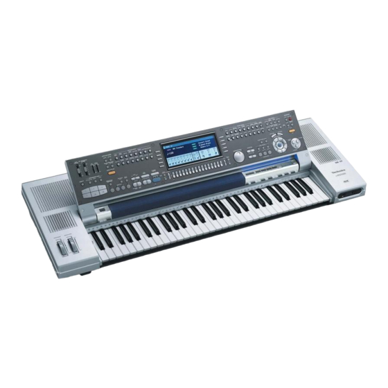
- Page 1 ORDER NO. EMID0207013C0 PCM KEYBOARD SX-KN7000P SX-KN7000PC SX-KN7000EX SX-KN7000EF SX-KN7000EH SX-KN7000EQ SX-KN7000EG SX-KN7000EB SX-KN7000EV SX-KN7000GN SX-KN7000GM SX-KN7000GH SX-KN7000GT SX-KN7000GU (P) U.S.A. (PC) Canada (EX) Norway, Sweden, Denmark, Finland, Spain, Portugal, Greece, Poland, Czech,South Africa (EF) France (EH) Netherlands (EQ) Germany...
-
Page 2: Specifications
(GT) Taiwan (GU) Thailand, Indonesia, Dubai, Brazil, Philippines, Barkley(special) SPECIFICATIONS SPECIFICATIONS 61 KEYS (WITH INITIAL KEYBOARD TOUCH) SOUND GENERATOR 128 NOTES MAX. POLYPHONY... - Page 3 SOUNDS NUMBER OF SOUNDS: 1236 SOUNDS (1187 SOUNDS + 2 ORGAN DRAWBARS + 2 ORGAN TABS + 3 ACCORDION REGISTERS + 41 DRUM KITS) SOUND GROUP: PIANO, GUITAR, STRINGS & VOCAL,BRASS, MALLET & ORCH PERC, WORLD, ORGAN & ACCORDION,SAX & WOODWIND, PAD , SYNTH, BASS, DRUM KITS, DIGITAL...
- Page 4 MAIN VOLUME, APC/ CONTROLS SEQUENCER VOLUME, LINE IN VOLUME, SD VOLUME, BALANCE, MUTE, CONDUCTOR, START/STOP, INTRO & ENDING 1, INTRO & ENDING 2, FILL IN 1, FILL IN 2, COUNT INTRO, SYNCHRO& BREAK,TEMPO/ PROGRAM, TAP TEMPO, FADEIN/OUT, SPLIT POINT PERFORMANCE PADS 20 PRESET BANKS ×...
- Page 5 PLAY, SONG MEDLEY, DISK TOOLS, PREFERENCES, STYLE CONVERT, CUSTOM STYLE LOAD/SAVE LOAD, SAVE, SD CARD FAVORITES SONGS, TECHNICS SONG MEDLEY, SD-AUDIO PLAY, SD-SOUND PLAY, CUSTOM STYLE LOAD/ SAVE, SD CARD TOOLS, SD PREFERENCES PART SETTING, MIXER, SOUND SETTING MASTER TUNING, KEY...
- Page 6 MIC REVERB & EFFECT, REVERB & EFFECT SOUND LOAD OPTION, ALLOCATION, MIXER, SOUND DSP, MULTI, CHORUS, REVERB, EQUALIZER INITIAL, OVERALL CONTROL TOUCH SENSITIVITY, FOOT CONTROLLERS, PANEL MEMORY MODE, MUSIC STYLE ARRANGER MODE, FADE IN/OUT SETTING HOME PAGE SETTING, CUSTOMIZE FAVORITE SETTING, DISPLAY TIME OUT, WALL PAPER SETTING, MIDI SETTING LOAD...
- Page 7 PHONES, FOOT SW 1, 2, TERMINALS FOOT CONTROLLER, EXP PEDAL, MAIN OUT (R /MONO,L), SUB OUT (1,2) AUX IN (R/MONO,L), LINE IN (R/MONO,L), USB, VIDEO OUT, MIDI (IN/ BASS PEDAL, OUT,THRU), MIC 66 W (18 W × 2 FOR MID/ OUTPUT HIGH, 30 W ×...
- Page 8 To prevent the risk of fire, smoke, or electrical shock and to ensure safe operation, please be sure to follow the safety guidelines below. 1. At places where special caution is required, the necessary safety precautions are clearly labeled or printed, for example, on the cabinet, or on the part concerned. Please follow these safety precautions, and also those listed in the Owner'sManual.
-
Page 9: Owners Manual
2.2. Insulation Resistance Test 1. Unplug the power cord and short the prongs of the plug with a jumper wire. 2. Turn on the power switch. 3. Measure the resistance value with an ohmmeter between the jumpered AC plug and each exposed metal cabinet part, such as screw heads, connectors, control shafts, handle brackets, etc. -
Page 10: Midi Implementation Chart
4. MIDI Implementation Chart 5. Keyboard Ranges This keyboard features Touch Response, by which you control the volume by playing the keys harder or softer. 6. Parts Location... -
Page 11: Disassembly Instructions
7. Disassembly Instructions 7.1. Removing the top cabinet 1. Turn the keyboard cabinet upside down, and remove the bottom screws ( pcs.) as shown in Fig.2 2. Place the keyboard bottomside down, and open the top cabinet . Fig.2... - Page 12 The control panel is set up, and remove the top cabinet as shown in Fig.3 Fig.3 7.2. Removing the control panel, power SW panel, SD panel,...
- Page 13 net panel and keyboard unit Remove the top cabinet (see step “Removing the top cabinet ”). Remove the bottom screws( 5pcs.) as shown in Fig.4 Fig.4 Control panel 1. Place the keyboard bottomside down. 2. Remove the control panel holding screws ( 4pcs.) as shown in Fig.7 Power SW panel...
- Page 14 Keyboard unit Remove the keyboard unit holding screws ( 2pcs.) as shown in Fig.7 Fig.5 7.3. Removing the JACK and MAIN printed circuit boards JACK P.C.B. 1. Remove the jack panel mounting screws ( 5pcs.) as shown in Fig.6 2. Remove the JACK P.C.B. mounting screws ( 3 pcs., 3pcs, 3pcs.)as shown in...
- Page 15 MAIN P.C.B. 1. Remove the main shild top case mounting screws ( 6 pcs.) as shown in Fig.7 2. Remove the MAIN P.C.B. mounting screws ( 10pcs.) as shown in Fig.7 Fig.7...
- Page 16 7.4. Removing the FAJ printed circuit board FAJ P.C.B. 1. Remove the FAJ angle mounting screws ( 3pcs.) as shown in Fig.8 2. Remove the FAJ P.C.B. mounting screws ( 6pcs., 3pcs, 9pcs.)as shown in Fig.8 Fig.8...
- Page 17 ASUB P.C.B. disasemble Push the board holder libs as shown in Fig.8 ASUB P.C.B. asemble Paste the tape as shown in Fig.8...
-
Page 18: Pcs.) As Shown In Fig
7.5. Removing the ACP printed circuit board ACP P.C.B. 1. Remove the ACP cover mounting screws ( 3pcs.) as shown in Fig.9 2. Remove the ACP P.C.B.and insuration sheet mounting screw ( pc.) as shown in Fig.9 Fig.9... - Page 19 7.6. Removing the LCD, CPL, CPC, CPR, ROT and INV printed circuit boards Remove the control panel (see step “Removing the control panel, power SW panel, SD panel, net panel and keyboard unit ”). Remove the control panel lid holding screws ( 10pcs.)as shown in Fig.10...
- Page 20 1. Remove the LCD hinge holding screws ( 2pcs.) as shown in Fig.10 2. Remove the LCD holding screws ( 2pcs.) as shown in Fig.10 CPL P.C.B. 1. Pull off the SLIDE VOLUME knob as shown in Fig.10 2. Remove the CPL P.C.B. mounting screws ( 11 pcs.) as shown in Fig.10 CPR P.C.B.
- Page 21 7.7. Removing the SD and SDSW printed circuit boards Remove the SD panel (see step “Removing the control panel, power SW panel, SD panel, net panel and keyboard unit ”). SD P.C.B. Remove the SD P.C.B. mounting screws ( 2pcs.) as shown in Fig.11 SDSW P.C.B.
- Page 22 Remove the SDSW P.C.B. mounting screws ( 3 pcs.) as shown in Fig.11 Fig.11 7.8. Removing the BEND and the HP P.C.B. Remove the top cabinet (see step “Removing the top cabinet ”). BEND P.C.B. Remove the BEND P.C.B. mounting screws ( 2 pcs.) as shown in Fig.12 HP P.C.B.
- Page 23 7.9. Removing the Disk Drive Unit...
- Page 24 1. Remove the Disk Drive unit mounting screws ( 4 pcs. ) as shown in Fig.13 2. Remove the Disk Drive unit holding screws ( 4 pcs. ) as shown in Fig.13 Fig.13 7.10. Removing the Power SW 1. Remove the Power SW panel (see step “Removing the control panel, power SW panel, SD panel, net panel and keyboard unit ”).
- Page 25 2. Remove the power SW mounting screws ( 2pcs. ) as shown in Fig.14 Fig.14 7.11. Removing the 14cm SP, 12cm SP and 6.5cm SP Remove the top cabinet (see step “Removing the top cabinet ”). 14 cm SP Remove the 14 cm SP@holding screws ( 4pcs.) as shown in Fig.15...
- Page 26 12 cm SP Remove the 12 cm SP holding screws ( 4pcs.) as shown in Fig.15 6.5 cm SP Remove the 6.5 cm SP holding screws ( 4pcs.) as shown in Fig.15 Fig.15 7.12. Removing the keys...
- Page 27 Remove the keyboard unit (see step “Removing the control panel, power SW panel, SD panel, net panel and keyboard unit ”). 1. Press downward on the rear of the key as shown in Fig.16 2. While pressing downward on the rear of the key, push the key forward and release it from the chassis.
- Page 28 2. After the service diagnostic screen is displayed on the LCD, release the three keys. (refer to Fig.21 3. Use the corresponding buttons below the “page select” display to select the respective test. Fig.21 8.1. ROM device test Fig.22...
- Page 29 Press the EXECUTE button to begin the test. The test result (OK or NG) is displayed within twenty seconds. If the test result is NG, not only the respective IC, but also a break or short circuit in the ADDRESS/ DATA BUS as well as in any of the strobe signal lines may be the causeof thefailure.
- Page 30 Press the EXECUTE button to begin the test. The test result (OK or NG) is displayed with in a few seconds. If the test result is NG, not only the respective IC, but also a break or short circuit in the ADDRESS/ DATA BUS as well as in any of the strobe signal lines may be thecause of thefailure.
- Page 31 cleaning disk. Then, change the disk used in testing with another disk andreperformthe test. If the trouble is not solved, it is likely that the Disk Drive unit or some other part of the hardware is broken. 8.5. Panel SW & LED test Fig.26 Press all the buttons on the Control Panel and confirm that the corresponding LED lights.
- Page 32 Press the RGBWB, CROSSTALK, SAMPLE, CONTRAST or VIDEO OUT button to begin the respective test. (refer to Fig.27 RGBWB: All the dots light in red, green, blue, white, and finally black. The display can be held by pressing the DISPLAY HOLD button. CROSSTALK: An H pattern is shown.
- Page 33 The operation status of each input action part can be confirmed. If the part is operating properly, “OK” is shown, excluding the Expression Pedal. (refer to Fig.28 When a keyboard key is pressed, the corresponding pitch and velocity aftertouch is displayed (only as long as the key is depressed).
- Page 34 and the MIDI terminal operation is indicated as being OK or NG. (refer to Fig.29 If NG is shown, check both the IN and OUT terminals, as well as the circuit. 8.9. WAVE ROM test Fig.30 Press the EXECUTE button to start the test. The test result (OK or NG) is displayed within thirty seconds.
- Page 35 Fig.32 1. Generate a full amplitude sine wave in the pitch of each key. (No touch, fixed stereo center). If no sound is generated or if the sound is distorted, the sound generator ROM corresponding to the key position is defective. 2.
- Page 36 Load/save test Insert the SD card. Press the START button to begin the test. The test is carried out repeatedly. Data is saved and loaded, and then the two data sets are compared. The number of times that the test results in OK or NG are counted and displayed on the LCD.
- Page 37 Press the EXECUTE button to start the test. The test result (OK or NG) is displayed . If the test result is NG, not only the respective IC, but also a break or short circuit in the ADDRESS/DATA BUS as well as in any of the strobe signal lines may be the causeof the failure.
- Page 38 9.2. Notes on replacing FLASH ROMs The replacement parts include a FLASH ROM with a available memory and the PROGRAM DISKs which contains the program to be written into the PROGRAM ROMs. After replacing the PROGRAM ROM, always write the program into it from the...
- Page 39 PROGRAM DISKs includedinthe replacement parts. For details on programming, see “After replacing the PROGRAM ROM (IC16/IC17) ” . The CUSTOM DATA ROM stores RHYTHM & ACCOMP data for the RHYTHM GROUP/ CUSTOM function. The initial RHYTHM & ACCOMP data is factory-set in the CUSTOM DATA ROM at the time of shipping.
- Page 40 3. Check “Flash Memory Update” is displayed on the LCD, and release the PANEL MEMORY buttons. The program will be written into the FLASH ROM automatically. Replace the floppy disk when instructed. 4. When the operation is complete, “Completed!!” will be displayed on the LCD. 5.
- Page 41 4. When the operation is complete, “Completed!!” will be displayed on the LCD. 5. Turn the power switch off and then back on again. Check the instrument is functioning properly. 10. Measurements and Adjustments ADJUSTMENT EQUIPMENT ADJUSTMENT ADJ. POINT CONNECT METER MEASURING METER TO...
- Page 42 Resistors without symbolic mark are FIXED CARBON FILM RESISTORS (ERD-type). All resistors are 1/4 WATT, ±5 % TOLERANCE unless otherwise designated in schematic diagrams. Table-1 SPECIFICATION SYMBOL Fixed Carbon Film Resistors “FLAME-PROOF” (ERD—F—type) Fixed Wire Wound Resistors “FLAME-PROOF” (ERF—type) Fixed Metal Oxide Film Resistors “FLAME-PROOF”...
- Page 43 SPECIFICATION TYPE SYMBOL Non-Polarized Electrolytic ECEA_KN_type Capacitors Non-Polarized Electrolytic (for ECEA_Y_type Network system) Tantalum Solid Electrolytic ECS_type Capacitors Metalized Plastic Film ECQV_type Capacitors (TF Series) Temperature Compensating ECC_type Ceramic Capacitors High-Dielecytric Constant ECK_type Ceramic Capacitors ECR_type Axial Lead Ceramic ECB_type Capacitors Metalized Polyester Film ECQ_EW_type...
- Page 45 13. SCHEMATIC DIAGRAM...
-
Page 46: Printed Circuit Board
14. Printed Circuit Board 15. Block Diagram 16. Wiring Connection Diagram 17. Replacement Parts List Notes: *Important safety notice: Components identified by mark have special characteristics important for safety. Funrthermore, special parts which have purposes of fire-retardant (resistors), high- quality sound (capacitors),low-noise(resistors), etc. are used. When replacing any of components, be sure to use only manufacture’s specified parts shown in the parts list. - Page 47 *Resistance values are in ohms, unless specified otherwise, 1K=1,000 (OHM), 1M= 1,000K (OHM) *The marking <RTL> indicates that the Retention Time is limited for this item. After the discontinuation of this assembly in production, it will no longer be available. *Since SW consists of buttons and P.C.B.’s, we do not supply it as an individual part (refer to “Manual Keyboard Parts and Control Panel Parts Location...
- Page 48 Ref. No. Part No. Part Name & Description Remarks QGUG1536BA BUTTON A-1 QGUG1536CA BUTTON A-2 QGUG1536EA BUTTON A-4 QGUG1536FA BUTTON A-5 QGUG1537CA BUTTON B QGUG1538BA BUTTON C-1 QGUG1538CA BUTTON C-2 QGUG1539AA BUTTON D QGUG1540BA BUTTON E QGUG1541AA BUTTON F QGUG1542AA BUTTON G QGUG1543BA BUTTON H...
- Page 49 Ref. No. Part No. Part Name & Description Remarks QMFG4076AAK CUSHION QHQG009AA SUSG570A SPRING XYE3+FJ10 SCREW XNS12FZ QMEG011AA THERMISTOR SPRING QWZG010AA THERMISTOR TUBE XTV3+10C SCREW XYE3+FJ10 SCREW XNS12FZ XTW3+10TFZ MIDI JACK SCREW XTB3+10GFZ VIDEO OUT(1) QMFG4107AA CUSHION QMGG029AA FLOATING RUBBER QAUG033AA FDD UNIT QMFG4207AA...
- Page 50 Ref. No. Part No. Part Name & Description Remarks XYE3+FJ10 SCREW QMWG6009BAK 13KEYS RUBBER SWITCH QMWG6010BA 12KEYS RUBBER SWITCH QMFG4176AAK CUSHION QMRG2074AAK HOLDING SHEET QMWG5003CA AFTER TOUCH SENSOR XTW3+10T SCREW SHGG9052A KEY GUIDE RUBBER QMFG1120CA FELT STBG1101B WHITE KEY(C F) STBG1111B WHITE KEY(D) STBG1121B...
- Page 51 Ref. No. Part No. Part Name & Description Remarks QJAG027AB AC CORD EH EV GU GM GT QJAG028AB AC CORD EB GH RJA0035-2X AC CORD QFVG2044A PACKAGED CD-ROM K2DA42E00001 ATTACHMENT PLUG GM GU GT QPGG0522AA CARTON BOX PCB1 SXPG238611 MAIN PCB <RTL>...
- Page 52 Ref. No. Part No. Part Name & Description Remarks ECJ1VB1C104K 0.1U [SPC] C101,02 ECJ1VB1C104K 0.1U [SPC] C108 ECJ1VB1C104K 0.1U [SPC] C110 ECJ1VB1C104K 0.1U [SPC] C111 ECJ1VG1H470J [SPC] C112 ECJ1VG1H100D [SPC] C113 ECJ1VB1C104K 0.1U [SPC] C114-19 ECJ1VG1H470J [SPC] C120,21 ECJ1VG1H100D [SPC] C122 ECJ1VG1H470J [SPC]...
- Page 53 Ref. No. Part No. Part Name & Description Remarks C358 ECJ1VB1H472K 0.0047U [SPC] C359,60 ECJ1VB1C104K 0.1U [SPC] C363 ECJ1VB1C104K 0.1U [SPC] C364,65 ECJ1VG1H681J 680P [SPC] C366,67 ECJ1VG1H102J 0.001U [SPC] C368,69 ECJ1VB1C104K 0.1U [SPC] C370,71 ECJ1VG1H102J 0.001U [SPC] C372-74 ECJ1VB1C104K 0.1U [SPC] C375,76 ECJ1VG1H102J...
- Page 54 Ref. No. Part No. Part Name & Description Remarks CN206 K1KA80A00100 CONNECTOR [SPC] CN207 QJTG02840AA CONNECTOR K1MM40A00002[SPC] CN208,09 K1KA80A00100 CONNECTOR [SPC] CN301 K1KA12A00227 CONNECTOR [SPC] CN302 TJSF34113A CONNECTOR K1KA13A00049[SPC] CN401 K1KA11A00102 CONNECTOR [SPC] CN402 K1KA10A00317 CONNECTOR [SPC] MA2J11100L DIODE [SPC] MA2J11100L DIODE [SPC]...
- Page 55 Ref. No. Part No. Part Name & Description Remarks IC207 C3CBQD000004 [SPC] IC208 C3CBQD000003 [SPC] IC209 C0JBAE000140 2 INPUT OR GATE [SPC] IC301 TC7SH32FUTL C0JBAE000093[SPC] IC302 TC74VHC245F C0JBAZ000505[SPC] IC303 TC74VHC574F C0JBAF000183[SPC] IC304 TC74VHC245F C0JBAZ000505[SPC] IC305 C0JBAZ000874 [SPC] IC306 S21065LKS240 C2HBBY000012[SPC] IC307,08 KM416S1120DT C3ABMG000039[SPC]...
- Page 56 Ref. No. Part No. Part Name & Description Remarks ERJ3GEYJ102V [SPC] ERJ3GEYJ472V 4.7K [SPC] ERJ3GEYJ102V [SPC] R5,R6 ERJ3GEYJ104V 100K D0GB104JA002[SPC] R7-10 ERJ3GEYJ472V 4.7K [SPC] R11,12 ERJ3GEYJ470V [SPC] ERJ3GEYJ472V 4.7K [SPC] ERJ3GEYJ103V D0GB103JA002[SPC] R15-17 ERJ3GEYJ470V [SPC] ERJ3GEYJ103V D0GB103JA002[SPC] R19-21 ERJ3GEYJ472V 4.7K [SPC] ERJ3GEYJ103V D0GB103JA002[SPC]...
- Page 57 Ref. No. Part No. Part Name & Description Remarks R152 ERJ3GEYJ472V 4.7K [SPC] R201 ERJ3GEYJ105V [SPC] R202,03 ERJ3GEYJ470V [SPC] R205-17 ERJ3GEYJ470V [SPC] R218 ERJ3GEY0R00V [SPC] R219-32 ERJ3GEYJ470V [SPC] R234-58 ERJ3GEYJ470V [SPC] R301,02 ERJ3GEYJ472V 4.7K [SPC] R303 ERJ3GEYJ101V [SPC] R304 ERJ3GEYJ103V D0GB103JA002[SPC] R305,06 ERJ3GEYJ333V...
- Page 58 Ref. No. Part No. Part Name & Description Remarks R427 ERJ3GEYJ394V 390K [SPC] R428 ERJ3GEYJ220V [SPC] R429 ERJ3GEYJ101V [SPC] R430-32 ERJ3GEYJ472V 4.7K [SPC] R433 ERJ3GEYJ101V [SPC] R434-37 ERJ3GEY0R00V [SPC] R438 ERJ3GEYJ102V [SPC] R439 ERJ3GEYJ472V 4.7K [SPC] R440,41 ERJ3GEYJ682V 6.8K D0GB682JA002[SPC] R442 ERJ3GEYJ103V D0GB103JA002[SPC]...
- Page 59 Ref. No. Part No. Part Name & Description Remarks Z208-10 EXBV8V470JV 47 X 4 [SPC] Z211 EXBV8V101JV 100 X 4 [SPC] Z212-46 EXBV8V470JV 47 X 4 [SPC] Z301-03 EXBV8V101JV 100 X 4 [SPC] Z304-07 EXBV8V221JV 220 X 4 [SPC] Z308 EXBV8V472JV 4.7K X 4 [SPC]...
- Page 60 Ref. No. Part No. Part Name & Description Remarks C546,47 F1D1H101A012 100P C548,49 ECEA1CKN100B 16V 10U C550-53 ECQB1H223JF3 0.022U C554,55 QCBG1H473ZFA 0.047U F1E1H473A001 C556,57 F1D1H470A006 C558,59 QCBG1H473ZFA 0.047U F1E1H473A001 C560,61 ECEA1CKN100B 16V 10U C562,63 ECBT1H150JC5 C564 ECBT1H220JC5 C565,66 QCBG1H473ZFA 0.047U F1E1H473A001 C567 ECBT1H220JC5...
- Page 61 Ref. No. Part No. Part Name & Description Remarks CN508 SJPG1320A CONNECTOR CN641 SJPG7JS030A CONNECTOR D501-07 RVD1SS133TA DIODE B0AACK000004 D509 10 AK03WK DIODE B0JAMD000005 D511 MA4150-M DIODE MAZ41500M D512 RVD1SS133TA DIODE B0AACK000004 D641 MA4082-MTA DIODE MAZ40820MF D642 MA4033M DIODE MAZ40330M D643 MAZ40560MF DIODE...
- Page 62 Q643 2SA1643LF645 TRANSISTOR B1BCED000002...
- Page 63 Ref. No. Part No. Part Name & Description Remarks Q644 2SC1815TPE2 TRANSISTOR B1AACF000023 Q645,46 2SA1015TPE2 TRANSISTOR B1ACCF000016 Q647,48 2SC1815TPE2 TRANSISTOR B1AACF000023 R501 ERDS2FJ472 4.7K R502 ERDS2FJ104 100K R503,04 ERDS2FJ222 2.2K R505 ERDS2FJ104 100K R506 ERDS2FJ152 1.5K R507 ERDS2FJ103 R508 ERDS2FJ683 R509 ERDS2FJ222 2.2K...
- Page 64 Ref. No. Part No. Part Name & Description Remarks R590-92 ERDS2FJ102 R593,94 ERDS2TJ183 R595 ERDS2TJ682T 6.8K R596,97 ERDS2FJ103 R598,99 ERDS2FJ563 R600 ERDS2FJ332 3.3K R601,02 ERDS2FJ473 R603 ERDS2TJ272T 2.7K R604,05 ERDS2FJ473 R606 ERDS2FJ332 3.3K R607,08 ERDS2FJ222 2.2K R609 ERDS2FJ473 R610 ERDS2TJ105T R611 ERDS2FJ473 R612,13...
- Page 65 R671-73 ERDS2FJ101...
- Page 66 Ref. No. Part No. Part Name & Description Remarks R674 ERDS2FJ473 R675,76 ERDS2FJ103 R677 ERDS2TJ105T R678 ERDS2FJ102 R679 ERTD2ZHK153T R680 ERDS2FJ273 R681-83 ERDS2FJ102 <JACK P.C.B.> PCB7 SXPG238711B JACK PCB <RTL> C701,02 QCBG1H473ZFA 0.047U F1E1H473A001 C705-07 QCBG1H473ZFA 0.047U F1E1H473A001 C709-16 QCBG1H473ZFA 0.047U F1E1H473A001 CN701...
- Page 67 Ref. No. Part No. Part Name & Description Remarks <INV P.C.B.> PCB8 SXPG238811B INV PCB <RTL> C801 ECUV1C104KBV 0.1U ECJ1VB1C104K C802 ECEA1AKS221 6V 220U C803 ECQV1H104JZ 0.1U C804 ECCW3F180JGE C805 ECUV1C104KBV 0.1U ECJ1VB1C104K CN801 K1MN20B00049 CONNECTOR CN802 SJPG1JS140A CONNECTOR CN803 RJP4G27ZA CONNECTOR K1KA04A00063...
- Page 68 Ref. No. Part No. Part Name & Description Remarks Q839,40 2SB0709ARL TRANSISTOR Q841,42 2SD0601AQL TRANSISTOR Q843 2SB0709ARL TRANSISTOR Q844 2SD0601AQL TRANSISTOR Q845 2SB0709ARL TRANSISTOR Q846 2SD0601AQL TRANSISTOR Q847,48 2SB0709ARL TRANSISTOR Q849 2SD0601AQL TRANSISTOR Q850-52 2SB0709ARL TRANSISTOR Q853,54 2SD0601AQL TRANSISTOR Q855 2SB0709ARL TRANSISTOR Q856...
- Page 69 Ref. No. Part No. Part Name & Description Remarks PCB5 SXPG232941 ACP PCB <RTL>EF EH EV GN GH PCB5 SXPG232951 ACP PCB <RTL>P PC PCB5 SXPG232961 ACP PCB <RTL>GM GU GT F1B2E4720001 4700P ECQU2A104MN XBA1C20NB100 FUSE 2A (P PC) XBA2C12TB0L FUSE T1.25A (GU GT GM) XBA2C08TB0L...
- Page 70 D1110 LN382GPXVTX3 LNJ382GKGX02...
- Page 71 Ref. No. Part No. Part Name & Description Remarks D1111 LN382GPXVTX3 LNJ382GKGX02 D1112 LN382GPXVTX3 LNJ382GKGX02 D1113 LN282RPXVTX3 LNJ282RKRX02 D1114 LN282RPXVTX3 LNJ282RKRX02 D1115 LN282RPXVTX3 LNJ282RKRX02 D1116 LN282RPXVTX3 LNJ282RKRX02 D1117 RVD1SS133TA DIODE B0AACK000004 D1118 RVD1SS133TA DIODE B0AACK000004 D1119 RVD1SS133TA DIODE B0AACK000004 D1120 RVD1SS133TA DIODE B0AACK000004...
- Page 72 Ref. No. Part No. Part Name & Description Remarks X1101 EFOEC4004T3 4MHZ CERAMIC OSCILATOR <CPC P.C.B.> PCB12 SXPG238911B CPC PCB <RTL> CN1107 K1KA12C00012 CONNECTOR CN1108 K1KA06C00008 CONNECTOR D1195-02 RVD1SS133TA DIODE B0AACK000004 D1203-06 LN282RPXVTX3 LNJ282RKRX02 D1207-38 RVD1SS133TA DIODE B0AACK000004 SW1155-94 EVQ21405R PUSH SWITCH EVQ21405RJ <CPR P.C.B.>...
- Page 73 Ref. No. Part No. Part Name & Description Remarks D1102 RVD1SS133TA DIODE B0AACK000004 D1103 RVD1SS133TA DIODE B0AACK000004 D1104 RVD1SS133TA DIODE B0AACK000004 D1105 RVD1SS133TA DIODE B0AACK000004 D1106 RVD1SS133TA DIODE B0AACK000004 D1107 LN282RPXVTX3 LNJ282RKRX02 D1108 B3ABA0000397 DIODE D1109 LN282RPXVTX3 LNJ282RKRX02 D1110 LN382GPXVTX3 LNJ382GKGX02 D1111 LN282RPXVTX3...
- Page 74 Ref. No. Part No. Part Name & Description Remarks R928 ERJ3GEYJ220V R929-31 ERJ3GEYJ101V SW921 JSE0013 SWITCH K0L1BA000007 <SDSW P.C.B.> PCB17 SXPG239011C SDSW PCB <RTL> CN901 SJPG2JS100A CONNECTOR D901 LN282RPXVTX3 LNJ282RKRX02 D902 LN382GPXVTX3 LNJ382GKGX02 D903 LMW9A8BYB0A1 DIODE Q901,02 2SC1815TPE2 TRANSISTOR B1AACF000023 R901-03 ERDS2FJ102 R904,05...
- Page 75 Ref. No. Part No. Part Name & Description Remarks QCBG1H104ZFA 50V 0.1 F1E1H104A001 TCBT1H151KB5 150P F1D1H151A012 TCBT1H151KB5 150P F1D1H151A012 TCBT1H151KB5 150P F1D1H151A012 TCBT1H151KB5 150P F1D1H151A012 TCBT1H151KB5 150P F1D1H151A012 TCBT1H151KB5 150P F1D1H151A012 TCBT1H151KB5 150P F1D1H151A012 TCBT1H151KB5 150P F1D1H151A012 D49-96 RVD1SS133TA DIODE B0AACK000004 HD74LS138P C0JACN000001...
- Page 76 Ref. No. Part No. Part Name & Description Remarks QEXGVH03025B WIRE WITH CONNECTOR QEXGSS08040A WIRE W/CON(CPR -MAIN) QEXGSS13050A CONNECTION WITH WIRE QEXGSS14055A CONNECTOR WIRE QEXGZA04010A WIRE W/CON(CPL -INV) QEXGZA04105A WIRE W/CON(CPL -BEND) QEXGZA06010A WIRE W/CON(CPL -CPC) QEXGZA07055A WIRE W/CON(CPL -CPR) QEXGZA12015A WIRE W/CON(CPL -CPC) QEXGZA13041A...
- Page 77 REF.NO. DESCRIPTION 40(G) SOUND GROUP(DIGITAL DRAWBER,ORGAN TABS,ACCORDION REGISTER,PAD) 40(H) SOUND GROUP(SYNTH,BASS,DRUM KITS,MEMORY) 41(A) FADE IN/OUT 41(B) TRANSPOSE 41(C) R1/R2 OCTAVE 42(A) MUSIC STYLIST 42(B) SD LOAD 43(A) OTHER PART&FR,HELP 43(B) DISPLAY HOLD 45(A) CONTRAST,MUTE 45(B) PAGE FILL IN,INTRO&ENDING TAP TEMPO,SYNCHRO&BREAK TECHNI-CHORD,SOLO CONDUCTOR(LEFT,RIGHT2,RIGHT1) 51(A)
- Page 78 S020700000 HM/AM 2002 Matsushita Electric Industrial Co., Ltd. All rights reserved. Unauthorized copying and distribution is a violation of law.
- Page 79 TONE SIGNAL CONTROL SIGNAL JACK CN701 CN105 CN702 FLOPPY LCD BACK DISC LIGHT JK702 Q701 DRIVE MIDI THRU JK703 MIDI OUT JK704 IC701 CN801 CN804 PHOTO MIDI IN COUPLER T801 SW701 BASSPEDAL TRANSFORMER Q102 Q801,802 JK706 JK707 CN802 CN803 Q105,106 FOOT JK708 MIDI RX...
- Page 80 SD I/F IC402 USB+ USB- CN401 CN921 CN922 SDDAT0-SDDAT3 SD DECORDER MIDI RX IC407 IC410 IC414 USB CPU SDA1-SDA16 SDD0-SDD15 USBM.TX SDIU SDA1-SDA18 CONVERTER FLASH SDD0-SDD15 IC406 IC409 DU0-DU7 DATA BUS DU0-DU7 SDOU CONVERTER IC403 IC401 SDA1-SDA18 SDD0-SDD15 USB.SI USB.SO EEPROM SD u-COM IC408...
- Page 81 IC1101 CN1185 CN1107 IC1001 SW0-7 SWITCHES & CN1003 SWITCHES Q1101- & SW0-7 IC1102 1108 CN1106 CN1108 Q1002- 1007 CM0-2 DECORDER DRIVE TO MAIN SWITCHES CN103 & CM0-5 DRIVE 8 BIT 8 BIT MICROCOMPUTER MICROCOMPUTER CN1001 CN1101 SIN,SOUT SIN,SOUT CLK,CNTR1 CLK,CNTR1 SEG6-7 IC1002, CN1104...
- Page 82 IC644 FP641 FP642 D646-D649 CN641 +15V +15A REGULATOR POWER POWER IC641, IC641, TRANSFORMER SWITCH Q643,644 Q641,642 Q645-648 IC643 FP643 +3.3V OVERCURRENT -15V +3.3D -15A REGULATOR REGULATOR PROTECTOR REGULATOR CORD CN502 D644,645 TO MAIN CN301 IC507 CN501 JK506 SUBOUT L JK507 SUBOUT R TO MAIN JK501...
- Page 83 MAIN P.C.B. (COMPONENT SIDE) MAIN P.C.B. (FOIL SIDE) R152 IC105 R132 R136 R133 D102 R134 C128 D101 C126 Q102 Q103 CN103 C123 Q101 R125 C124 R127 C139 R128 C122 C119 C140 C141 R148 C118 R131 C117 R139 R130 C116 R129 R150 C158 C115...
- Page 84 FAJ P.C.B. ASUB P.C.B. (COMPONENT SIDE) ASUB P.C.B. (FOIL SIDE) SUMR SUML Q826 R835 CN821 CN820 R823 R822 R821 R820 R831 CN503 R868 C506 R869 C611 MAIN OUT L C590 C823 C612 R827 C829 R640 Q860 R871 R846 J627 J626 R859 C616 R639...
- Page 85 CPL P.C.B. MAIN RHYTHM GROUP VOLUME AUTO PLAY CHORD D1178 APC / SEQUENCER D1148 D1146 D1144 D1142 D1132 D1130 D1128 D1126 D1176 D1174 J1240 J1249 LINE IN J1239 8 & 16 BEAT ROCK & POP BALLAD BALLROOM MOVIE & SHOW ENTERTAINER ORGANIST J1234...
- Page 86 CPR P.C.B. SOUND GROUP SEQUENCER J1026 D1056 D1014 D1122 D1116 D1095 D1067 D1053 D1039 D1025 D1011 D1070 D1042 D1028 D1081 D1074 D1109 D1060 Q1004 D1046 D1103 J1003 SAX & WOODWIND ORGAN & ACCORDION DIGITAL EFFECT VARIATION PLAY EAST REC GUITAR STRINGS &...
- Page 87 JACK P.C.B. FOOT CONTROLLER BASS PEDAL MIDI IN MIDI IN / BASS PEDAL MIDI OUT MIDI THTU VIDEO OUT (Example) FOOT SW 1 FOOT SW 2 EXP PEDAL SW701 CN702 Transistor's symbolmark: JK707 JK708 JK701 JK709 JK704 JK703 JK702 J607 C702 D707 JK706...
- Page 88 MKB2 P.C.B. C#26 D#28 F#31 G#33 A#35 C#38 D#40 F#43 G#45 A#47 (SXPG232421B) MKB3 P.C.B. HP P.C.B. CN751 C754 (Example) JK751 Transistor's symbolmark: L751 HEAD PHONE C#50 D#52 F#55 G#57 A#59 E C B CN10 AFTER TOUCH D105 Applied for all transistors SENSOR ADJ D108 D109...
- Page 89 Keyboard [ SX-KN7000 ] Function Transmitted Recognized Remarks Default 1 - 1 6 1 - 1 6 Assigned to the part. Basic Channel Changed 1 - 1 6 1 - 1 6 Default OMNI OFF , POLY MODE M o d e 3 Messages M=1 only Mode...
- Page 90 MUSIC STYLIST You can choose to have all the settings of this instrument automatically set. AUTO PLAY CHORD Add an automatic RHYTHM GROUP accompaniment to your Various rhythm patterns are selected rhythm. available for each rhythm group. RHYTHM GROUP MAIN APC/SEQUENCER AUTO PLAY CHORD VOLUME...
- Page 91 DISPLAY TECHNI-CHORD Displays performance information, function settings Block chords are and other messages. automatically added to the • Adjust the readability with the CONTRAST melody. buttons at the lower left side of the display. SEQUENCER SOUND GROUP Record and play back your Various sounds are available for each performance.
- Page 92 This Keyboard has many settable functions and storable memories. However, you can return the settings and memory to the factory-preset status. Press the PROGRAM MENUS button to turn Press the OK button. it on. The display changes to the confirmation dis- play.
- Page 93 If you wish to retain the settings and stored memory contents for recall at a later time, store the desired data on a disk/SD card. The backup memory does not function for the stored contents until the power has been on for about 10 minutes. Data from previous Technics models may be limited to PERFORMANCE data. SZ-FC2 SZ-E2 SZ-P1...
- Page 94 (Left side) VIDEO OUT MIDI The display images or lyrics when playing songs, These terminals are for connection to another and the image of the display are output through MIDI instrument. this terminal. output mode (NTSC/PAL) MIDI IN/BASS PEDAL selected. Set this switch to BASS PEDAL to connect a commercially available MIDI pedal unit.
- Page 95 (Right side) AUX IN A microphone can be connected to this terminal. This terminal receives input signals from an ex- ternal instrument. To receive a monaural signal, connect to the R/MONO terminal. LINE IN The input signal volume is not affected by the This terminal receives input signals from an ex- instrument’s MAIN VOLUME setting.
- Page 96 The following changes in performance may occur in the Technics Keyboard but do not indicate trouble. Phenomenon Remedy The buttons, keys, etc. malfunction. Turn off the POWER button once, then turn it on again. If this procedure is not successful, turn off the POWER button once.
- Page 97 Phenomenon Remedy Storage is not possible. The remaining memory capacity of the COMPOSER is 0. Setting the time signature is not possible. The time signature cannot be changed for a pattern which is currently recorded in the COMPOSER. If you wish to change the time signature, first follow the procedure to clear the memory.
- Page 98 Contents Contents The data on the disk that you are using It is only possible to merge melody is for a different product. tracks. Tracks such as rhythm, chord and An error has occurred while the disk was control cannot be merged. loading.
- Page 99 Contents Special tracks such as CHORD (APC), RHY and CTL exist in the song from which copying incompatible with the destination song because it is in the GM mode. AUTO PUNCH recording has been unsuccessful because SEQUENCER operation was interrupted before the PUNCH OUT measure was reached.
- Page 100 SCHEMATIC DIAGRAM-1 MAIN 1/5 CIRCUIT IORST A(0-25) D(0-31) +3.3D R1 100 SELE.LED R22 10K FDC.TC PMUT SD.CS R24 10K 4.7K 2SB709ARTX USB.SD 100K USB.ST USB.MAITU 2SD601AQTX MIDI.TX DSP.RST 0.22 MIDI.RX 11.2096M CP.CLK 4.7K CP.DATA +3.3D +3.3D MN103002A (32bit MICRO-CONTROLLER) C8 0.1 Z8 4.7Kx4 Z13 4.7Kx4 A(0)
- Page 101 +3.3D +3.3D +3.3D +3.3D Z15 4.7Kx4 Z21 4.7Kx4 D(0) D(16) C28 0.1 C29 0.1 D(1) D(17) D(2) D(18) D(3) D(19) RESET Z17 4.7Kx4 Z22 4.7Kx4 D(4) D(20) D(5) D(21) TC7W08FU TC7W08FU D(6) D(22) D(7) D(23) TC7W08FU TC74VHC08F Z19 4.7Kx4 Z23 4.7Kx4 D(8) D(24) +3.3D...
- Page 102 SCHEMATIC DIAGRAM-2 +3.3D +3.3D +3.3D +3.3D C32 0.1 C34 0.1 C36 0.1 C38 0.1 JP7 0 VCC VCC BYTE VCC VCC BYTE LCAS RESET A(21) BCAS RY/BY A(22) A(20) JP12 A(21) A(19) A(20) A(18) A(19) A(17) D(31) A(17) D(31) A(18) D(31) A(16) D(31)
- Page 103 +3.3D +3.3D +3.3D C38 0.1 C41 0.1 C41 0.1 BYTE BYTE BYTE RESET RESET RY/BY RY/BY A(21) A(21) A(20) A(20) CE 26 CE 26 JP12 A(19) A(19) OE 28 OE 28 A(18) A(18) WE 11 WE 11 A(17) A(17) D(31) A(16) D(31) A(16)
- Page 104 SCHEMATIC DIAGRAM-3 MAIN 2/5 CIRCUIT +3.3D R106 IC102 R113 TC7WU04FUTL R108 1M X105 IC101 CN101 Z103 1Kx4 C102 H1A5005B0014 C0JBAB000164 +3.3D IC101 IC102 C0JBAB000164 TC7WU04FUTL R110 1M Z101 47x4 50MHz R109 SIDE R112 X102 WPRT H0J177500018 TRKO X103 H0J240500016 C120 C127 C101 C112...
- Page 105 R113 +3.3D C136 24 23 22 21 20 19 18 17 16 15 14 13 Z107 100x4 MEDIA IO0 D(23) MEDIA IO1 D(22) WDATA D(21) WGATE D(20) HDSEL C137 Z108 100x4 STEP C125 D(19) D(18) D(17) MTRI/IOLE D(16) DSI/PD MTRO DACK R123 C138...
- Page 106 SCHEMATIC DIAGRAM-4 LCD.WAIT FDC DRQ Q103 FDC TC UN511NTX +3.3D FDC INT FDC DACK R152 FDC CS 4.7K 4.7K TDS.SNS CR.DATA C143 Q104 R137 R138 CR.CLK UN5216 4.7K 4.7K 4.7K CN103 3.3D C142 DATA +3.3D R133 C145 +3.3D Q102 R136 R135 R132 7 EXP...
- Page 107 2/2)
- Page 108 SCHEMATIC DIAGRAM-5 MAIN 3/5 CIRCUIT CKOUT LRCK SD00 SD01 MIC.SNS DSP.FLAGB LORST DSP.RST DAC.MDI IC306 DAC.MC S21065LKS240 DAC.ML (DIGITAL SIGNAL PROCESSOR) MTMG +3.3D LRCKX BCKX SDOE(0-3) SDIE(0-3) +3.3D C301 C306 RFSS R301 4.7K RLKB SDOE(0) DRBA SDOE(1) DRBB D(23) DD(7) D(16-31) TFSS D(22)
- Page 109 +3.3D Z308 4.7Kx4 C324 0.1 DA(8) DA(9) C325 0.1 DA(10) DA(11) C326 0.1 Z313 4.7Kx4 DA(12) DA(13) DA(14) DA(15) LDQM MDQM Z317 4.7Kx4 DA(16) DD(31) C319 DA(17) DD(30) DA(18) DD(29) DA(19) DD(28) DA(13) DD(27) DD(26) BSEL Z318 4.7Kx4 DA(9) DD(25) DA(20) DA(8) DD(24)
- Page 110 SCHEMATIC DIAGRAM-6 R323 680 R337 6.8K C380 220P C370 0.001 R354 C304 R328 R334 6V100 Q303 6.8K 6.8K 2SD601AQTX C305 D306 IC314 16V10 MA8039HTX C363 IC315 M5218AFPE3 C376 M5218AFPE3 (OP.AMP) 0.001 (OP.AMP) IC314 IC311 M5218AFPE3 C0FBBK000025 (OP.AMP) R329 R335 (D/A CONVERTER) 6.8K 6.8K R304 10K...
- Page 111 CN301 K1KA12A00227 +15A +15A +15A R338 10K C382 150P C348 0.1 C368 0.1 C373 0.1 +3.3D +3.3D R339 10K +3.3D R347 47K FAJ 1/2 IC312 IC313 IC314 M5218AFPE3 M5218AFPE3 M5218AFPE3 CIRCUIT (CN502) ON (OP.AMP) (OP.AMP) (OP.AMP) SCHEMATIC DIAGRAM-11 R341 15K 33BA.GC +3.3BA 33BB.GC...
- Page 112 SCHEMATIC DIAGRAM-7 MAIN 4/5 CIRCUIT SDIE(0-3) SDOE(0) SDOE(0-3) SDOE(1) SDOE(2) SDOE(3) BCKX Z211 100x4 +3.3D +3.3D Z206 4.7Kx4 D201-D208 MA111-TX KS(0) D201 KS(1) D202 KS(2) D203 KS(3) D204 IC209 Z207 4.7Kx4 KF(0) D205 +3.3D T7SZ32FUT85L KF(1) D206 KF(2) D207 KF(3) D208 CN201 R207...
- Page 113 R225 AWAY(0) +3.3D C227 R226 AWAY(1) Z219 47x4 AWAY(20) Z217 47x4 AWAY(2) AWAY(21) AWAY(3) AWAY(19) AWAY(4) AWAY(8) IC201 BYTE AWAY(5) R221 AWAY(22) C1BB00000709 AWAY(9) AWAY(21) MASTER TONE AWAY(6) AWAY(10) GENERATOR LSI AWAY(20) AWAY(7) AWAY(11) AWAY(19) AWAY(17) AWAY(12) +3.3D AWAY(18) AWAY(18) Z220 47x4 AWAY(17) Z221 47x4...
- Page 114 SCHEMATIC DIAGRAM-8 IC205 R246 C1BB00000709 SUB TONE GENERATOR LSI +3.3D +3.3D R248 SD03 WCEV1 R249 CKOUT WCEV0 SDSUB0 WAY0 WAY1 SDSUB1 SDSUB2 WAY2 SDSUB3 WAY3 BCKSUB WAY4 LRCKSUB WAY5 C231 C242 WAY6 WAY7 WAY17 WAY18 C243 AVDD4 WAY20 WAY21 WAY19 WAY8 WAY9 WAY10...
- Page 115 CN202 CN205 QJTG02840AA QJTG02840AA A(19) A(19) A(18) A(18) A(17) A(17) A(16) A(16) A(15) A(15) R250 BWAY(0) A(14) A(14) R251 BWAY(1) A(13) A(13) Z238 47x4 BWAY(20) A(12) A(12) Z236 47x4 BWAY(2) BWAY(21) A(11) A(11) BWAY(3) BWAY(19) A(10) A(10) BWAY(4) BWAY(8) A(9) A(9) BWAY(5) +3.3D...
- Page 116 SCHEMATIC DIAGRAM-9 MAIN 5/5 CIRCUIT SDCS +5DV C419 C476 0.22 SD PON SDDATA-ST MHDK P68/WAIT/SBT2 MHRE RE/P61 PULLUP MHWEL WEL/P62 PULLUP MHWEH WE/_WEH/P63 P75/SBO1 P50/_CS0/TM130A P74/SBI1 FM MCS P51/_CS1/TM130B P73/SBT1/DMUX SYSCKRST P52/_CS2/TM140A P72/SBO0/UCAS MHCS P53/_CS3/TM140B P71/SBIO0/LCAS/CAS +3.3D XNPO P54/_BREQ P70/SBT0/RAS P55__BRACK C407 0.1 C424...
- Page 117 R424 100K R425 100K C419 R463 R414 R415 Q401 2SD601AQTX SDDATA-ST C409 16V10 100 99 98 97 96 95 94 93 92 91 90 89 88 87 86 85 84 83 82 81 80 79 78 77 76 SDD(7) HD07 C410 0.1 VDD2 SYCK0...
- Page 118 SCHEMATIC DIAGRAM-10 51 52 53 54 55 56 57 58 59 60 61 62 63 64 65 66 67 68 69 70 71 72 73 74 75 76 77 78 79 80 R430 P44/C50 4.7K P51/WRH/BHE P53/BCLK R431 P54/HLDA P107/AN7/KI3 4.7K P106/AN6/KI2 IC407...
- Page 119 USBM.TX MIDI.RX USB.WAITM USB.WAITH USB.SI USB.SO DAC MDI 41 42 43 44 45 46 47 48 49 50 51 52 53 54 55 56 57 58 59 60 61 62 63 64 R450 P30/RST P74/OBF1 P73/IBF1/WLDA P33/DMAOUT P71//HOLD P34/XAOUT R447 33 P35/STNCOUT USB+ R448 33...
- Page 120 SCHEMATIC DIAGRAM-11 FAJ 1/2 CIRCUIT +15A LINE IN C509 0.047 R / MONO IC501 NJM4558L JK502 JK503 JK504 (OP.AMP) QJJG019AA QJJG019AA QJJG019AA JK501 QJJG010AA C510 0.047 -15A L501 QLQGT3T131LA L502 QLQGT3T131LA C503 0.0047 C507 0.047 CN502 R502 100K SJPG1JS120A C518 0.0047 C523 0.0047 C534 0.0047 C540 0.00...
- Page 121 +15M +15A +15M AUX IN SUB OUT C568 0.047 C558 0.047 R / MONO IC507 IC506 IC509 NJM4558L NJM4558L NJM4558L JK504 JK505 JK506 JK507 (OP.AMP) (OP.AMP) (HEADPHONE AMP) QJJG019AA QJJG019AA QJJG019AA QJJG019AA C569 0.047 C559 0.047 C556 47P -15A -15A -15A L504 QLQGT3T131LA...
- Page 122 SCHEMATIC DIAGRAM-12 +15A Q514 B1ACCF000016 +15M +15PM MAIN OUT C592 0.047 D510 R633 AK03WK R / MONO 4.7K IC511 NJM4558L JK508 JK509 D512 (OP.AMP) QJJG019AA QJJG019AA RVD1SS133TA D511 MA4150MTA +VCCF C593 0.047 R637 3.3K C585 47P -15A L509 PMUT QLQGT3T131LA R604 47K R636 R598...
- Page 123 CN504 SJPG1JS050A L508 QLBG005A R588 1W68 L505 QLBG005A R589 1W68 L506 QLBG005A L507 QLBG005A Q508 B1MADFC00001 C582 C581 0.0047 0.0047 -VCC +VCC CN507 L512 C605 SJPG1300A QLQGT1D600LA R601 47K R614 47K R680 SPL+ R621 R626 C584 C602 SPL- R627 FP501 R679 K5G202AA0003 CN508...
- Page 124 SCHEMATIC DIAGRAM-13 ACP CIRCUIT POWER VOLTAGE POWER TRANSFORMER PRODUCTS FOR GU GT SELECTOR BLUE 4700P BLACK AC IN 10UHX2 100V0.1 BLUE AC POWER CORD POWER TRANSFORMER PRODUCTS FOR BLUE 4700P BLACK AC IN 10UHX2 100V0.1 BLUE POWER TRANSFORMER PRODUCTS FOR OTHERS BLUE 4700P BLACK...
- Page 125 FAJ 2/2 CIRCUIT L647 L649 +VCCF QLBG005A QLBG005A +VCC IC644 C0CAALG00016 R667 CN641 FP642 L643 D646 (+15V REGULATOR) SJPG7JS030A K5G402AA0003 QLBG005A SVDGS3V20-15 1/4W +15A D647 C645 C656 D658 C641 C652 C654 C661 C664 SVDGS3V20-15 10V0.1 25V4700 25V4700 0.047 B0JAMD000005 0.047 0.047 16V100 L644...
- Page 126 SCHEMATIC DIAGRAM-14 ASUB CIRCUIT MUTE +15A CN820 QJUG05309AA R833 R838 R835 R841 C827 4.7K 150P G-R2 1/4W 1/4W G-L2 Q824 Q828 Q833 2SB0709ARL 2SB0709ARL 2SD0601AQL AE 5 G-R1 3 RIN 2 G-L1 Q826 Q827 2SB0709ARL 2SB0709ARL D820 R844 MA111TX 4.7K C823 470P R845...
- Page 127 MUTE +VCC +15A +VCC R861 R857 C827 C829 R859 R863 C837 150P 4.7K 150P 25V47 1/4W 1/4W Q848 Q852 Q833 Q836 Q854 Q856 2SB0709ARL SD0601AQL 2SD0601AQL 2SB0709ARL 2SD0601AQL 2SD0601AQL GATE-L1 GATE-R1 Q850 Q851 Q837 Q857 2SB0709ARL 2SB0709ARL 2SB0709ARL 2SB0709ARL D824 R850 R867 R844...
- Page 128 SCHEMATIC DIAGRAM-15 CPL CIRCUIT VR1104 +3.3D CN1104 D2B4A14B0003 SEG0 VOLUME SJPG2JS130A MICVOLIN MICVOLOUT SW1102 D1101 D1117 IC1101 B0AACK000004 EVQ21405R B0AACK0000 C2BBDB000023 L/VIN-L (8BIT MICROCOMPUTER) L/VIN-R +3.3D LCDL 4 L/VOUT-L LINE IN VR1105 L/VOUT-R VOLUME D2B4C53A0002 D1102 SW1103 D1118 SUMR B0AACK000004 EVQ21405R B0AACK0000 SUML...
- Page 129 SEG1 SEG2 SEG3 SEG4 SEG6 SEG7 SW1102 SW1110 SW1118 SW1126 SW1134 SW1142 SW1150 D1117 D1133 D1149 D1165 D1181 D1190 EVQ21405R B0AACK000004 EVQ21405R B0AACK000004 EVQ21405R B0AACK000004 EVQ21405R B0AACK000004 EVQ21405R B0AACK000004 EVQ21507K B0AACK000004 EVQ21405R MEMORY/LOAD MOVIE SHOW INTRO & ENDING 1 VARIATION & WSA 3 PAD 5/SOLO MUSIC STYLIST SW1103...
- Page 130 SCHEMATIC DIAGRAM-16 CPC CIRCUIT SEG5 SEG8 SEG9 SEG10 SEG11 D1195 SW1155 D1207 SW1163 D1215 SW1171 D1223 SW1179 D1231 SW1187 B0AACK000004 EVQ21405R B0AACK000004 EVQ21405R B0AACK000004 EVQ21405R B0AACK000004 EVQ21405R B0AACK000004 EVQ21405R OTHER PARTS/TG MUTE UP 3 MUTE UP 7 MUTE UP 11 MUTE UP 15 D1196 SW1156...
- Page 132 SCHEMATIC DIAGRAM-17 CPR CIRCUIT IC1001 C2BBDB000023 (8BIT MICROCOMPUTER) +3.3D +3.3D SEG0 SEG1 SEG2 D1001 SW1001 D1015 SW1009 D1029 SW1017 RVD1SS133TA EVQ21405R RVD1SS133TA EVQ21405R RVD1SS133TA EVQ214 C1010 0.047 +3.3D TECHOI-CORD SOLO PART SELECT LEFT CN1001 K1KA07C0007 X1001 D1002 SW1002 D1016 SW1010 D1030 SW1018 EF0EC4004T3...
- Page 133 SEG2 SEG3 SEG4 SEG5 SEG6 SEG7 SEG8 SEG9 D1029 SW1017 D1043 SW1025 D1057 SW1033 D1071 SW1041 D1085 SW1049 D1099 SW1057 RVD1SS133TA EVQ21405R RVD1SS133TA EVQ21405R RVD1SS133TA EVQ21405R RVD1SS133TA EVQ21405R RVD1SS133TA EVQ21405R RVD1SS133TA EVQ21405R PART SELECT LEFT TRANSPOSE R1 (+) TRANSPOSE R1 (-) LCDR 5 LCDR 4 LCDR 3...
- Page 134 SCHEMATIC DIAGRAM-18 JACK CIRCUIT CN702 C702 K1FB104B0023 0.047 MIDI THRU IN / BASS PEDAL L703 QLQGT3T131LA JK702 JK703 JK704 MIDI IN QJJG020AA QJJG020AA QJJG020AA SW701 K0D112B00112 JK701 K4BK01H00001 VIDEO L704 L705 L706 QLQGT3T131LA QLQGT3T131LA QLQGT3T131LA L701 QLQGT3T131LA R703 R706 R707 IC701 C705 PC900V...
- Page 135 BEND/MOD CIRCUIT CN752 K1KA04A00063 3.3D BEND MODULATION PITCH BEND R751 VR752 VR751 D2BGB14B0002 D2BKB5420001 R752 MIDI IN BASS PEDAL SW701 K0D112B00112 C706 0.047 R708 INV CIRCUIT CN801 K1MN20B00049 CN802 Z801 22x4 SJPG1JS140A D3 10 LLER D1 8 DISP 6 Z802 22x4 XCK 4 VCOM Z803 22x4...
- Page 136 SCHEMATIC DIAGRAM-19 MKB1 CIRCUIT D1-D48 MA165TA5 MKB2 CIRCUIT IC1 HD74LS138P (3 TO 8 DECODER) IC2 HD74LS138P (3 TO 8 DECODER) 6.3V47 D49-D96 MA165TA5 150P 150P 150P 150P 150P 150P 150P...
- Page 137 MKB3 CIRCUIT D97-D122 MA165TA5 150P 150P SX-KN7000 MKB1 / MKB2 / MKB3 (1/2) SCHEMATIC DIAGRAM...
- Page 138 SCHEMATIC DIAGRAM-20 SD I/F CIRCUIT +3.3D C921 R924 R925 R923 R922 R921 CN921 SJPG1JS110A CN922 K1NA09E00023 R926 DATA3 R927 +3.3 R928 CLK 5 R929 DATA0 7 R930 DATA1 R931 DATA2 9 I/OCHK WP 11 SW921 K0L1BA000007 SD SLOT OPEN/ COLSE DET. +3.3D M5218AL (EEPR...
- Page 139 SD PLAY SW/VOL CIRCUIT SW901 EVQ21405R SW902 EVQ21405R CN921 SJPG1JS110A SW903 CN901 DATA2 EVQ21405R SJPG2JS100A DATA3 LED2 SW904 EVQ21405R LED1 +3.3 R901 SW905 R907 EVQ21405R DATA0 R909 STOP DATA1 R906 SW906 R908 EVQ21405R STOP LIDSW R910 PLAY PLAY D901 R904 LNJ282RKRX02 Q901 +3.3D...
- Page 140 SCHEMATIC DIAGRAM-1 MAIN 1/5 CIRCUIT IORST A(0-25) D(0-31) +3.3D +3.3D +3.3D +3.3D +3.3D R1 100 Z15 4.7Kx4 Z21 4.7Kx4 SELE.LED R22 10K D(0) D(16) C28 0.1 C29 0.1 FDC.TC D(1) D(17) PMUT D(2) D(18) SD.CS R24 10K D(3) D(19) 4.7K 2SB709ARTX USB.SD RESET...
- Page 141 SCHEMATIC DIAGRAM-2 +3.3D +3.3D +3.3D +3.3D +3.3D +3.3D C32 0.1 C34 0.1 C36 0.1 C38 0.1 JP7 0 C41 0.1 C41 0.1 VCC VCC BYTE VCC VCC BYTE BYTE BYTE RESET RESET LCAS RESET RY/BY RY/BY A(21) A(21) A(21) BCAS RY/BY A(22) A(20)
- Page 142 SCHEMATIC DIAGRAM-3 MAIN 2/5 CIRCUIT +3.3D R106 IC102 R113 TC7WU04FUTL R108 1M X105 IC101 +3.3D CN101 Z103 1Kx4 C102 H1A5005B0014 C0JBAB000164 +3.3D IC102 IC101 C0JBAB000164 TC7WU04FUTL C136 R110 1M Z101 47x4 24 23 22 21 20 19 18 17 16 15 14 13 50MHz R109 SIDE...
- Page 143 SCHEMATIC DIAGRAM-4 LCD.WAIT FDC DRQ Q103 FDC TC UN511NTX +3.3D FDC INT FDC DACK R152 FDC CS 4.7K 4.7K TDS.SNS CR.DATA C143 Q104 R137 R138 CR.CLK UN5216 4.7K 4.7K 4.7K CN103 3.3D C142 DATA +3.3D R133 C145 +3.3D Q102 R136 R135 R132 7 EXP...
- Page 144 SCHEMATIC DIAGRAM-5 MAIN 3/5 CIRCUIT CKOUT LRCK SD00 SD01 MIC.SNS DSP.FLAGB +3.3D LORST DSP.RST Z308 4.7Kx4 C324 0.1 DAC.MDI DA(8) IC306 DAC.MC DA(9) C325 0.1 S21065LKS240 DAC.ML (DIGITAL SIGNAL PROCESSOR) DA(10) MTMG DA(11) C326 0.1 +3.3D LRCKX BCKX Z313 4.7Kx4 DA(12) DA(13) SDOE(0-3)
- Page 145 SCHEMATIC DIAGRAM-6 R323 680 CN301 R337 6.8K K1KA12A00227 +15A +15A +15A C370 0.001 C380 220P R338 10K C382 150P C348 0.1 C368 0.1 C373 0.1 R354 C304 R328 R334 +3.3D +3.3D 6V100 Q303 6.8K 6.8K R339 10K R347 47K +3.3D 2SD601AQTX FAJ 1/2 IC312...
- Page 146 SCHEMATIC DIAGRAM-7 MAIN 4/5 CIRCUIT SDIE(0-3) SDOE(0) SDOE(0-3) SDOE(1) SDOE(2) SDOE(3) R225 AWAY(0) +3.3D C227 BCKX R226 AWAY(1) Z219 47x4 Z211 AWAY(20) 100x4 Z217 47x4 +3.3D AWAY(2) AWAY(21) AWAY(3) AWAY(19) +3.3D Z206 4.7Kx4 D201-D208 AWAY(4) AWAY(8) IC201 BYTE MA111-TX AWAY(5) R221 AWAY(22) C1BB00000709...
- Page 147 SCHEMATIC DIAGRAM-8 CN202 CN205 QJTG02840AA QJTG02840AA A(19) A(19) A(18) A(18) A(17) A(17) A(16) A(16) A(15) A(15) R250 BWAY(0) A(14) A(14) R251 BWAY(1) A(13) A(13) Z238 47x4 BWAY(20) A(12) A(12) Z236 47x4 BWAY(2) BWAY(21) A(11) A(11) BWAY(3) BWAY(19) A(10) A(10) BWAY(4) BWAY(8) A(9) A(9)
- Page 148 SCHEMATIC DIAGRAM-9 MAIN 5/5 CIRCUIT SDCS +5DV R424 100K R425 100K C419 R463 R414 C476 0.22 R415 Q401 2SD601AQTX SD PON SDDATA-ST C409 16V10 100 99 98 97 96 95 94 93 92 91 90 89 88 87 86 85 84 83 82 81 80 79 78 77 76 MHDK SDD(7) P68/WAIT/SBT2...
- Page 149 SCHEMATIC DIAGRAM-10 USBM.TX MIDI.RX 51 52 53 54 55 56 57 58 59 60 61 62 63 64 65 66 67 68 69 70 71 72 73 74 75 76 77 78 79 80 USB.WAITM USB.WAITH USB.SI USB.SO DAC MDI R430 P44/C50 4.7K...
- Page 150 SCHEMATIC DIAGRAM-11 FAJ 1/2 CIRCUIT +15A +15M +15A +15M LINE IN AUX IN SUB OUT C509 0.047 C568 0.047 C558 0.047 R / MONO R / MONO IC501 IC507 IC506 IC509 NJM4558L JK502 JK503 JK504 JK505 NJM4558L JK506 JK507 NJM4558L NJM4558L (OP.AMP) (OP.AMP)
- Page 151 SCHEMATIC DIAGRAM-12 CN504 +15A Q514 SJPG1JS050A L508 QLBG005A B1ACCF000016 R588 1W68 L505 QLBG005A +15M +15PM MAIN OUT C592 0.047 D510 R589 1W68 L506 QLBG005A AK03WK R633 R / MONO 4.7K IC511 NJM4558L JK508 JK509 L507 QLBG005A D512 (OP.AMP) QJJG019AA QJJG019AA Q508 RVD1SS133TA D511...
- Page 152 SCHEMATIC DIAGRAM-13 ACP CIRCUIT FAJ 2/2 CIRCUIT POWER VOLTAGE PRODUCTS FOR GU GT POWER TRANSFORMER SELECTOR BLUE L647 L649 +VCCF QLBG005A QLBG005A +VCC IC644 C0CAALG00016 R667 4700P CN641 L643 FP642 D646 (+15V REGULATOR) SJPG7JS030A QLBG005A SVDGS3V20-15 K5G402AA0003 1/4W BLACK +15A AC IN D647 10UHX2...
- Page 153 SCHEMATIC DIAGRAM-14 ASUB CIRCUIT MUTE MUTE +15A +VCC +15A +VCC CN820 QJUG05309AA R833 R838 R857 R861 R835 R841 C827 C829 R859 R863 C837 4.7K 150P 4.7K 150P 25V47 G-R2 1/4W 1/4W 1/4W 1/4W G-L2 Q824 Q848 Q828 Q833 Q836 Q852 Q854 Q856 2SB0709ARL...
- Page 154 SCHEMATIC DIAGRAM-15 CPL CIRCUIT VR1104 +3.3D CN1104 D2B4A14B0003 SEG0 SEG1 SEG2 SEG3 SEG4 SEG6 SEG7 SJPG2JS130A VOLUME MICVOLIN MICVOLOUT D1101 SW1102 D1117 SW1110 D1133 SW1118 D1149 SW1126 D1165 SW1134 D1181 SW1142 D1190 SW1150 IC1101 B0AACK000004 EVQ21405R B0AACK000004 EVQ21405R B0AACK000004 EVQ21405R B0AACK000004 EVQ21405R B0AACK000004...
- Page 155 SCHEMATIC DIAGRAM-16 CPC CIRCUIT SEG5 SEG8 SEG9 SEG10 SEG11 D1195 SW1155 D1207 SW1163 D1215 SW1171 D1223 SW1179 D1231 SW1187 B0AACK000004 EVQ21405R B0AACK000004 EVQ21405R B0AACK000004 EVQ21405R B0AACK000004 EVQ21405R B0AACK000004 EVQ21405R OTHER PARTS/TG MUTE UP 3 MUTE UP 7 MUTE UP 11 MUTE UP 15 D1196 SW1156...
- Page 156 SCHEMATIC DIAGRAM-17 CPR CIRCUIT IC1001 C2BBDB000023 +3.3D (8BIT MICROCOMPUTER) +3.3D SEG0 SEG1 SEG2 SEG3 SEG4 SEG5 SEG6 SEG7 SEG8 SEG9 D1001 SW1001 D1015 SW1009 D1029 SW1017 D1043 SW1025 D1057 SW1033 D1071 SW1041 D1085 SW1049 D1099 SW1057 RVD1SS133TA EVQ21405R RVD1SS133TA EVQ21405R RVD1SS133TA EVQ21405R RVD1SS133TA...
- Page 157 SCHEMATIC DIAGRAM-18 JACK CIRCUIT BEND/MOD CIRCUIT CN752 K1KA04A00063 CN702 C702 K1FB104B0023 0.047 3.3D BEND MODULATION PITCH BEND R751 VR752 VR751 D2BGB14B0002 D2BKB5420001 MIDI R752 THRU IN / BASS PEDAL L703 QLQGT3T131LA JK702 JK703 JK704 MIDI IN BASS PEDAL QJJG020AA QJJG020AA QJJG020AA SW701 K0D112B00112...
- Page 158 SCHEMATIC DIAGRAM-19 MKB1 CIRCUIT D1-D48 MA165TA5 MKB2 CIRCUIT IC1 HD74LS138P (3 TO 8 DECODER) MKB3 CIRCUIT IC2 HD74LS138P (3 TO 8 DECODER) 6.3V47 D97-D122 MA165TA5 D49-D96 MA165TA5 150P 150P 150P 150P 150P 150P 150P 150P SX-KN7000 MKB1 / MKB2 / MKB3 (1/2) SCHEMATIC DIAGRAM...
- Page 159 SCHEMATIC DIAGRAM-20 SD I/F CIRCUIT SD PLAY SW/VOL CIRCUIT +3.3D SW901 C921 EVQ21405R R925 R924 R923 R922 R921 SW902 EVQ21405R CN921 SJPG1JS110A CN922 SW903 CN901 K1NA09E00023 DATA2 EVQ21405R SJPG2JS100A R926 DATA3 DATA3 R927 LED2 SW904 EVQ21405R LED1 +3.3 +3.3 R928 CLK 5 R901 SW905...
- Page 160 CPL P.C.B. INV P.C.B. CPR P.C.B. ROT P.C.B. CN803 CN1002 W1103 CN801 QEXGZA04010A CN1102 W2 QEUGMLW34CZ CN1003 CN1104 CN1101 CN1106 CN1105 CN1001 CN804 CN802 W19 QEXGZA07055A W20 QEXGZA12015A W15 QEXGSS14055A CPC P.C.B. JACK P.C.B. CN1108 QEXGZA04105A W18 QEXGSS06010A CN1107 QEXGSS08040A CN701 W14 QEXGSS13050A ACP P.C.B.
Need help?
Do you have a question about the SX-KN7000P and is the answer not in the manual?
Questions and answers