Advertisement
Advertisement
Table of Contents

Related Manuals for Teac PD-H500C


Summary of Contents for Teac PD-H500C
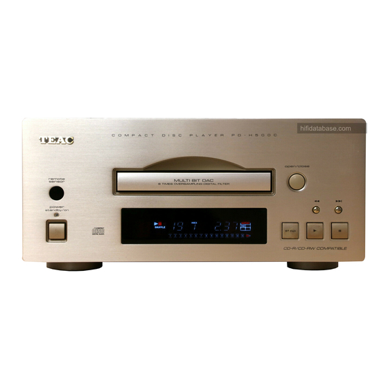
- Page 1 PD-H500C Compact Disc Player...
- Page 3 TC9432AF/ TC9462AF (Digital Signal Processor) PIN No. NAME FUNCTIONAL DESCRIPTION REMARKS Test mode terminal. Normally, keep at open. TEST0 With pull-up resistor. Playback speed mode flag output terminal. UHSO PLAYBACK SPEED Normal 2 times UHSO 4 times Subcode Q data emphasis flag output terminal. Emphasis ON at “H”...
- Page 5 PIN No. NAME FUNCTIONAL DESCRIPTION REMARKS This terminal controls IO0~IO3 terminal. At “L” level time, IO0, 1 out feed equalizer signal of DMOUT With pull-up resistor. 2-state PWM. IO2, 3 out disk equalizer signal of 2-state PWM. CKSE Normally, keep at open. With pull-up resistor.
- Page 6 TEST 0 XVDD UHSO Micom EMPH XVSS Interface LRCK 1bit Audio out circuit Correction circuit AOUT Clock TES IO1 DOUT generator MBOV TES I/N DACT CKSE SBOK DMOUT CLCK DATA SFSY SBSY SPCK FLGD SPDA FLGC COFS FLGB MONIT FLGA TESIO 0 A / D P2VREF...
-
Page 7: Function Description
TA2150FN PIN No. SYMBOL FUNCTION DESCRIPTION REMARKS Power supply input terminal. RF amplitude adjustment control signal input termi- 3 signals input. nal. RFGC (2VRO, VRo, GND) Controlled by 3-PWM signals. (PWM carrier = 88.2kHz) Open loop gain adjustment terminal for AGC amp. (Note 1) GMAD Connected to pin diode... - Page 8 TA2150FN PIN No. SYMBOL FUNCTION DESCRIPTION REMARKS Reference signal (VRO) output terminal. VRO = 2.1 V when Vcc = 5 V RFRP Track count signal output terminal. Time constant adjustment terminal for bottom Adjusted by capacitance. detection. RFCT RFRP signal center level output terminal. Time constant adjustment terminal for peak detec- Adjusted by capacitance.
- Page 9 SERVICE MANUAL...
- Page 11 SERVICE MANUAL...
- Page 13 EXPLODED VIEW LIST £ £ £ £ INCLUDED ACCESSORIES SERVICE MANUAL...
- Page 14 CD MAIN PCB ASSY CD MAIN PCB ASSY £ £ £ £ £ CD SUB PCB ASSY £ £ £ £ £ £ £ £ SERVICE MANUAL...
- Page 16 PD-H500C/PD-H300C SCHEMATIC DIAGRAM P P D D - - H H 5 5 0 0 0 0 C C / / P P D D - - H H 3 3 0 0 0 0 C C NOTES: INSTRUCTIONS FOR SERVICE PERSONNEL 1.
- Page 17 PD-H500C/PD-H300C SCHEMATIC DIAGRAM P P D D - - H H 5 5 0 0 0 0 C C / / P P D D - - H H 3 3 0 0 0 0 C C NOTES: INSTRUCTIONS FOR SERVICE PERSONNEL 1.
Need help?
Do you have a question about the PD-H500C and is the answer not in the manual?
Questions and answers