Table of Contents
Advertisement
Quick Links
This manual has been provided for the use of authorized YAMAHA Retailers and their service personnel.
It has been assumed that basic service procedures inherent to the industry, and more specifically YAMAHA Products, are already
known and understood by the users, and have therefore not been restated.
IMPORTANT:
The data provided is believed to be accurate and applicable to the unit(s) indicated on the cover. The research, engineering, and
service departments of YAMAHA are continually striving to improve YAMAHA products. Modifications are, therefore,
inevitable and specifications are subject to change without notice or obligation to retrofit. Should any discrepancy appear to exist,
please contact the distributor's Service Division.
WARNING:
IMPORTANT:
CONTENTS
To Service Personnel ........................................... 1
Front Panels ............................................................. 2
Rear Panels ......................................................... 3 – 4
Specifications ..................................................... 5 – 7
Internal View ............................................................ 8
Disassembly Procedures .................................... 8
Self Diagnosis Function ............................... 9 – 27
Amp Check ................................................................. 28
1 0 0 7 3 1
IMPORTANT NOTICE
Failure to follow appropriate service and safety procedures when servicing this product may result in personal
injury, destruction of expensive components, and failure of the product to perform as specified. For these
reasons, we advise all YAMAHA product owners that any service required should be performed by an
authorized YAMAHA Retailer or the appointed service representative.
The presentation or sale of this manual to any individual or firm does not constitute authorization, certification
or recognition of any applicable technical capabilities, or establish a principle-agent relationship of any
form.
Static discharges can destroy expensive components. Discharge any static electricity your body may have
accumulated by grounding yourself to the ground buss in the unit (heavy gauge black wires connect to this
buss).
Turn the unit OFF during disassembly and part replacement. Recheck all work before you apply power to the
unit.
Ic Data ................................................................ 29 – 42
Display Data .................................................... 43 – 44
Pin Connection DIAGRAM ..................................... 45
BLOCK DIAGRAM ................................................ 46 – 49
PRINTED CIRCUIT BOARD ................................. 50 – 73
SCHEMATIC DIAGRAM ....................................... 74 – 80
PARTS LIST ........................................................ 81 – 106
REMOTE CONTROL TRANSMITTER .............. 107 – 112
RX-V3000/RX-V3000RDS
AV RECEIVER
SERVICE MANUAL
Advertisement
Table of Contents

Related Manuals for Yamaha RX-V3000RDS


Summary of Contents for Yamaha RX-V3000RDS
-
Page 1: Service Manual
This manual has been provided for the use of authorized YAMAHA Retailers and their service personnel. It has been assumed that basic service procedures inherent to the industry, and more specifically YAMAHA Products, are already known and understood by the users, and have therefore not been restated. -
Page 2: To Service Personnel
RX-V3000/RX-V3000RDS TO SERVICE PERSONNEL 1. Critical Components Information Components having special characteristics are marked Z AC LEAKAGE EQUIPMENT and must be replaced with parts having specifications equal WALL TESTER OR OUTLET UNDER TEST EQUIVALENT to those originally installed. 2. Leakage Current Measurement (For 120V Models Only) -
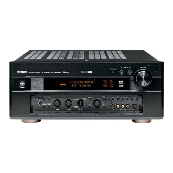
Page 3: Front Panels
RX-V3000/RX-V3000RDS FRONT PANELS RX-V3000 RX-V3000RDS... -
Page 4: Rear Panels
RX-V3000/RX-V3000RDS REAR PANELS RX-V3000 U model RX-V3000 C model RX-V3000 R, T models... - Page 5 RX-V3000/RX-V3000RDS RX-V3000 A model RX-V3000 L model RX-V3000RDS G model...
-
Page 6: Specifications
RX-V3000/RX-V3000RDS SPECIFICATIONS AUDIO SECTION Minimum RMS Output Power per Channel Residual Noise (IHF-A-Network) MAIN, 20Hz to 20kHz, 0.02% THD, 8Ω . . . 100W+100W MAIN L/R, SP OUT ......150µV Total Harmonic Distortion (20Hz to 20kHz) CENTER, 20Hz to 20kHz, 0.02% THD, 8Ω... - Page 7 RX-V3000/RX-V3000RDS FM SECTION U ..USA model C ..Canadian model Tuning Range U, C models ..... . . 87.5 to 107.9MHz A .
- Page 8 RX-V3000/RX-V3000RDS SET MENU TABLE SET MENU PRESET VALUE SETTING RANGES SPEAKER SET CENTER SPEAKER LARGE LARGE/SMALL/NONE MAIN SPEAKER LARGE LARGE/SMALL REAR L/R SPEAKER LARGE LARGE/SMALL/NONE REAR CT SPEAKER LARGE LARGE/SMALL/NONE LFE/BASS OUT BOTH SUBWOOFER/MAIN/BOTH FRONT EFFECT SPEAKER YES/NONE MAIN LEVEL NORMAL NORMAL/–10dB...
-
Page 9: Internal View
RX-V3000/RX-V3000RDS INTERNAL VIEW F AMP (2) P.C.B. MAIN (2) P.C.B. MAIN (4) P.C.B. F AMP (3) P.C.B. VIDEO (3) P.C.B. VIDEO (2) P.C.B. VIDEO (1) P.C.B. VIDEO (4) P.C.B. FUNCTION P.C.B. OPERATION (2) P.C.B. F AMP (1) P.C.B. MAIN (1) P.C.B. -
Page 10: Self Diagnosis Function
RX-V3000/RX-V3000RDS SELF DIAGNOSIS FUNCTION This product has a built-in self diagnosis function (DIAG) to facilitate inspection, measurement and determination of a faulty item, if any. There are 13 DIAG menu items each of which has sub-menu items. Listed in the table below are menu items and sub-menu items. - Page 11 RX-V3000/RX-V3000RDS DIAG menu Sub-menu Remote control code (key) IF STATUS 16. YSS2 --------- 17. YSS3 --------- DSP RAM CHECK DSP RAM check 7A---0A (CD SKIP +) SUM/VER/PORT 1. Version 7A---0D (CD REW) 2. Checksum (ALL/PROG) --------- 3. Checksum (232C/MAKER) --------- 4.
- Page 12 RX-V3000/RX-V3000RDS Display at the start of DIAG The diagnostic menu appears on the monitor screen. (It remains on display until it is canceled.) DIAGNOSTIC MENU 1.DSP THR 8.RS232C 2.HP ROUTE 9.PRESET 3.RAM THR 10.AD DATA 4.PRO LOGIC 11.STATUS 5.SP SET 12.DSP RAM...
- Page 13 RX-V3000/RX-V3000RDS In the case where the protection function works after DIAG has been started and the power is turned off ; When the protection function (*2) works, the history of the protection function appears on display and the power turns off. Repair the faulty parts according to the displayed history.
- Page 14 RX-V3000/RX-V3000RDS Operation procedure of DIAG menu and SUB-MENU There are No.1 to No.13 MENU items and some SUB-MENU items as well. DIAG menu selection Main unit: DSP PROGRAM selector (forward/reverse) Remote control unit: Cursor h(forward)/g(reverse) key SUB-MENU selection Main unit: EFFECT key (forward) Remote control unit: Cursor +(forward)/–(reverse) key...
- Page 15 RX-V3000/RX-V3000RDS Details of DIAG menu 1. DSP THROUGH There are 3 sub menu items (ANALOG BYPS, DSP 0dB, FULL BIT). ANALOG BYPS [Remote control code: 7A—90(PRG 9)] 1. DSP THROUGH • The input mode is fixed to use the analog (A/D) system.
- Page 16 RX-V3000/RX-V3000RDS DSP 0dB [Remote control code: 7A—91 (PRG 10)] 1. DSP THROUGH • The input signal is automatically identified and switched in the priority order of dts DOLBY DSP 0dB DIGITAL PCM AUDIO Analog (A/D) according to the signal detection.
- Page 17 RX-V3000/RX-V3000RDS FULL BIT [Remote control code: 7A—92 (PRG11)] 1. DSP THROUGH • The head margin is unused and the digital data is output in full bit. FULL BIT • The same applies as “DSP 0dB” except that the digital data is output in full bit at D/A but SWFR is not output in full bit.
- Page 18 RX-V3000/RX-V3000RDS (In the case of multi-ch source) • AC3D3 outputs signals using DOLBY DIGITAL/dts decode operation. AC3D3 YSS928 FILTER ANALOG CODEC DF1704 PCM1704 SDOA0 (A/D) MAIN AK4527 (Decoder) FILTER SUB DSP DF1704 PCM1704 DD/dts DECODER C/LFE SDOB0 FILTER DF1704 PCM1704...
- Page 19 RX-V3000/RX-V3000RDS 3. RAM THROUGH The input data is automatically identified and switched in the priority order of dts DOLBY DIGITAL PCM AUDIO Analog (A/D) according to the signal detection. The main L/R uses the analog through method when analog signals are input and the DSP through method when digital signals are input.
-
Page 20: Pro Logic
RX-V3000/RX-V3000RDS 4. PRO LOGIC The input signal is automatically identified and switched in the priority order of dts DOLBY DIGITAL PCM AUDIO Analog (A/D) according to the signal detection. The operation conforms to the ordinary DOLBY Normal sound field. YSS928 [Remote control code: 7A—0C (CD FF)]... - Page 21 RX-V3000/RX-V3000RDS 5. SPEAKERS SET The input signal is automatically identified and switched in the priority order of dts DOLBY DIGITAL PCM AUDIO Analog (A/D) according to the signal detection. There are seven sub-menu items. The signals output from the DSP are the same as 1. DSP THROUGH: DSP 0dB.
- Page 22 RX-V3000/RX-V3000RDS 6. DISPLAY CHK This program is used to check lighting of the FL display which changes as shown below according to operation of the sub-menu. The signals are processed using EFFECT OFF. (The L/R signals are output using ANALOG MAIN BYPASS set- ting.)
- Page 23 RX-V3000/RX-V3000RDS 7. MANUAL TEST The test noise is output by the noise generator with a built-in DSP from the channels specified by the sub-menu. There are ten sub-menu items. ALL [Remote control code: 7A—00 (TAPE PLAY)] 7. MANUAL TEST Noise is output from all channels.
- Page 24 RX-V3000/RX-V3000RDS 9. PRESET This menu reserves and inhibits initialization of the back-up RAM (parameter, set menu contents, etc. for the sound field program). The signals are processed using EFFECT OFF. (The L/R signals are output using ANALOG MAIN BYPASS set- ting.)
- Page 25 RX-V3000/RX-V3000RDS 10. FAN/AD The sub-menu of this menu displays the A/D conversion value of the CPU (function circuit board IC526) which detects the keys and protection functions of the main unit in %. (reference voltage 5V: 100%) It also displays the history of the fan being driven. When in KY0/KY1/RECOUT page, it is not possible to operate the keys of the main unit because the values of all keys are detected.
- Page 26 RX-V3000/RX-V3000RDS 11. IF STATUS (Input function status) Using this menu, the status data is displayed in the hexadecimal notation one after another. During signal processing, the status before execution of this menu is maintained. To convert the analog input to the digital input, use the following procedure.
- Page 27 RX-V3000/RX-V3000RDS 5th byte Indicate Indicates the information on the signal processing status. 0 0 0 0 0 0 0 0 bit7 MUTE requested 7 6 5 4 3 2 1 0 bit6 dts flashing (Red) bit5 EX sound field being processed...
- Page 28 RX-V3000/RX-V3000RDS 12. DSP RAM CHECK [Remote control code: 7A—0A (CD SKIP +)] This menu is used to self-diagnose whether or not YSS928 (IC501 of DSP circuit board) and external RAM (IC502 of DSP circuit board) are connected properly. During signal processing, the status before execution of this menu is maintained.
- Page 29 RX-V3000/RX-V3000RDS AMP CHECK Confirmation of Idling Current 1) No signal applied. 2) Non-loaded condition. 3) Aging is 10 minutes Test Point Item Rating (DC) Q58 Base – Emitter (MAIN [1] P.C.B.) MAIN L Q65 Base – Emitter (MAIN [1] P.C.B.) MAIN R Q72 Base –...
- Page 30 RX-V3000/RX-V3000RDS IC DATA IC526 : M30802SGP (FUNCTION P.C.B.) 16 bit µ-COM (CPU) P44/CS3/A20(MA12) P10/D8 P45/CS2/A21 P07/D7 P46/CS1/A22 P06/D6 P47/CS0/A23 P05/D5 P125 P04/D4 P126 P114 P127 P113 P50/WRL/WR/CASL P112 P51/WRH/BHE/CASH P111 P52/RD/DW P110 P53/BCLK/ALE/CLKOUT P03/D3 P130 P02/D2 P131 P01/D1 P00/D0 P132...
- Page 31 RX-V3000/RX-V3000RDS IC526 : M30802SGP (FUNCTION P.C.B.) 16 bit µ-COM (CPU) PORT Name Function Power On Power Off Backup TXD4 TXDR 232C Transmission Data 232C RTS out CTS4 232C CTS input Fan Control SDTN SDT for Non Audio RXRDS RDS Reception/Frequency Switch (Note 1)
- Page 32 RX-V3000/RX-V3000RDS IC526 : M30802SGP (FUNCTION P.C.B.) 16 bit µ-COM (CPU) PORT Name Function Power On Power Off Backup P133 /BEC Bass Extension Control Ground P132 /Z2MT ZONE2 Mute + 5V P131 /HPMT Head Phone Mute P130 /FMTF Full Mute (FL/FR)
- Page 33 RX-V3000/RX-V3000RDS IC526 : M30802SGP (FUNCTION P.C.B.) 16 bit µ-COM (CPU) PORT Name Function Power On Power Off Backup Data bus Data bus Data bus P114 /MLV Main Level Select (0/-10dB) P113 Power Relay P112 Speaker Relay Effect P111 Speaker Relay Main B...
- Page 34 RX-V3000/RX-V3000RDS IC501 : YSS928 (DSP P.C.B.) AC3D3 RAMA10 RAMD2 RAMA11 RAMD1 RAMD0 VDD2 VDD2 SELI8 SELI7 OPORT7 SELI6 OPORT6 SELI5 OPORT5 RAMA12 OPORT4 RAMA13 OPORT3 RAMA14 OPORT2 RAMA15 OPORT1 RAMA16 OPORT0 RAMA17 ZEROBF2L OVFB/END ZEROBF2R ZEROFLG ZEROBF3L ZEROBF3R NONPCM VDD1...
- Page 35 RX-V3000/RX-V3000RDS IC501 : YSS928 (DSP P.C.B.) AC3D3 Name Function Crystal oscillator connecting terminal Crystal oscillator connecting terminal (24.576MHz ) SELI1 Built-in selector input 1 (AXD) SELI0 Built-in selector input 0 (GND) SELOA Built-in selector output A (ISEL) SELOB Built-in selector output B...
- Page 36 RX-V3000/RX-V3000RDS IC501 : YSS928 (DSP P.C.B.) AC3D3 Name Function SDWCKI1 Word clock input terminal for SDIB, SDOB interface (Unconnected) SDBCKI1 Bit clock input terminal for SDIB, SDOB interface (Unconnected) Ground terminal SDOB3 PCM output terminal from Sub DSP SDOB2 PCM output terminal from Sub DSP...
- Page 37 RX-V3000/RX-V3000RDS IC501 : YSS928 (DSP P.C.B.) AC3D3 Name Function RAMA5 Sub DSP: External memory address terminal 5 RAMA2 Sub DSP: External memory address terminal 2 SELI13 Built-in selector input 13 (AC3RF) SELI12 Built-in selector input 12 (CXE) SELI11 Built-in selector input 11...
- Page 38 RX-V3000/RX-V3000RDS IC503 : PM4007A (DSP P.C.B.) AC-3 RF Demodulator AVDD CPIN CMIN AGND DOUT DOUTB WINGT SYST0 SYST1 ADST0 ADST1 BUNRI AGND AVDD Name Function Ground (0V) +5V power supply RESET System resetting terminal (reset at “L”) OSCON Oscillation control terminal. Oscillation ON at “H”, set to “H” normally and to “L” when in standby state...
- Page 39 RX-V3000/RX-V3000RDS IC503 : PM4007A (DSP P.C.B.) AC-3 RF Demodulator Name Function External RAM address output. Address 6 External RAM address output. Address 7 Ground terminal (0V) +5V power supply External RAM address output. Address 12 External RAM address output. Address 14 (MSB) External RAM write enable signal, active at “L”...
- Page 40 RX-V3000/RX-V3000RDS IC503 : PM4007A (DSP P.C.B.) AC-3 RF Demodulator Name Function AVDD +5V power supply for analog comparator CPIN Analog comparator input, positive side (Non-reverse side: QPSK input) CMIN Analog comparator input, negative side (reverse side) AGND Ground terminal for analog comparator (0V)
- Page 41 RX-V3000/RX-V3000RDS IC610 : LC74781-9798 (VIDEO P.C.B.) Superimpose VSS1 VDD1 XTAL IN XTAL OUT CTRL3 CTRL1 CTRL2 BLANK SEP IN OSC IN SEP OUT OSC OUT SEPC CHARA SYN IN VDD1 SCLK CV IN VDD2 CV OUT SERIAL 8 BIT LATCH...
- Page 42 RX-V3000/RX-V3000RDS IC610 : LC74781-9798 (VIDEO P.C.B.) Superimpose Pin No. Symbol Terminal name Function Ground terminal Connection to GND (Digital system ground terminal) VSS1 Crystal oscillation Terminal to connect the crystal of the crystal oscillator for internal synchronous XTAL IN terminal signal generation and a capacitor or to input an external clock.
- Page 43 RX-V3000/RX-V3000RDS Extension Port IC611 : BU2092 (VIDEO P.C.B.) 12-bit Serial In/Parallel Out Driver DATA CONTROL CLOCK CIRCUIT PORT Name Function Power On Power Off Backup Ground DATA DATA Serial Data Input CLOCK CLOCK Shift Clock of Data (Rise Edge Trigger)
-
Page 44: Display Data
RX-V3000/RX-V3000RDS DISPLAY DATA V901 : 32-BT-07G (V6291200) &0 PATTERN AREA PIN CONNECTION Note 1) F1, F2 ..Filament 3) P1A~P35A, P1B~P35B ..Datum Line 5) IC ....Internal connection 2) NP ....No Pin 4) 1GA~16GA, 1GB~16GB ....Grid 6) Fd terminals are to be supplied through 51kΩ from Ec. - Page 45 RX-V3000/RX-V3000RDS ANODE CONNECTION...
Need help?
Do you have a question about the RX-V3000RDS and is the answer not in the manual?
Questions and answers