Table of Contents
Advertisement
Quick Links
Advertisement
Table of Contents

Related Manuals for Supero X8SIE-F


Summary of Contents for Supero X8SIE-F
- Page 1 X8SIE X8SIE-F X8SI6-F X8SIE-LN4 X8SIE-LN4F USER’S MANUAL Revision 1.1...
- Page 2 This product, including software and docu- mentation, is the property of Supermicro and/or its licensors, and is supplied only under a license. Any use or reproduction of this product is not allowed, except as expressly permitted by the terms of said license.
-
Page 3: About This Motherboard
X8SIE/X8SIE-F/X8SI6-F/X8SIE-LN4/X8SIE-LN4F offers substantial enhancements in price/system performance ratio in a cost-effective, small form- factor package. Please refer to our web site (http://www.supermicro.com/products/) for updates on supported processors. This product is intended to be installed and serviced by professional technicians. -
Page 4: Contacting Supermicro
Super Micro Computer, Inc. 980 Rock Ave. San Jose, CA 95131 U.S.A. Tel: +1 (408) 503-8000 Fax: +1 (408) 503-8008 Email: marketing@supermicro.com (General Information) support@supermicro.com (Technical Support) Web Site: www.supermicro.com Europe Address: Super Micro Computer B.V. Het Sterrenbeeld 28, 5215 ML... -
Page 5: Table Of Contents
X8SIE/X8SIE-F/X8SI6-F/X8SIE-LN4/X8SIE-LN4F User’s Manual Table of Contents Preface About This Motherboard ....................3 Manual Organization ..................... 3 Conventions Used in the Manual: ................. 3 Contacting Supermicro ....................4 Chapter 1 Introduction Overview ......................1-1 Checklist ......................1-1 Motherboard Features ..................1-7 Chipset Overview ..................1-11... - Page 6 Table of Contents Memory Population Guidelines ..............2-11 Installing and Removing DIMMs ..............2-13 Tools Needed ....................2-15 Location of Mounting Holes ................2-15 Motherboard Installation ................2-15 Installation Instructions .................. 2-16 Connectors/IO Ports ..................2-17 Back Panel Connectors and IO Ports ............2-17 ATX PS/2 Keyboard and PS/2 Mouse Ports ..........
- Page 7 PCI Slot SMB Enable ................2-36 VGA Enable ....................2-37 SAS Enable/Disable (X8SI6-F Only) ............2-37 USB Wake-Up ..................2-38 BMC Enable (X8SIE-F/X8SI6- F/X8SIE-LN4F Only) ....... 2-38 Onboard Indicators ..................2-39 LAN LEDs ....................2-39 IPMI Dedicated LAN LEDs ..............2-39 Onboard Power LED ......................
- Page 8 Table of Contents Boot Settings ....................4-21 Exit Options ....................4-22 Appendix A POST Error Beep Codes Recoverable POST Error Beep Codes ..............A-1 Appendix B Software Installation Instructions Installing Drivers ....................B-1 Configuring Supero Doctor III .................B-2 Appendix C - BIOS Recovery C-1 Recovery Process from a USB Device/Drive (Recommended Method) .....C-1 C-2 Recovery Process from an IDE/SATA ATAPI Disc Drive ........C-2...
- Page 9 Quick-Start Guide Quick-Start Guide Install the Processor Install the Heatsink and Fan...
-
Page 10: Install The Memory Modules
Quick-Start Guide Install the Memory Modules Press Down Lock Lock Install the I/O Shield Note: Chassis and I/O plate images are for illustration purposes only. They may be different from what you have. - Page 11 Quick-Start Guide Install the Motherboard KB/MOUSE JPUSB1:B/P USB WAKE UP JPI2C:PWR I2C 1-2:ENABLE 2-3:DISABLE FLOPPY JPUSB1 JAR: PSU ALARM RST DDR3 1066/1333 UDIMM/RDIMM required FAN5 LAN1/LAN3 JPL1:LAN1 1-2:ENABLE 2-3:DISABLE JPL2:LAN2 1-2:ENABLE LAN2/LAN4 2-3:DISABLE JPL3:LAN3 1-2:ENABLE 2-3:DISABLE JPL4:LAN4 1-2:ENABLE 2-3:DISABLE JI2C1/JI2C2 ON:Enable OFF:Disable SLOT6 PCI-E 2.0 X16...
- Page 12 Quick-Start Guide Install Internal Peripherals IDE / Floppy Drives Add-on Cards SATA / SAS Drives Install External Peripherals Mouse LAN Ports VGA Port IPMI Port Serial Port (COM1) USB 0/1 Keyboard...
-
Page 13: Chapter 1 Introduction
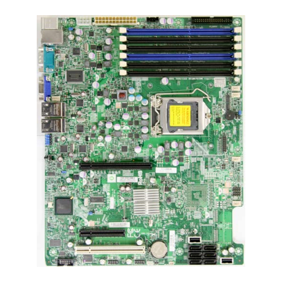
Checklist Congratulations on purchasing your computer motherboard from an acknowledged leader in the industry. Supermicro boards are designed with the utmost attention to detail to provide you with the highest standards in quality and performance. Please check that the following items have all been included with your motherboard. - Page 14 X8SIE/X8SIE-F/X8SI6-F/X8SIE-LN4/X8SIE-LN4F User’s Manual Motherboard (X8SIE-LN4F) Image Note: All graphics shown in this manual were based upon the latest PCB Revision available at the time of publishing of the manual. The motherboard you've received may or may not look exactly the same as the graphics...
- Page 15 Chapter 1: Introduction Motherboard Layout (X8SI6-F Shown) KB/MOUSE JPUSB1:B/P USB WAKE UP JPI2C:PWR I2C 1-2:ENABLE 2-3:DISABLE FLOPPY JPUSB1 JAR: PSU ALARM RST DDR3 1066/1333 UDIMM/RDIMM required FAN5 LAN1/LAN3 JPL1:LAN1 1-2:ENABLE 2-3:DISABLE JPL2:LAN2 1-2:ENABLE LAN2/LAN4 2-3:DISABLE JPL3:LAN3 1-2:ENABLE 2-3:DISABLE JPL4:LAN4 1-2:ENABLE 2-3:DISABLE JI2C1/JI2C2 ON:Enable...
- Page 16 X8SIE/X8SIE-F/X8SI6-F/X8SIE-LN4/X8SIE-LN4F User’s Manual KB/MOUSE JPUSB1:B/P USB WAKE UP JPI2C:PWR I2C 1-2:ENABLE 2-3:DISABLE FLOPPY JPUSB1 JAR: PSU ALARM RST DDR3 1066/1333 UDIMM/RDIMM required FAN5 LAN1/LAN3 JPL1:LAN1 1-2:ENABLE 2-3:DISABLE JPL2:LAN2 1-2:ENABLE LAN2/LAN4 2-3:DISABLE JPL3:LAN3 1-2:ENABLE 2-3:DISABLE JPL4:LAN4 1-2:ENABLE 2-3:DISABLE JI2C1/JI2C2 ON:Enable OFF:Disable SLOT6 PCI-E 2.0 X16...
- Page 17 LAN4 X8SIE-LN4F motherboards only) I-SATA 0~5 Serial ATA ports SAS 0~3, 4~7 Serial Attached SCSI (SAS) Ports (X8SI6-F Only) IPMI LAN IPMI LAN Port (X8SIE-F/X8SI6-F/X8SIE-LN4F Only) JPI2C PWR supply (I C) System Management Bus SPKR1 Internal speaker/buzzer JSPK Speaker header (Pins 3/4: Internal, 1~4:External)
- Page 18 X8SIE/X8SIE-F/X8SI6-F/X8SIE-LN4/X8SIE-LN4F User’s Manual Jumpers Jumper Description Default Number JPUSB1 USB0/1 Wake-up Pins 1-2 (Enabled) JBT1 CMOS Clear (See Chpt. 2) JPS1 SAS Enable Pins 1-2 (Enabled) C1/JI SMB to PCI Slots (See Chpt. 2) JPG1 Onboard VGA Enable Pins 1-2 (Enabled)
-
Page 19: Motherboard Features
512MB,1GB, 2GB, 4GB, and 8GB Chipset Intel® 3420 Chipset (Ibex Peak) Expansion Slots One (1) PCI-E 2.0 x16 slot (X8SIE/X8SIE-F/X8SIE-LN4/ X8SIE-LN4F) or one (1) PCI-E 2.0 x8 (x16 physical) (X8SI6-F) One (1) PCI-E 2.0 x4 (x8 physical) One (1) 32-bit PCI 33MHz slot. 5V for motherboard revi- sion 1.01 and below, 3.3V for motherboard revision 1.02... - Page 20 X8SIE/X8SIE-F/X8SI6-F/X8SIE-LN4/X8SIE-LN4F User’s Manual Floppy Disk Drive One (1) floppy drive interface (up to 1.44 MB) USB Devices Two (2) USB ports on the rear IO panel Four (4) USB devices via Two (2) USB header connectors for front access Two (2) Type A internal connectors...
- Page 21 Dimensions ATX form factor, 12" x 9.6" Note: For IPMI Configuration Instructions, please refer to the Embedded IPMI Configuration User's Guide available @ http://www.supermicro.com/ support/manuals/. *Supports RAID Key for RAID 5 which allows the RAID host adapter to in- terface with the LSI Mega-RAID firmware for enhanced RAID performance.
-
Page 22: Block Diagram
LPC I/O HEALTH INFO X8SIE-F/X8SI6-F/ X8SIE-LN4F Only X8SIE/X8SIE-F/X8SI6-F/X8SIE-LN4/X8SIE-LN4F System Block Diagram Note: This is a general block diagram and may not exactly represent the features on your motherboard. See the Motherboard Features pages for the actual specifications of each motherboard. 1-10... -
Page 23: Chipset Overview
The Intel 3420 chipset features a high-speed Direct Media Interface (DMI) for chip- to-chip true isochronous communication with the processor. This feature allows the X8SIE/X8SIE-F/X8SI6-F/X8SIE-LN4/X8SIE-LN4F to achieve up to 10 Gb/s of software-transparent data transfer in each direction, achieving better performance than comparable systems. -
Page 24: Pc Health Monitoring
X8SIE/X8SIE-F/X8SI6-F/X8SIE-LN4/X8SIE-LN4F User’s Manual PC Health Monitoring This section describes the PC health monitoring features of the X8SIE/X8SIE-F/ X8SI6-F/X8SIE-LN4/X8SIE-LN4F. These features are supported by an onboard System Hardware Monitor chip. Recovery from AC Power Loss BIOS provides a setting for you to determine how the system will respond when AC power is lost and then restored to the system. -
Page 25: Slow Blinking Led For Suspend-State Indicator
It is even more important for processors that have high CPU clock rates of 1 GHz and faster. X8SIE/X8SIE-F/X8SI6-F/X8SIE-LN4/X8SIE-LN4F accommodates ATX12V standard power supplies. Although most power supplies generally meet the specifications required by the CPU, some are inadequate. A 2-Amp of current supply on a 5V Standby rail is strongly recommended. -
Page 26: Super I/O
SMI or SCI function pin. It also features auto power management to reduce power consumption. iSCSI Support The X8SIE/X8SIE-F/X8SI6-F/X8SIE-LN4/X8SIE-LN4F motherboard supports the iSCSI Internet Protocol. iSCSI is an IP networking standard used to link and man- age data storage, and for data transfers across the internet/intranets through long distances. -
Page 27: 1-7 Overview Of The Winbond Wpcm450 Controller
X8SIE and the X8SIE-LN4 motherboards. Another version, the WPCM450-R also has all the features as described above plus IPMI 2.0 support. This particular chip is installed in the X8SIE-F, X8SI6-F and X8SIE-LN4F mother- board models. Note: For more information on IPMI configuration, please refer to the Embedded IPMI User's Guide posted on our website @ http://www.super-... -
Page 28: Chapter 2 Installation
Chapter 2: Installation Chapter 2 Installation Static-Sensitive Devices Electrostatic-Discharge (ESD) can damage electronic com ponents. To prevent dam- age to your system board, it is important to handle it very carefully. The following measures are generally sufficient to protect your equipment from ESD. Precautions •... -
Page 29: Processor And Heatsink Installation
CPU socket cap is in place and none of the socket pins are bent; otherwise, contact your retailer immediately. Refer to the Supermicro web site for updates on CPU support. Installing the LGA1156 Processor Press the load lever to release the load plate, which covers the CPU socket, from its locking position. - Page 30 Chapter 2: Installation Gently lift the load lever to open the load plate. Remove the plastic cap. Use your thumb and your index finger to hold the CPU at the top center edge and the bottom center edge of the CPU. Align the CPU key that is the semi-circle cutouts against the socket keys.
- Page 31 X8SIE/X8SIE-F/X8SI6-F/X8SIE-LN4/X8SIE-LN4F User's Manual Do not rub the CPU against the surface or against any pins of the socket to avoid damage to the CPU or the socket.) With the CPU inside the socket, inspect the four corners of the CPU to make sure that the CPU is properly installed.
-
Page 32: Installing A Passive Cpu Heatsink
Screw in two diagonal screws (i.e., the #1 and the #2 screws) until just snug (do not over-tighten the screws to avoid possible damage to the CPU.) Finish the installation by fully tightening all four screws. Recommended Supermicro heatsink: SNK-P0046P heatsink with BKT-0028L bottom bracket... -
Page 33: Removing The Heatsink
X8SIE/X8SIE-F/X8SI6-F/X8SIE-LN4/X8SIE-LN4F User's Manual Removing the Heatsink Warning: We do not recommend that the CPU or the heatsink be removed. However, if you do need to uninstall the heatsink, please follow the instruc- tions below to uninstall the heatsink to prevent damage done to the CPU or the CPU socket. -
Page 34: Installing An Active Fan Cpu Heatsink
If necessary, rearrange the wires to make sure that the wires are not pinched between the heatsink and the CPU. Also make sure to keep clearance between the fan wires and the fins of the heatsink. Recommended Supermicro heatsink: SNK-P0046A4 active heatsink... - Page 35 X8SIE/X8SIE-F/X8SI6-F/X8SIE-LN4/X8SIE-LN4F User's Manual Align the four heatsink fasteners with the mounting holes on the moth- erboard. Gently push the pairs of diagonal fasteners (#1 & #2, and #3 & #4) into the mounting holes until you hear a click. (Note: Make sure to orient each fastener so that the narrow end of the groove is pointing outward.)
- Page 36 Chapter 2: Installation Removing the Heatsink Warning: We do not recommend that the CPU or the heatsink be re- moved. However, if you do need to remove the heatsink, please follow the instructions below to uninstall the heatsink and prevent damage to the CPU or other components.
-
Page 37: System Memory
X8SIE/X8SIE-F/X8SI6-F/X8SIE-LN4/X8SIE-LN4F User's Manual System Memory Note: Check the Supermicro web site for recommended memory modules. CAUTION Exercise extreme care when installing or removing DIMM modules to prevent any possible damage. How to Install DIMMs Insert the desired number of DIMMs into the memory slots, starting with DIMM1A (DIMM A, Channel 1 - see Figure A on the following page). -
Page 38: Memory Population Guidelines
LAN1/LAN3 Memory Population Guidelines JPL1:LAN1 1-2:ENABLE 2-3:DISABLE JPL2:LAN2 1-2:ENABLE LAN2/LAN4 2-3:DISABLE JPL3:LAN3 1-2:ENABLE 2-3:DISABLE Please follow the tables below when populating the X8SIE/X8SIE-F/X8SI6-F/X8SIE- LN4/X8SIE-LN4F. JPL4:LAN4 1-2:ENABLE DDR3 ECC UDIMM Memory 2-3:DISABLE JI2C1/JI2C2 ON:Enable OFF:Disable DIMM Slots DIMMs DIMM Type POR Speeds Ranks per DIMM SLOT6 PCI-E 2.0 X16... - Page 39 X8SIE/X8SIE-F/X8SI6-F/X8SIE-LN4/X8SIE-LN4F User's Manual DDR3 ECC RDIMM Memory DIMM Slots DIMMs DIMM Type POR Speeds Ranks per DIMM per Channel Populated (any combination) per Channel Registered 1066, 1333 Single Rank, Dual DDR3 ECC Rank Registered 1066 Quad Rank DDR3 ECC Registered...
-
Page 40: Installing And Removing Dimms
Chapter 2: Installation Installing and Removing DIMMs Position the DIMM module's bottom key so it aligns with the receptive point on the slot. Notches Release Push the Lock/Release tabs to their Release po- sitions. Make sure that the DIMM module's side notches align with the slot's Lock/ Release Release tabs as it is pressed in. - Page 41 X8SIE/X8SIE-F/X8SI6-F/X8SIE-LN4/X8SIE-LN4F User's Manual Note: Due to memory allocation to system devices, the amount of memory that remains available for operational use will be reduced when 4 GB of RAM is used. The reduction in memory availability is disproportional. For Microsoft Windows users: Microsoft implemented a design change in Win- dows XP with Service Pack 2 (SP2) and Windows Vista.
-
Page 42: Tools Needed
Chapter 2: Installation Motherboard Installation All motherboards have standard mounting holes to fit different types of chassis. Make sure that the locations of all the mounting holes for both motherboard and chassis match. Although a chassis may have both plastic and metal mounting fas- teners, metal ones are highly recommended because they ground the motherboard to the chassis. -
Page 43: Installation Instructions
X8SIE/X8SIE-F/X8SI6-F/X8SIE-LN4/X8SIE-LN4F User's Manual Installation Instructions Install the I/O shield into the chassis. Note: Image is for illustration purposes only. Your particular chassis may be different. I/O Shield Locate the mounting holes on the motherboard. Refer to the layout on the previous page for mounting hole locations. -
Page 44: Connectors/Io Ports
I-SATA4 Back Panel Connectors 1. Keyboard (Purple) 7. VGA 2. PS/2 Mouse (Green) 8. LAN1 3. USB Port 0 9. LAN2 4. USB Port 1 10. LAN3 (X8SIE-LN4/X8SIE-LN4F) 5. IPMI LAN (X8SIE-F/X8SI6-F/ 11. LAN4 (X8SIE-LN4/X8SIE-LN4F) X8SIE-LN4F) 6. COM 1 2-17... -
Page 45: Atx Ps/2 Keyboard And Ps/2 Mouse Ports
X8SIE/X8SIE-F/X8SI6-F/X8SIE-LN4/X8SIE-LN4F User's Manual ATX PS/2 Keyboard and PS/2 PS/2 Keyboard/Mouse Pin Mouse Ports Definitions PS2 Keyboard PS2 Mouse The ATX PS/2 keyboard and PS/2 Pin# Definition Pin# Definition mouse are located next to the Back KB Data Mouse Data Panel USB Ports 0/1 on the mother-... -
Page 46: Universal Serial Bus (Usb)
Chapter 2: Installation Universal Serial Bus (USB) Back Panel USB 0/1 Pin Definitions Two Universal Serial Bus ports (USB Pin# Definition Pin# Definition 0/1) are located on the I/O back panel. Additional four USB header connec- USB_PN1 USB_PN0 tions, USB 2/3 and USB 10/11 are USB_PP1 USB_PP0 used to provide front chassis access. -
Page 47: Ethernet Ports
IPMI Dedicated LAN is also lo- (Yellow, +3V3SB) cated above the USB 0/1 ports on the TD1- Link 1000 LED X8SIE-F, X8SIE-LN4F and X8SI6-F to (Yellow, +3V3SB) provide a dedicated network connec- TD2+ Ground tion for IPMI 2.0 support. These ports... -
Page 48: Serial Ports
Chapter 2: Installation Serial Ports Serial Port Pin Definitions (COM1/COM2) A COM Port is located on the I/O Pin # Definition Pin # Definition back panel (COM 1) and a Serial port header (COM 2) is located next to Front Panel USB 10/11 header to provide front access. -
Page 49: Video Connector
X8SIE/X8SIE-F/X8SI6-F/X8SIE-LN4/X8SIE-LN4F User's Manual Video Connector A Video (VGA) connector is located next to the COM Port on the I/O backpanel. This connector is used to provide video and CRT display. Refer to the board layout below for the location. 1. VGA... -
Page 50: Front Control Panel
These connectors are designed specifically for use with Supermicro server chassis. See the figure below for the descriptions of the various control panel buttons and LED indicators. Refer to the following section for descriptions and pin definitions. -
Page 51: Front Control Panel Pin Definitions
X8SIE/X8SIE-F/X8SI6-F/X8SIE-LN4/X8SIE-LN4F User's Manual Front Control Panel Pin Definitions Power LED Power LED Pin Definitions (JF1) The Power LED connection is located Pin# Definition on pins 15 and 16 of JF1. Refer to the table on the right for pin definitions. Ground HDD LED The HDD LED onnections are located... -
Page 52: Nic1/Nic2 (Lan1/Lan2)
Chapter 2: Installation NIC1/NIC2 (LAN1/LAN2) LAN1/LAN2 LED Pin Definitions (JF1) The NIC (Network Interface Control- Pin# Definition ler) LED connection for LAN port 1 is 9/11 located on pins 11 and 12 of JF1, and 10/12 Ground the LED connection for LAN Port 2 is on Pins 9 and 10. -
Page 53: Power Fail Led
X8SIE/X8SIE-F/X8SI6-F/X8SIE-LN4/X8SIE-LN4F User's Manual Power Fail LED PWR Fail LED Pin Definitions (JF1) The Power Fail LED connection is Pin# Definition located on pins 5 and 6 of JF1. Refer to the table on the right for pin defini- Ground tions. Reset Button... -
Page 54: Connecting Cables
Chapter 2: Installation Connecting Cables This section provides brief descriptions and pin-out definitions for onboard headers and connectors. Be sure to use the correct cable for each header or connector. • For information on Backpanel USB and Front Panel USB ports, refer to Page 2-19. -
Page 55: Fan Headers
X8SIE/X8SIE-F/X8SI6-F/X8SIE-LN4/X8SIE-LN4F User's Manual Fan Headers The X8SIE/X8SIE-F/X8SI6-F/X8SIE-LN4/ Fan Header X8SIE-LN4F has five fan headers (Fan1 ~ Pin Definitions Fan5). These fans are 4-pin fan headers. Pin# Definition However, Pins 1-3 of the fan headers are Ground (Black) backward compatible with the traditional 3-pin 2.5A/+16V... -
Page 56: Internal Buzzer
Chapter 2: Installation Internal Buzzer Internal Buzzer Pin Definition The Internal Buzzer (SPKR1) can be Pin# Definitions used to provide audible indications for Pin 1 Pos. (+) Beep In various beep codes. See the table on Pin 2 Neg. (-) Alarm the right for pin definitions. -
Page 57: Onboard Power Led
X8SIE/X8SIE-F/X8SI6-F/X8SIE-LN4/X8SIE-LN4F User's Manual Onboard Power LED Onboard PWR LED Pin Definitions An onboard Power LED header is Pin# Definition located at JLED. This Power LED header is connected to Front Control No Connection Panel located at JF1 to indicate the Connection to PWR status of system power. -
Page 58: T-Sgpio 0/1 Headers
Chapter 2: Installation T-SGPIO 0/1 Headers Serial_Link-SGPIO Two T-SGPIO (Serial-Link General Pur- Pin Definitions pose Input/Output) headers are located Pin# Definition Definition near the SAS connectors on the mother- board. These headers are used to com- Ground DATA Out municate with the enclosure management Load Ground chip in the system. -
Page 59: Wake-On-Lan
X8SIE/X8SIE-F/X8SI6-F/X8SIE-LN4/X8SIE-LN4F User's Manual Wake-On-LAN Wake-On-LAN Pin Definitions The Wake-On-LAN header is located at (JWOL) JWOL on the motherboard. See the table on Pin# Definition the right for pin definitions. (You must also +5V Standby have a LAN card with a Wake-On-LAN con- Ground nector and cable to use this feature.) -
Page 60: Unit Id Switch
Chapter 2: Installation Unit ID Switch UID Switch There are three Unit Identification (UID) Pin# Definition devices on the motherboard. A rear UID Ground switch and a rear UID LED indicator. The Ground Front Panel UID LED is connected to a Button In pin in the Front Control Panel (Pin 7 of Ground... -
Page 61: I-Button Raidkey Header
X8SIE/X8SIE-F/X8SI6-F/X8SIE-LN4/X8SIE-LN4F User's Manual I-Button RAIDKey Header I-Button for RAIDKey (JIBTN) An I-Button header (JIBTN), located near Pin Definition USB4, provides support for R AIDKey Pin# Definition which will allow the HostRAID to interface RAIDKey with the LSI Mega-RAID firmware for Ground RAID performance enhancement. -
Page 62: Jumper Settings
Chapter 2: Installation Jumper Settings Explanation of Jumpers To modify the operation of the motherboard, jumpers can be used to choose between optional settings. Jumpers create shorts be- tween two pins to change the function of the connector. Pin 1 is identified with a square solder pad on the printed circuit board. -
Page 63: Cmos Clear
X8SIE/X8SIE-F/X8SI6-F/X8SIE-LN4/X8SIE-LN4F User's Manual CMOS Clear JBT1 is used to clear CMOS. Instead of pins, this "jumper" consists of contact pads to prevent accidental clearing of CMOS. To clear CMOS, use a metal object such as a small screwdriver to touch both pads at the same time to short the connection. -
Page 64: Vga Enable
Chapter 2: Installation VGA Enable VGA Enable/Disable Jumper Settings (JPG1) JPG1 allows you to enable or disable Both Jumpers Definition the onboard VGA connector. The default Pins 1-2 Enabled position is on pins 1 and 2 to enable Pins 2-3 Disabled VGA. -
Page 65: Usb Wake-Up
Disabled, remove the USB devices from the USB ports whose USB jumper is Disabled before the sys- tem goes into the standby mode. BMC Enable (X8SIE-F/X8SI6- F/X8SIE- BMC IPMI Enable/Disable Jumper LN4F Only) Settings JPB is used to enable or disable the BMC... -
Page 66: Onboard Indicators
IPMI LAN Link LED (Left) & Activity LED (Right) In addition to LAN ports, an IPMI Dedi- Color Status Definition cated LAN is also located on the X8SIE-F/ Link (Left) Green: Solid 100 Mbps X8SI6-F./X8SIE-LN4F The yellow LED on Activity... -
Page 67: Onboard Power Led
System off and PWR Cable Connected or installing any component. See the layout below for the LED location. IPMI Heartbeat LED (X8SIE-F/X8SI6-F/ X8SIE-LN4F only) IPMI Heartbeat LED Indicator (LE7) LED Settings An IPMI Heartbeat LED is located at... -
Page 68: Sas Heartbeat Led & Sas Error Led (X8Si6-F Only)
Chapter 2: Installation SAS Heartbeat LED & SAS Error LED SAS Heartbeat LED (X8SI6-F only) Color Status Definition An Onboard SAS Heartbeat LED is located Green Blinking Normal at LE6 on the motherboard. When LE6 is blinking, SAS is functioning normally. When SAS Error LED the SAS Error LED (LE8) is on, a SAS error has occurred. -
Page 69: Sata, Sas And Floppy Drive Connections
X8SIE/X8SIE-F/X8SI6-F/X8SIE-LN4/X8SIE-LN4F User's Manual SATA, SAS and Floppy Drive Connections SATA Connectors SATA Connections Pin Definitions Six Serial ATA (SATA) connectors (I-SATA Pin# Signal 0~5) are located on the motherboard. These Ground Serial Link connections provide faster data SATA_TXP transmission than legacy Parallel ATA. See SATA_TXN the table on the right for pin definitions. -
Page 70: Floppy Connector
Chapter 2: Installation Floppy Connector Floppy Drive Connector Pin Definitions The floppy connector is located next Pin# Definition Pin # Definition to the DIMM memory banks on the Ground FDHDIN motherboard. See the table on the Ground Reserved right for pin definitions. FDEDIN Note the following when con- Ground... -
Page 71: Chapter 3 Troubleshooting
Chapter 3: Troubleshooting Chapter 3 Troubleshooting Troubleshooting Procedures Use the following procedures to troubleshoot your system. If you have followed all of the procedures below and still need assistance, refer to the ‘Technical Support Procedures’ and/or ‘Returning Merchandise for Service’ section(s) in this chapter. Always disconnect the AC power cord before adding, changing or installing any hardware components. -
Page 72: Memory Errors
Before contacting Technical Support, please make sure that you have followed all the steps listed below. Also, Note that as a motherboard manufacturer, Supermicro does not sell directly to end users, so it is best to first check with your distributor or reseller for troubleshooting services. -
Page 73: Frequently Asked Questions
3. If you've followed the instructions above to troubleshoot your system, and still cannot resolve the problem, then contact Supermicro's technical support and provide them with the following information: • Motherboard model and PCB revision number •... - Page 74 X8SIE/X8SIE-F/X8SI6-F/X8SIE-LN4/X8SIE-LN4F User's Manual BIOS warning message and the information on how to update your BIOS on our web site. Select your motherboard model and download the BIOS (.rom) file to your computer. Also, check the current BIOS revision and make sure that it is newer than your BIOS before downloading.
- Page 75 USB floppy drive instead of the onboard floppy drive. For the IPMI jumper location, please check Chapter 1. Question: Why can't I format a floppy disk in Windows or why does it take too long to format a floppy disk on the X8SIL-F or X8SIE-F/X8SI6-F moth- erboard? Answer: This is maybe because C State Technology is enabled in the BIOS.
-
Page 76: Battery Removal And Installation
X8SIE/X8SIE-F/X8SI6-F/X8SIE-LN4/X8SIE-LN4F User's Manual Battery Removal and Installation Battery Removal To remove the onboard battery, follow the steps below: Battery Lock Power off your system and unplug Battery your power cable. Locate the onboard battery as shown Battery Holder on the right. -
Page 77: Returning Merchandise For Service
You can obtain service by calling your vendor for a Returned Merchandise Authorization (RMA) number. (For faster service, you may also obtain RMA authorizations online (http://www.supermicro. com/support/rma/). When returning to the manufacturer, the RMA number should be prominently displayed on the outside of the shipping carton, and mailed prepaid or hand-carried. - Page 78 X8SIE/X8SIE-F/X8SI6-F/X8SIE-LN4/X8SIE-LN4F User's Manual Notes...
-
Page 79: Chapter 4 Bios
When an option is selected in the left frame, it is highlighted in white. Often a text message will accompany it. (Note: the AMI BIOS has default text messages built in. Supermicro retains the option to include, omit, or change any of these text messages.) The AMI BIOS Setup Utility uses a key-based navigation system called "hot keys". -
Page 80: How To Start The Setup Utility
Warning! Do not upgrade the BIOS unless your system has a BIOS-related issue. Flashing the wrong BIOS can cause irreparable damage to the system. In no event shall Supermicro be liable for direct, indirect, special, incidental, or consequential damages arising from a BIOS update. If you have to update the BIOS, do not shut down or reset the system while the BIOS is updating. - Page 81 <Tab> key or the arrow keys to move between fields. The date must be entered in Day MM/DD/YY format. The time is entered in HH:MM:SS format. (Note: The time is in the 24-hour format. For example, 5:30 P.M. appears as 17:30:00.) Supermicro X8SIE/X8SIE-F/X8SI6-F/X8SIE-LN4/X8SIE-LN4F Version Build Date...
-
Page 82: 4-3 Advanced Setup Configurations
X8SIE/X8SIE-F/X8SI6-F/X8SIE-LN4/X8SIE-LN4F 4-3 Advanced Setup Configurations Use the arrow keys to select Boot Setup and hit <Enter> to access the submenu items: BOOT Feature Quick Boot If Enabled, this option will skip certain tests during POST to reduce the time needed for system boot. The options are Enabled and Disabled. - Page 83 Chapter 4: AMI BIOS Wait For 'F1' If Error This forces the system to wait until the 'F1' key is pressed if an error occurs. The options are Disabled and Enabled. Hit 'Del' Message Display This feature displays "Press DEL to run Setup" during POST. The options are Enabled and Disabled.
- Page 84 X8SIE/X8SIE-F/X8SI6-F/X8SIE-LN4/X8SIE-LN4F ting. Select Auto for the BIOS to automatically select the CPU multiplier setting for your system. The options are Default and Manual. Clock Spread Spectrum Select Enable to use the feature of Clock Spectrum, which will allow the BIOS to monitor and attempt to reduce the level of Electromagnetic Interference caused by the components whenever needed.
- Page 85 Chapter 4: AMI BIOS Simultaneous Multi-Threading (Available when supported by the CPU) Set to Enabled to use the Hyper-Threading Technology, which will result in increased CPU performance. The options are Disabled and Enabled. Active Processor Cores Set to Enabled to use a processor's Second Core and beyond. (Please refer to Intel's web site for more information.) The options are All, 1, 2, 3 and 4.
-
Page 86: Advanced Chipset Control
X8SIE/X8SIE-F/X8SI6-F/X8SIE-LN4/X8SIE-LN4F Advanced Chipset Control The items included in the Advanced Settings submenu are listed below. Memory Remap Feature This feature when enabled, allows the remapping of everlapped PCI memory above the total physical memory. The settings are Enabled and Disabled. - Page 87 Chapter 4: AMI BIOS SATA#1 Configuration If Compatible is selected, it sets SATA#1 to legacy compatibility mode, while se- lecting Enhanced sets SATA#1 to native SATA mode. The options are Disabled, Compatible, Enhanced. Configure SATA as This feature allows the user to select the drive type for SATA#1. The options are IDE, RAID and AHCI.
- Page 88 X8SIE/X8SIE-F/X8SI6-F/X8SIE-LN4/X8SIE-LN4F Block (Multi-Sector Transfer) Block Mode boosts the IDE drive performance by increasing the amount of data transferred. Only 512 bytes of data can be transferred per interrupt if Block Mode is not used. Block Mode allows transfers of up to 64 KB per interrupt. Select Disabled to allow data to be transferred from and to the device one sector at a time.
- Page 89 Chapter 4: AMI BIOS Select MWDMA2 to allow the BIOS to use Multi-Word DMA mode 2. It has a data transfer rate of 16.6 MBs. Select UDMA0 to allow the BIOS to use Ultra DMA mode 0. It has a data transfer rate of 16.6 MBs.
- Page 90 X8SIE/X8SIE-F/X8SI6-F/X8SIE-LN4/X8SIE-LN4F PCI Latency Timer This feature sets the latency Timer of each PCI device installed on a PCI bus. Select 64 to set the PCI latency to 64 PCI clock cycles. The options are 32, 64, 96, 128, 160, 192, 224 and 248.
- Page 91 This feature allows the user decide which serial port to be used for Console Redirection. The options are COM 1, COM 2 and COM 3. Note: Serial Over LAN (SOL) is enabled on COM 3 on the X8SIE-F and X8SI6-F.
-
Page 92: Hardware Health Configuration
X8SIE/X8SIE-F/X8SI6-F/X8SIE-LN4/X8SIE-LN4F VT-UTF8 Combo Key Support A terminal keyboard definition that provides a way to send commands from a remote console. Available options are Enabled and Disabled. Sredir Memory Display Delay This feature defines the length of time in seconds to display memory information. - Page 93 Chapter 4: AMI BIOS Low – This level is considered as the ‘normal’ operating state. The CPU temperature is well below the CPU ‘Temperature Tolerance’. The motherboard fans and CPU will run normally as configured in the BIOS (Fan Speed Control). User intervention: No action required.
- Page 94 X8SIE/X8SIE-F/X8SI6-F/X8SIE-LN4/X8SIE-LN4F Supermicro has leveraged this feature by assigning a temperature status to certain thermal conditions in the processor (Low, Medium and High). This makes it easier for the user to understand the CPU’s temperature status, rather than by just simply seeing a temperature reading (i.e., 25 The information provided above is for your reference only.
- Page 95 The options are ACPI v1.0, ACPI v2.0 and ACPI v3.0. Please refer to ACPI's website for further explanation: http://www.acpi.info/ IPMI Configuration (X8SIE-F/X8SI6-F Only) Intelligent Platform Management Interface (IPMI) is a set of common interfaces that IT administrators can use to monitor system health and to manage the system as a whole.
- Page 96 X8SIE/X8SIE-F/X8SI6-F/X8SIE-LN4/X8SIE-LN4F IPMI Firmware Revision This item displays the current IPMI firmware revision. Status of BMC Baseboard Management Controller (BMC) manages the interface between system management software and platform hardware. This is an informational feature which returns the status code of the BMC micro controller.
- Page 97 Chapter 4: AMI BIOS Gateway Address - Enter the Gateway address this machine will use (i.e., 192.168.10.1). MAC Address - The BIOS will automatically enter the MAC address (also known as Hardware Address) of this machine, however it may be over-ridden. MAC addresses are 6 two-digit hexadecimal numbers (Base 16, 0 ~ 9, A, B, C, D, E, F) separated by dots.
-
Page 98: Security Settings
X8SIE/X8SIE-F/X8SI6-F/X8SIE-LN4/X8SIE-LN4F Security Settings The AMI BIOS provides a Supervisor and a User password. If you use both pass- words, the Supervisor password must be set first. Supervisor Password This item indicates if a supervisor password has been entered for the system. Clear means such a password has not been used and Set means a supervisor password has been entered for the system. -
Page 99: Boot Settings
Chapter 4: AMI BIOS Clear User Password (Available only if User Password has been set) Password Check Available options are Setup and Always. Boot Sector Virus Protection When Enabled, the AMI BOIS displays a warning when any program (or virus) is- sues a Disk Format command or attempts to write to the boot sector of the hard disk drive. -
Page 100: Exit Options
X8SIE/X8SIE-F/X8SI6-F/X8SIE-LN4/X8SIE-LN4F Hard Disk Drives This feature allows the user to specify the sequence of priority from the available Hard Drives. • 1st Drive [SATA: XXXXXXXXXX] • 2nd Drive [SATA: XXXXXXXXXX] Removable Drives This feature allows the user to specify the boot sequence from available Removable Drives. - Page 101 Chapter 4: AMI BIOS Save Changes and Exit When you have completed the system configuration changes, select this option to leave the BIOS Setup Utility and reboot the computer, so the new system con- figuration parameters can take effect. Select Save Changes and Exit from the Exit menu and press <Enter>.
- Page 102 X8SIE/X8SIE-F/X8SI6-F/X8SIE-LN4/X8SIE-LN4F Notes 4-24...
-
Page 103: Appendix A Post Error Beep Codes
Appendix A: POST Error Beep Codes Appendix A POST Error Beep Codes This section lists POST (Power On Self Test) error beep codes for the AMI BIOS. POST error beep codes are divided into two categories: recoverable and terminal. This section lists Beep Codes for recoverable POST errors. Recoverable POST Error Beep Codes When a recoverable type of error occurs during POST, BIOS will display a POST code that describes the problem. - Page 104 X8SIE/X8SIE-F/X8SI6-F/X8SIE-LN4/X8SIE-LN4F User's Manual Notes...
-
Page 105: Appendix B Software Installation Instructions
To install these software programs and drivers, click the icons to the right of these items. (Note: To install the Windows Operating System, please refer to the instructions posted on our website at http://www.supermicro.com/ support/manuals/.) Driver/Tool Installation Display Screen Note: Click the icons showing a hand writing on the paper to view the readme files for each item. -
Page 106: Configuring Supero Doctor Iii
X8SIE/X8SIE-F/X8SI6-F/X8SIE-LN4/X8SIE-LN4F User's Manual B-2 Configuring Supero Doctor III The Supero Doctor III program is a Web-base management tool that supports remote management capability. It includes Remote and Local Management tools. The local management is called the SD III Client. The Supero Doctor III program included on the CDROM that came with your motherboard allows you to monitor the environment and operations of your system. - Page 107 Supero Doctor III Interface Display Screen-II (Remote Control) Note: SD III Software Revision 1.0 can be downloaded from our Web site at: ftp://ftp.supermicro.com/utility/Supero_Doctor_III/. You can also download SDIII User's Guide at: http://www.supermicro.com/PRODUCT/ Manuals/SDIII/UserGuide.pdf. For Linux, we will still recommend that you...
- Page 108 X8SIE/X8SIE-F/X8SI6-F/X8SIE-LN4/X8SIE-LN4F User's Manual Notes...
-
Page 109: Appendix C - Bios Recovery
The recovery procedure described in this section is to be used only when advised by your Supermicro Technical Support representative, or in cases of emergencies where the system no longer can boot due to a corrupted BIOS. DO NOT re-program (re-flash) the BIOS if your system is running properly. -
Page 110: Recovery Process From An Ide/Sata Atapi Disc Drive
X8SIE/X8SIE-F/X8SI6-F/X8SIE-LN4/X8SIE-LN4F User’s Manual When the Boot Sector Recovery Process is complete, the system will reboot automatically and you will see a checksum error on your screen. Part 2: BIOS Reprogramming (Re-Flashing) After completing the Boot Sector Recovery Process, you will need to reprogram (“re-flash”) the proper BIOS binary file again into the BIOS ROM in order to have... - Page 111 (Disclaimer Continued) The products sold by Supermicro are not intended for and will not be used in life support systems, medical equipment, nuclear facilities or systems, aircraft, aircraft devices, aircraft/emergency communication devices or other critical systems whose failure to perform be reasonably expected to result in significant injury or loss of life or catastrophic property damage.
Need help?
Do you have a question about the X8SIE-F and is the answer not in the manual?
Questions and answers