Sony UP-895 Service Manual
Video graphic printer
Hide thumbs
Also See for UP-895:
- Instructions for use manual (108 pages) ,
- Specfications (2 pages) ,
- Catalog (46 pages)
Table of Contents
Advertisement
Advertisement
Table of Contents

Related Manuals for Sony UP-895


Summary of Contents for Sony UP-895
- Page 1 VIDEO GRAPHIC PRINTER UP-895 UP-895CE UP-895MD SERVICE MANUAL 1st Edition...
- Page 2 Ce manual est destiné uniquement aux personnes compétentes en charge de l’entretien. Afin de réduire les risques de décharge électrique, d’incendie ou de blessure n’effectuer que les réparations indiquées dans le mode d’emploi à moins d’être qualifié pour en effectuer d’autres. Pour toute réparation faire appel à une personne compétente uniquement. UP-895/(E)
-
Page 3: Table Of Contents
Memory and Head Control Circuit ............. 4-4 4-3-1. Reading the Serial Data from System Control ......4-5 4-3-2. Writing in Frame Memory ............4-5 4-3-3. Transfer from Frame Memory to Line Memory ......4-5 4-3-4. Thermal Head Control and One-Line Memory ......4-5 UP-895/(E) - Page 4 Door (Opening and Closing) is Out of Order ..........5-6 6. Service Mode (Self-diagnostic Function) Printing the Test Pattern ................6-1 6-2. Up/Down Operation of Head ..............6-2 6-3. Feed Operation .................... 6-2 6-4. Display and Clearing of Print Sheet History ..........6-3 7. Semiconductor Pin Assignments UP-895/(E)
- Page 5 Exploded Views ..................8-2 8-3. Electrical Parts List ..................8-7 9. Block Diagram Overall ........................9-1 10. Schematic Diagrams and Board Layouts FRAME ........................ 10-2 KY-454 ......................... 10-2 SE-531 ........................10-2 SE-532 ........................10-2 SU-52 ........................10-2 MA-99 ........................10-4 UP-895/(E)
- Page 7 3-868-286-01 (1) Video Graphic Printer Instructions for Use Page 20 For UP-895MD/895CE) UP-895 UP-895MD UP-895CE © 1999 Sony Corporation...
- Page 8 Table of Contents Overview WARNING For UP-895MD/895CE The UP-895/895MD/895CE is a black and white video Introduction Important safeguards/notices for use in the To prevent fire or shock hazard, do not expose the unit to graphics printer that can be used to print images rain or moisture.
-
Page 9: Setting Up The Printer
Connection/Setting Up the Printer Setting Up the Printer B GAMMA switch Setting the DIP Switches on the Connection Setting Up the Printer Sets the tone of printouts (density gradation). Rear Panel I: Soft gradation II: Standard You can set the printer to the desired specifications using To change the DIP switch settings Notes III: Hard gradation... - Page 10 Use only UPP-110S/110HD/110HG paper as FRAME (SW-DOWN): Normally keep this switch set chloride to touch printouts. Alcohol, plastic tape or specified for the UP-895/895MD/895CE. If another to this position. film will cause the printout to fade. type of paper is used, the quality of the printout FIELD (SW-UP): When printing fast-moving images •...
-
Page 11: Loading Paper
Loading Paper Printing To stop printing and print another image Loading Paper Printing displayed on the video monitor To do this, DIP Switch 1 (INTERRUPT) must be set to ON (SW-DOWN). (See page 24.) Before making printouts Notes Press the PRINT button while printing or copying. The •... - Page 12 Printing Printing Selecting the Printing Direction/ Making copies of the last printout Variations of printouts Image size Printing direction selector position Image Size selector Press the COPY button. The printer makes a copy of the Printouts obtained by the combination of the position SIDE last printout.
- Page 13 Precautions/Maintenance Printing Adjusting the Contrast and To adjust the brightness Precautions Maintenance You can adjust the brightness of printouts using the Brightness BRIGHT control. To make the image brighter, turn the BRIGHT control You can adjust the contrast and brightness of the clockwise.
-
Page 14: Specifications
Maintenance/Specifications Specifications Close the door by pushing it. REMOTE (stereo minijack) Specifications Press the FEED button and keep it pressed. When the buzzer sounds and the printer start ejecting Power requirements and consumption the cleaning sheet, release the FEED button. 100 to 120 V AC, 50/60 Hz, 1.5 A 1 GND 220 to 240 V AC, 50/60 Hz, 0.8 A... - Page 15 Is DIP Switch qa (INPUT) set to B & letters on the screen W when the input signal is a black printer and contact your Sony dealer or local authorized are not printed and white signal? (page 25) 3 STD (standard)/SIDE selector (28, 29) Sony service facility.
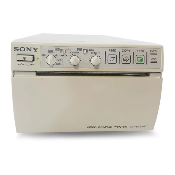
- Page 16 Location and Function of Parts qa OPEN button (26, 31) Back Opens or closes the door. Also, interrupts printing midway. Equipotential terminal (only for UP-895MD/ When the door is open, you can see the slide 895CE) switches in the paper tray. Used to connect to the equipotential plug to bring the various parts of a system to the same potential.
-
Page 17: Service Information
MA-99 board Remove the top cover in the order shown in the figure during removal. SE-532 board Removal of Top Cover 2 Top cover 1 M3 case fixing screw SU-52 board SE-531 board KY-454 board 1 M3 case fixing screw UP-895/(E) -
Page 18: Removal Of Major Parts
1 CN14 6 Power switch rod 1 CN1 Be careful not to slacken the harness when installing the mechanical block. 2 Screws (BVTT 3x6) 2 Screw (BVTT 3x6) 3 Claws 3 Claws 4 Front panel 2 Screws (BVTT 3x6) UP-895/(E) -
Page 19: Removal Of Ma-99 Board
5 Tapping screws (M3) 6 Switching 4 CN14 4 CN1 regulator 4 CN2 4 CN12 5 Tapping 4 CN8 screws (M3) 4 CN13 4 Screws 4 CN9 (PS 3x6) 4 CN3 4 Screws (PS 3x6) 4 CN7 6 MA-99 board UP-895/(E) -
Page 20: Removal Of Thermal Head
1 Screw (BVTT 3x6) 2 Top chassis 3 Heat sink 1 Screw (BVTT 3x6) 1 Flat type wire (26 core) Printing side 4 CN13 Spring compression 4 CN9 Contact 5 Head assembly 1 Flat type wire (30 core) 4 Thermal head UP-895/(E) -
Page 21: Tightening The Screws
Confirm that no clearance exists between the mechanical 1. Be careful not to hold the gear bracket by hand when installing screws 1 and 2. chassis and top chassis. 2. Confirm that the belt tension is not loosened after screw installation. UP-895/(E) -
Page 22: Installation Of Fan Motor
2-5. Installation of Fan Motor Install the fan motor while paying the attention to the direction of the harness with the surface, to which the fan motor sticker is attached, down. Screws (PTT 3x10) Fan motor MA-99 board Top chassis UP-895/(E) -
Page 23: Electrical Alignment
!= on the rear panel to ON, if 1RV4/MA-99 (C-2) connected, set to OFF. . Adjust RV4 (AGC OFF CONT) using 10 MA-99 steps signal input. 1.0 V 1RV4 Adjust so that video signal level is 1.0 V. UP-895/(E) -
Page 24: Brightness And Contrast Adjustment
MA-99 1RV5 1RV6 AD IN (TP6) (TP8) Adjust RV6 so that mid voltage between 0 and 1 is equaled to the VRB voltage. Adjust RV5 so that mid voltage between 9 and 10 is equaled to the VRT voltage. UP-895/(E) -
Page 25: Head Voltage Adjustment
. Set the POWER switch to ON while Release the buttons when the buzzer sounds Nothing pressing the PRINT, COPY, and FEED three times. The initialization of print count buttons. history is then completed (becomes zero in sheet count). UP-895/(E) -
Page 27: Circuit Operation Description
Section 4 Circuit Operation Description Outline The electrical circuit of UP-895 mainly consists of the following blocks. * Video circuit The input video signal is amplified using a video amplifier circuit to perform brightness, contrast, trap filter, and AGC processing. - Page 28 Video Video in circuit Motor Motor Platen drive Video out motor System Motor drive control Motor Motor drive Head SU board Buzzer SD-RAM Memory Selector control DIP-SW Thermal EEPROM gene head Board TEMP checker Electrical Block Diagram of UP-895 UP-895/(E)
-
Page 29: Video Circuit
3 (EE signal). Moreover, the sync signal is sent to analog selector 4 and output from the BNC connector (VIDEO OUT) to the outside. A relay (RY1) is used to switch THRUE and EE signals and controlled by a system control. UP-895/(E) -
Page 30: Clock Generator Circuit
(2) Frame memory write and read control (3) Thermal head control (4) Sync signal processing circuit (5) Line memory (for calculation and print) (6) Sharpness calculation circuit (7) Thermal storage correction calculation circuit (8) Count correction calculation circuit (9) Image scaling calculation circuit UP-895/(E) -
Page 31: Reading The Serial Data From System Control
The next image data of one frame is written in the frame memory (IC503) when a fetch pulse is input from a system control (IC304) to pin 1 of IC501. The UP-895 uses a 64M-SDRAM (one word is 8 bits) as image memory. - Page 32 FRAME MEMORY FETCH CONTROL COPY FETCHSTOP COPYSTOP FETCHING COPYING LINEPULS FETCH COPY MODE REGISTER EXTV EXT. SYNC SIGNAL CSYNC PROCESS INTOUT2 CK01B CLOCK CLOCK SERIAL TRANSFER GEN. CONTROL CK01A 126 128 9 10 11 13 14 IC304 SYSTEM CONTROL UP-895/(E)
- Page 33 CALCULATION INTERPOLATION CALCULATION LINE LINE MEMORY MEMORY DITHER HDATA1 TEST TEST TEST MODE PATTERN PATTERN HDATA20 SELECT REGISTER GENERATE HEAD LINE MEMORY 6x20 THERMAL HEAD COMP.x20 HCLK COMMON GAMMA THERMAL STROBE DROP DATA HEAD COMPENSATION LATCH REGISTER CONTROL CALCULATION UP-895/(E)
-
Page 34: System Control Section
2.50 V: SOFT 5.00 V: HARD 4pin PAPER TYPE 0.00 V: TYPE I 1.67 V: TYPE II 3.33 V: TYPE III 5.00 V: TYPE IV 3pin GAMMA 0.00 V: TONE I 2.50 V: TONE II 5.00 V: TONE III UP-895/(E) -
Page 35: Platen Motor Control
4-4-3. Platen Motor Control A stepping motor for platen driving controls the forward and reverse rotation and rotation speed when a system control (IC304) controls driving transistors (Q404 through Q407). IC304 Signal line State 22pin 23pin 24pin 25pin Forward rotation Reverse rotation UP-895/(E) -
Page 36: Head Up And Down Control
Whether thermosensible paper is properly put in this unit is detected using two pairs of optical paper sensors (phototransistors PH31 and PH12) and read by a system control (IC304). Condition of paper sensor IC304-18pin IC304-19pin Condition Paper exists. For except “H” For except “H” No paper 4-10 UP-895/(E) -
Page 37: Monitor Of Head Temperature Sensor
Sets the trap filter to ON or OFF. L: ON H: OFF 60pin Selects NTSC or PAL. L: When an NTSC signal is input H: When a PAL signal is input 53pin Sets the AGC function to ON or OFF. L: ON H: OFF 4-11 UP-895/(E) -
Page 38: Control Of Memory And Head Control Circuit
Operation mode data GADATA DCLK Transfer CLK nFETCH Capture start nFETCHIN During capture nFETCHSTOP Capture end [Copy mode] nCOPY_KEY nREGEN Operation mode data GADATA DCLK Transfer CLK nCOPY Copy start nCOPYING During copy nCOPYSTOP Copy end 4-12 UP-895/(E) -
Page 39: Gamma Correction And Thermal Storage Correction
Therefore, this makes it possible to monitor the history of print count since shipping of products. This method can be displayed using the service person mode (self-diagnostic function). Fore more details, refer to Section 6. 4-13 UP-895/(E) -
Page 40: Thermal Head Section
(The DATA input is ten DATA [20:1], and other terminals are common.) Output-stage transistor Latch section Shift register DATA[n] section Internal Circuit Configuration of Thermal Head (One-port) Print data (64 data) DATA 64CLK Head heat time Goes “H” during print start. Timing Chart 4-14 UP-895/(E) -
Page 41: Basic Operation
33 rd and later stairs. (3) The data output from the data generator circuit to the head is transferred to the shift register section of the head in synchronization with the clock output from IC501. 4-15 UP-895/(E) -
Page 42: Temperature Correction
If printing operation is performed without correcting this error, as a result, there is a line on the print where the number of resistors in which the head is turned on changes rapidly. This unit has IC501 that incorporates this correction circuit. 4-16 UP-895/(E) -
Page 43: Troubleshooting
Pin 126 of IC501 on MA-99 board is defective. Is signal available at pin 14 of IC500 on MA-99 board? IC501 and CN9 on MA-99 board are defective. Is test pattern properly printed in test mode? Peripheral circuits IC501 and IC503 on MA-99 board are defective. UP-895/(E) -
Page 44: Print Is Too Dark Or Too Light
MA-99 board, and 1 V at pin 23 of IC500? The head voltage or CN9 on MA-99 board is defective. Is density of stair step printed in test mode properly? The data buses of IC500 and IC503 on MA-99 board are defective. UP-895/(E) -
Page 45: Paper Sensor" Is Out Of Order
CN2 on MA-99 board? LED on front panel or PH12 on SE-532 board is defective. Is signal from sensor available at pin 6 of CN3 on MA-99 board? Pins 18 and 19 of IC304 on MA-99 board are defective. UP-895/(E) -
Page 46: Head Operation (Up & Down) Is Out Of Order
Does head motor operate? The head position sensors (PH21 and PH22) on SE-531 Are signals from sensor board are defective. available at pins 2 and 3 of CN2 on MA-99 board? Pins 16 and 17 of IC304 on MA-99 board are defective. UP-895/(E) -
Page 47: Paper Feeding Is Out Of Order
Are pulse signals input to defective. bases of Q404 through Q407 on MA-99 board? Peripheral circuits Q404 and Q407, and CN201 on MA-99 board are defective. Is signal output from CN8 on MA-99 board? The platen motor is defective. UP-895/(E) -
Page 48: Door (Opening And Closing) Is Out Of Order
5-6. Door (Opening and Closing) is Out of Order START PH32 or actuator on SE-531 board is defective. Is signal input to pin 6 of CN2 on MA-99 board? Pin 20 of IC304 on MA-99 board is defective. UP-895/(E) -
Page 49: Service Mode (Self-Diagnostic Function)
2 Press the COPY key. → Print the gray pattern. For the gray pattern, the concentration of gray can be selected from 100 % white to 100 % black in five steps using the PRINT SIZE switch. 100 % white Intermediate gray 100 % black Stair step Gray UP-895/(E) -
Page 50: Up/Down Operation Of Head
Moreover, the forward and reverse rotations can be switched using the POSI/NEGA switch. (The platen rotates in the delivery direction when the switch is set to POSI. The platen rotates in the retracting direction when it is set to NEGA.) UP-895/(E) -
Page 51: Display And Clearing Of Print Sheet History
10,000 sheets of paper per step Zero sheet of paper 2 Clearing of print sheet history In the power off state, turn on the power with the PRINT, COPY, and FEED keys pressed. UP-895/(E) - Page 53 In addition, for semiconductors with ID Nos., refer to the separate CD-ROM titled “Semiconductor Pin Assignments” (Sony Part No. 9-968-546-xx) that allows searching for parts by semiconductor type or ID No. The semiconductors in the manual or on the CD-ROM are listed by equivalent types.
- Page 54 : NO CONNECTION A13 (BA0) A12 (BA1) A10/AP SIGNAL SIGNAL SIGNAL — A13 (BA0) — A12 (BA1) — A10/AP — — — — — — — — — — — — — — — — — — — — — — UP-895/(E)
-
Page 55: Spare Parts
Therefore, specified parts should be used in the case of replacement. 2. Standardization of Parts Some repair parts supplied by Sony differ from those used for the unit. These are because of parts common- ality and improvement. Parts list has the present standardized repair parts. -
Page 56: Exploded Views
Part No. SP Description Part No. SP Description A-8323-913-A o MOUNTED CIRCUIT BOARD, MA-99 3-623-912-03 s PANEL,DOOR [for UP-895(J,UC)] 1-418-820-11 s PANEL UNIT, FRONT 3-623-912-13 s PANEL,DOOR [for UP-895MD(J,UC,SY)] 1-468-456-12 s REGULATOR, SWITCHING 3-623-912-23 s PANEL,DOOR [for UP-895CE(CE)] 3-175-740-01 o TERMINAL... - Page 57 3-624-816-01 s STOPPER,ROLL 1-792-200-11 o WIRE, FLAT TYPE (8 CORE) 4-926-219-02 s RING (DIA.2.3), RETAINING 1-792-201-11 o WIRE, FLAT TYPE (26 CORE) 1-792-202-11 o WIRE, FLAT TYPE (30 CORE) 1-960-221-11 o HARNESS, SUB (3P) 3-623-867-02 o SEAT,SWITCH 3-623-890-01 s HEAT SINK UP-895/(E)
- Page 58 3-623-881-01 s GEAR PULLY 2 3-689-205-02 s HOLDER (A), LED 3-623-891-01 s SPRING,DOOR OPEN 3-703-357-07 s PIN PARALLEL (1.6X10) (STEEL) 3-623-892-01 s RING,RETAINING 3-719-381-01 s SCREW +P M2X4 (ZNBK)(LOCK ) 3-973-975-31 s DAMPER, OIL 4-926-219-02 s RING (DIA.2.3), RETAINING UP-895/(E)
- Page 59 3-613-740-01 s SPRING,HELICAL TORSION A 3-623-929-01 o SHAFT,DRIVE GEAR 3-613-781-01 s COVER,CENTER SHAFT 3-623-930-01 o SHAFT,HEAD CAM 3-623-868-01 o COVER,GEAR 3-623-931-02 s BEARING,REAR(POM) 3-623-932-01 s BELT,70TN10-3.5(PUR) 3-623-933-01 s FIN,HEAD SENSOR 3-683-773-04 s GEAR,PAPER MOTOR 3-703-357-07 s PIN PARALLEL (1.6X10) (STEEL) UP-895/(E)
- Page 60 3-623-869-01 o LEVER(L),HEAD UP 3-624-786-01 s SPRING,EXTENSION 3-623-870-01 o LEVER(R),HEAD UP 3-624-917-01 s SPRING,EXTENSION 3-623-877-01 s GEAR PULLY 1 3-624-974-01 s SPRING,EXTENSION 3-623-878-01 s BELT,140TN10-3.0K(PUR) 4-926-219-02 s RING (DIA.2.3), RETAINING 3-623-885-01 s BEARING,ARM(POM) 3-623-900-01 s ROLLER,TENTION 3-623-913-01 s ROLLER,GUIDE UP-895/(E)
-
Page 61: Electrical Parts List
C204 1-126-925-11 s CAPACITOR,ELECT 470MF/10V C205 1-164-156-11 s CAPACITOR,CERAMIC 0.1MF/25V F C206 1-126-941-11 s CAPACITOR,ELECT 470MF/25V C207 1-164-156-11 s CAPACITOR,CERAMIC 0.1MF/25V F C208 1-126-925-11 s CAPACITOR,ELECT 470MF/10V C209 1-164-156-11 s CAPACITOR,CERAMIC 0.1MF/25V F C210 1-104-665-11 s CAPACITOR, ELECT 100MF/25V UP-895/(E) - Page 62 1-104-664-11 s CAPACITOR, ELECT 47MF/25V 1-770-469-21 o PIN, CONNECTOR (PC BOARD) 2P C403 1-125-817-11 s CAPACITOR, CERAMIC 10MF/6.3V C404 1-164-156-11 s CAPACITOR,CERAMIC 0.1MF/25V F 1-564-002-11 s PIN, CONNECTOR 3P C405 1-164-227-11 s CAPACITOR,CERAMIC 0.022MF/25V 1-564-005-11 o PIN, CONNECTOR 6P UP-895/(E)
- Page 63 1-414-760-21 s INDUCTOR, MICRO (CHIP TYPE) 8-729-402-84 s TRANSISTOR XN4601 1-414-760-21 s INDUCTOR, MICRO (CHIP TYPE) 8-729-402-84 s TRANSISTOR XN4601 8-729-402-81 s TRANSISTOR XN4501 8-759-710-07 s IC NJM2234M 8-729-120-28 s TRANSISTOR 2SC1623-L5L6 8-759-304-10 s IC HA11465A 8-729-901-00 s TRANSISTOR DTC124EK 8-759-983-69 s IC LM358PS UP-895/(E)
- Page 64 1-218-871-11 s RESISTOR,CHIP 10K 1/16W (1608) 1-218-871-11 s RESISTOR,CHIP 10K 1/16W (1608) R230 1-216-821-11 s RESISTOR,CHIP 1.0K 1/16W(1608) 1-216-803-11 s RESISTOR,CHIP 33 1/16W 1608 R231 1-216-821-11 s RESISTOR,CHIP 1.0K 1/16W(1608) 1-216-821-11 s RESISTOR,CHIP 1.0K 1/16W(1608) R232 1-216-819-11 s RESISTOR,CHIP 680 1/16W 1608 8-10 UP-895/(E)
- Page 65 1-216-813-11 s RESISTOR, CHIP 220 1/16W 1608 R431 1-216-837-11 s RESISTOR,CHIP 22K 1/16W 1608 R369 1-414-813-11 s MICRO INDUCTOR(CHIP TYPE) 2012 R432 1-216-827-11 s RESISTOR, CHIP 3.3K 1/16W 1608 R370 1-216-809-11 s RESISTOR,CHIP 100 1/16W 1608 R501 1-216-813-11 s RESISTOR, CHIP 220 1/16W 1608 8-11 UP-895/(E)
- Page 66 1-216-813-11 s RESISTOR, CHIP 220 1/16W 1608 R560 1-216-813-11 s RESISTOR, CHIP 220 1/16W 1608 R561 1-216-809-11 s RESISTOR,CHIP 100 1/16W 1608 R563 1-216-857-11 s RESISTOR, CHIP 1.0M 1/16W 1608 R564 1-216-857-11 s RESISTOR, CHIP 1.0M 1/16W 1608 8-12 UP-895/(E)
- Page 67 3-187-312-02 s HOLDER (P), LED 1-164-004-11 s CAPACITOR,CERAMIC 0.1MF/25V 1-164-004-11 s CAPACITOR,CERAMIC 0.1MF/25V CN11 1-580-056-21 o PIN,CONNECTOR 3P 8-719-945-20 s LED GL-520 PH12 8-729-019-26 s TRANSISTOR PT493F 1-216-023-00 s RESISTOR,CHIP 82 1/10W(2012) 1-216-047-91 s RESISTOR, CHIP 820 1/10W(2125) 8-13 UP-895/(E)
- Page 68 SP Description or Q'ty Part No. SP Description 1-251-855-11 s HEAD, THERMAL (LVE6413SS) 1-534-827-14 s CORD, POWER (3P)(UL/CSA) 1-418-820-11 s PANEL UNIT, FRONT [UP-895(UC)] 1-468-456-12 s REGULATOR, SWITCHING 1-551-475-31 s 3C2V 1.5M CABLE 1-541-309-11 s MOTOR,(RF-370C)(DC)(2.59W) [UP-895(J,UC)] 1-698-928-22 s MOTOR, STEPPING...
-
Page 69: Block Diagram
IC431,IC430,Q401 IC305 RESET BUZZER BUZZER SL304 EEPROM GENERATOR DRIVE DRIVE IC302 IC303 SL303 SELECTOR SELECTOR SL302 PH32 DOOR SENSOR SL301 DSENS SL300 PH31 PAPER PSENS1_TR TERMINATION SENSOR1 TO 75Z(R1,R2) CN31 S300 SE-531 MA-99(1/2) J300 DIP-SW REMOTE JACK OVERALL (1/2) UP-895/(E) - Page 70 TO SYSTEM CONTROLOR(IC304) NT/PAL nTRAP nCSYNC nAGC CONTRAST BRIGHT TO FRONT PANEL(CN14) Q174 HSYNC GENERATOR IC5(1/3) VIDEO-OUT Q173 VOUT D[7-0] SELECTOR4 SELECTOR3 IC502 CN10 D/A CONV PULSE TO MEMORY&HEAD CONTROLOR(IC501) RELAY THRUE/EE DRIVE TO SYSCON(IC304) R538,R539,R540 REFERENCE GENERATOR MA-99(2/2) OVERALL (2/2) UP-895/(E)
-
Page 71: Schematic Diagrams And Board Layouts
Section 10 Schematic Diagrams and Board Layouts 10-1 10-1 UP-895/(E) -
Page 72: Frame
HSENS2_TR HSENS2_TR PSENS_TR PSENS1_TR DSENS DSENS PSENS1_TR SU-52 DSENS GND01 CN31 CN31 1/10W 1/10W PH22 RPI-352 HN001 SL21 LND21 STEPPING MOTOR FOR PLATTEN PH32 PH31 RPI-5100 PT501A FAN+ FAN+ FAN- FAN- SE-531 FRAME DC FAN MOTOR (OPTION) 10-2 10-2 UP-895/(E) - Page 73 -A SIDE- -B SIDE- SUFFIX: -11 SUFFIX: -11 SL11 CN11 LND11 PH12 #PC00010 #PC00012 #PC00011 #PC00005 #PC00004 #PC00003 SE-532 SE-532 SU-52 SU-52 -A SIDE- -B SIDE- -A SIDE- -B SIDE- SUFFIX: -11 SUFFIX: -11 SUFFIX: -11 SUFFIX: -11 10-3 10-3 UP-895/(E)
- Page 74 D319 R368 L302 J300 R369 1SS302-TE85L 6.8µH CL340 CL341 R370 CL342 L303 R372 6.8µH R373 R371 3.3k MA-99 (1/5) LND301 LND302 Q301 CL343 L304 C352 DTC124EKA-T146 10µH 1000p CL344 B-CEPX112-MA99-S CL345 D325 CL346 1SS302-TE85L D324 1SS302-TE85L LND1 10-4 10-4 UP-895/(E)
- Page 75 L403 R420 R421 3.9k 1µH HEAD_TEMP THERMISTOR1 IC401 LM358PS-E20 THERMISTOR2 R423 IN2+ 100k C403 IN2- IN1+ 6.3V C404 OUT2 IN1- R424 OUT1 150k R425 C405 0.022 C406 R426 C407 C409 MA-99 (2/5) D408 R427 1SS302-TE85L 6.3V B-CEPX112-MA99-S 10-5 10-5 UP-895/(E)
- Page 76 2.2µH nCLUMP 6.3V PULSE CL527 L501 2.2µH C517 C518 VDD2 VDD2 5V-2 STATE0 1/5, 5/5 LND2 STATE1 C548 STATE2 SMCK STATE3 C523 C524 VDD1 VDD1 XTST CKO1A CKO1B nCSYNC SHIELD CASE LND501 LND502 LND503 LND504 C538 R598 10-6 10-6 UP-895/(E)
- Page 77 R573 R588 xTOA R574 R575 R589 xT1A R576 R590 xT2A R577 R591 5V-2 R578 R592 R579 R593 R563 9 10 11 R580 R594 X500 R581 R595 C533 C534 R564 R599 R565 C537 C535 C536 MA-99 (3/5) B-CEPX112-MA99-S 10-7 10-7 UP-895/(E)
- Page 78 3.3k R123 R101 3.9k R240 1.8k R121 R122 CL103 CN11 CL106 SYNC CSYNC 1/5, 3/5 CL107 AMP IN AMP_IN CL108 A/D IN AD_IN 3/5, 4/5 CL109 CL25 D/A OUT CL110 CL24 AD_IN 3/5, 4/5 MA-99 (4/5) B-CEPX112-MA99-S 10-8 10-8 UP-895/(E)
- Page 79 GND_H GND_H LND1 LND2 1/5, 3/5 LND1 LND2 GND_H GND_H GND_H IC201 R200 TP209 GND_H 0.33 NJM7812FA FB204 1.1UH GND_H GND_H CL214 C206 GND_H C207 CN13 C210 TP210 C211 GND4 FB205 1.1UH CL215 ANALOG MA-99 (5/5) B-CEPX112-MA99-S 10-9 10-9 UP-895/(E)
- Page 80 R122 Q220 CL340 #PC00762 CL23 CL22 R123R124 R121 CL527 CL526 R233 #PC00806 CL342 CN11 C514 #PC00805 R621 C516 C526 R565 R599 C534 C537 C535 LND2 LND1 LND504 MA-99 MA-99 -A SIDE- -B SIDE- SUFFIX: -11 SUFFIX: -11 10-10 10-10 UP-895/(E)
- Page 81 R432 R598 C326 CL25 CL527 *A3 R314 R315 R500 R599 C327 CL101 *C1 R316 R501 R600 C328 CL103 *C3 R601 CL106 *B3 R317 R502 C329 R318 R503 R604 C330 CL107 *B3 R319 R504 R606 C331 CL108 *B3 10-11 10-11 UP-895/(E)
- Page 83 20 V AC range are suitable. (See Fig. A) To Exposed Metal Parts on Set 0.15 µ F 1.5 k Z voltmeter (5.25V) Earth Ground Fig A. Using an AC voltmeter to check AC leakage. UP-895/(E)
- Page 84 UP-895 (UC) UP-895CE (CE) Printed in Japan Sony Corporation UP-895MD (UC, SY) E 1999. 12 22 B&P Company 9-955-192-01 ©1999...
Need help?
Do you have a question about the UP-895 and is the answer not in the manual?
Questions and answers
my printer beeps when i press the print button
The Sony UP-895 printer beeps when the PRINT button is pressed in SMALL mode and the COPY button is pressed afterward, because nothing is stored in memory. This causes the alarm buzzer to sound and the printer does not copy.
This answer is automatically generated
how to switch the test signal bei Sony Model UP 895 MDW