Sony WM-FX271 Service Manual
Radio cassette player
Hide thumbs
Also See for WM-FX271:
- Operating instructions (2 pages) ,
- Operating instructions (2 pages) ,
- Operating instructions (2 pages)
Table of Contents
Advertisement
WM-FX271/FX275
SERVICE MANUAL
Ver 1.0 1999. 02
SPECIFICATIONS
Frequency range
FM: 65 – 74/87.5 – 108 MHz (East European)
87.5 – 108 MHz (Except East European)
AM: 530 – 1,710 kHz (US, Canadian)
531 – 1,602 kHz (Except US, Canadian)
Power requirements
3 V DC batteries R6 (AA) × 2/External DC 3 V power sources
Dimensions
91.4 × 115.5 × 35.9 mm (3
× 4
5/8
projecting parts and controls
Mass
Approx. 150 g (5.3 oz.)
Approx. 230 g (8.2 oz.) incl.batteries and a tape
Supplied accessories
Stereo headphones or Stereo earphones (1)/Carrying case (1)
Design and specifications are subject to change without
notice.
MICROFILM
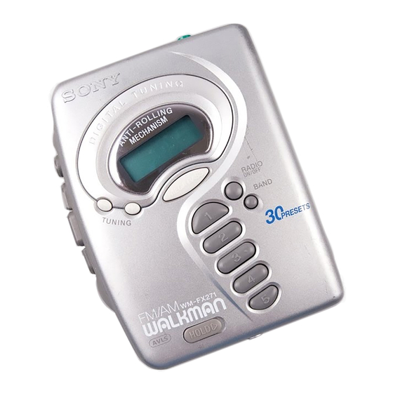
Photo: WM-FX271
× 1
inches) (w/h/d) incl.
5/8
7/16
Model Name Using Similar Mechanism
Tape Transport Mechanism Type
Notes on Chip Component Replacement
• Never reuse a disconnected chip component.
• Notice that the minus side of a tantalum capacitor may be dam-
aged by heat.
Flexible Circuit Board Repairing
• Keep the temperature of the soldering iron around 270˚C during
repairing.
• Do not touch the soldering iron on the same conductor of the
circuit board (within 3 times).
• Be careful not to apply force on the conductor when soldering
or unsoldering.
RADIO CASSETTE PLAYER
– 1 –
US Model
WM-FX271/FX275
Canadian Model
AEP Model
E Model
Chinese Model
WM-FX271
WM-FX171
MF-WMFX171-114
Advertisement
Table of Contents

Related Manuals for Sony WM-FX271


Summary of Contents for Sony WM-FX271
- Page 1 US Model WM-FX271/FX275 Ver 1.0 1999. 02 Canadian Model AEP Model E Model Chinese Model WM-FX271 Photo: WM-FX271 Model Name Using Similar Mechanism WM-FX171 Tape Transport Mechanism Type MF-WMFX171-114 SPECIFICATIONS Frequency range FM: 65 – 74/87.5 – 108 MHz (East European) 87.5 –...
-
Page 2: Table Of Contents
TABLE OF CONTENTS 1. GENERAL ................3 2. DISASSEMBLY 2-1. Cabinet (Front) Sub Assy ............ 4 2-2. Main Board ................. 5 2-3. Holder (Sub) Assy, Cassette ..........5 2-4. Mechanism Deck ..............6 2-5. Belt and Motor ..............6 3. MECHANICAL ADJUSTMENTS ......... -
Page 3: General
SECTION 1 GENERAL This section is extracted from instruction manual. – 3 –... -
Page 4: Disassembly
SECTION 2 DISASSEMBLY • The equipment can be removed using the following procedure. Cabinet (front) sub assy Main board Holder (sub) assy, cassette Belt and Motor Mechanism deck Note : Follow the disassembly procedure in the numerical order given. 2-1. CABINET (FRONT) SUB ASSY Note : When installing, fit the knobs and switches. -
Page 5: Main Board
2-2. MAIN BOARD 3 screw (M1.4), toothed lock (WH) 2 Unsolder the 4 places. 5 MAIN board 1 HEAD FLEXIBLE board (CN301) 4 two claws 2-3. HOLDER (SUB) ASSY, CASSETTE 2 Insert a precision screwdriver (1.4 mm flat-blade) vertically into portion A to release the hinge plate. -
Page 6: Mechanism Deck
2-4. MECHANISM DECK 2 Remove the mechanism deck in the direction of the arrow. 1 Insert the precision screwdriver (1.4 mm flat-blade) into the slit and release three claws. 2-5. BELT AND MOTOR 2 two screws (screw (M1.4), special head) 3 motor •... -
Page 7: Mechanical Adjustments
SECTION 4 SECTION 3 MECHANICAL ADJUSTMENTS ELECTRICAL ADJUSTMENTS PRECAUTION PRECAUTION 1. Clean the following parts with a denatured-alcohol-moistened • Supplied voltage : 2.5V swab : • Switch and control position playback head pinch lever assy VOLUME control : maximum capstan wheel assy rubber belt AVLS switch : NORM... -
Page 8: Tuner Section
TUNER SECTION 0 dB = 1 µV • AM Section Setting: • FM Section RADIO ON/OFF switch: ON Setting: BAND switch : AM RADIO ON/OFF switch: ON BAND switch : FM AM Tuning Voltage Adjustment FM Tuning Voltage Adjustment digital voltmeter digital Main board... - Page 9 Adjustment Location: main board AM IF ADJUSTMENT AM TUNING VOLTAGE ADJUSTMENT AM TRACKING ADJUSTMENT FM TUNING VOLTAGE ADJUSTMENT FM TRACKING ADJUSTMENT Measurement Points: main board (FM RF IN) (VT) FM RF IN – 9 –...
-
Page 10: Diagrams
SECTION 5 DIAGRAMS 5-1. IC PIN DESCRIPTION • IC701 µPD17072GB-559-1A7 (SYSTEM CONTROL/LCD DRIVE) Pin No. Pin Name Pin Description INIT Initialize output 2, 3 — Not used. MEGA BASS MEGA BASS ON/OFF output (L: ON, H: OFF) RADIO-ON Radio circuit power control output 6 –... -
Page 11: Block Diagram
WM-FX271/FX275 5-2. BLOCK DIAGRAM EXCEPT US,CND,C&SA HP901 FM/AM RF, IF, MPX US,CND,C&SA PLAYBACK AUDIO POWER AMP HEAD IC301(1/2) S303-2 FWD IN(L) B.P.F FM IN L OUT REV IN(L) – FM/AM MIX LOCAL R-CH 10.7MHz VOLUME FM IF R OUT R CH ∑... -
Page 12: Printed Wiring Board
WM-FX271/FX275 5-3. PRINTED WIRING BOARD C&SA C&SA • Semiconductor Location Ref. No. Location , C&SA D301 C&SA D302 (FM RF IN) C&SA D303 F-10 D701 F-10 IC301 H-11 IC701 F-11 IC702 F-13 D-10 Q101 H-12 Q201 H-12 Q301 D-10 (VT) -
Page 13: Schematic Diagram
WM-FX271/FX275 5-4. SCHEMATIC DIAGRAM • Refer to page 17 for IC Block Diagrams. (EE) (EXCEPT EE) Note: • All capacitors are in µF unless otherwise noted. • U : B+ Line. • Voltage is dc with respect to ground under •... -
Page 14: Exploded Views
SECTION 6 EXPLODED VIEWS NOTE: • IC Block Diagrams • The mechanical parts with no reference • Color Indication of Appearance Parts • Abbreviation IC1 TA2111F number in the exploded views are not supplied. Example : CND : Canadian model •... -
Page 15: Tape Mechanism Section-1
6-2. TAPE MECHANISM SECTION-1 (MF-WMFX171-114) HP901 M901 Ref. No. Part No. Description Remark Ref. No. Part No. Description Remark 3-013-560-11 BELT X-3369-749-7 PINCH LEVER (N) ASSY 3-703-816-31 SCREW (M1.4), SPECIAL HEAD 3-920-996-01 SPRING (PINCH N) 3-921-042-01 GEAR (REEL) HP901 1-500-532-11 HEAD, MAGNETIC (PLAYBACK) 3-703-816-73 SCREW (M1.4), SPECIAL HEAD M901 1-763-073-11 MOTOR (CAPSTAN/REEL) (including PULLEY) -
Page 16: Tape Mechanism Section-2
6-3. TAPE MECHANISM SECTION-2 (MF-WMFX171-114) Ref. No. Part No. Description Remark Ref. No. Part No. Description Remark 3-921-797-01 WASHER 3-921-335-03 WASHER, LEVER 3-921-003-01 BEARING 3-920-990-01 SPRING (UD), COMPRESSION 3-938-628-01 SPRING (PLAY-CP) 3-921-050-01 GEAR (B) 3-920-999-01 GEAR (A) X-3372-619-2 WHEEL ASSY (NP), CAPSTAN X-3375-837-1 CLUTCH ASSY 3-921-043-01 GEAR (D) 3-013-142-01 SPRING (FR-CP) -
Page 17: Electrical Parts List
SECTION 7 MAIN ELECTRICAL PARTS LIST NOTE: • Due to standardization, replacements in • Items marked “*” are not stocked since When indicating parts by reference the parts list may be different from the they are seldom required for routine service. number, please include the board. - Page 18 MAIN Ref. No. Part No. Description Remark Ref. No. Part No. Description Remark C326 1-164-505-11 CERAMIC CHIP 2.2uF < IC > C327 1-162-964-11 CERAMIC CHIP 0.001uF C332 1-162-974-11 CERAMIC CHIP 0.01uF 8-759-493-20 IC A2111F-(EL) C333 1-126-162-11 ELECT 3.3uF IC301 8-759-574-69 IC LB8115W-TLM C334 1-107-826-11 CERAMIC CHIP 0.1uF...
- Page 19 MAIN Ref. No. Part No. Description Remark Ref. No. Part No. Description Remark Q306 8-729-403-17 TRANSISTOR XN1215 R111 1-216-821-11 METAL CHIP 1/16W Q307 8-729-422-27 TRANSISTOR 2SD601A-Q R112 1-216-821-11 METAL CHIP 1/16W Q308 8-729-900-52 TRANSISTOR DTC114YK R203 1-216-835-11 METAL CHIP 1/16W Q701 8-729-422-27 TRANSISTOR 2SD601A-Q R204...
- Page 20 WM-FX271/FX275 MAIN Ref. No. Part No. Description Remark Ref. No. Part No. Description Remark R708 1-216-833-11 RES,CHIP 1/16W ACCESSORIES & PACKING MATERIALS R709 1-216-833-11 RES,CHIP 1/16W ******************************** R710 1-216-833-11 RES,CHIP 1/16W R711 1-216-833-11 RES,CHIP 1/16W 1-505-521-11 HEADPHONE (MDR-023) R712 1-216-833-11 RES,CHIP...
- Page 23 WM-FX271/FX275 1. PRINTED WIRING BOARD C&SA C&SA • Semiconductor Location Ref. No. Location , C&SA D301 C&SA D302 (FM RF IN) C&SA D303 D701 F-10 IC301 H-11 IC701 F-11 IC702 F-13 D-10 Q101 H-12 Q201 H-12 Q301 D-10 (VT) Q302...
- Page 24 WM-FX271/FX275 2. SCHEMATIC DIAGRAM • Refer to page 2 for Note on Schematic Diagram. – 5 – – 6 –...
- Page 25 MAIN MAIN 3. ELECTRICAL PARTS LIST NOTE: Ref. No. Part No. Description Remark Ref. No. Part No. Description Remark • Due to standardization, replacements in • Items marked “*” are not stocked since When indicating parts by reference C325 1-104-847-11 TANTAL. CHIP 22uF D302 8-719-801-78 DIODE 1SS184...
- Page 26 MAIN Ref. No. Part No. Description Remark Ref. No. Part No. Description Remark Q303 8-729-402-13 TRANSISTOR XN1501 R110 1-216-815-11 METAL CHIP 1/16W Q304 8-729-141-48 TRANSISTOR 2SB624-BV345 (US,CND,2AEP) Q305 8-729-402-13 TRANSISTOR XN1501 R110 1-216-816-11 METAL CHIP 1/16W Q306 8-729-403-17 TRANSISTOR XN1215 (FR) Q307 8-729-422-27 TRANSISTOR 2SD601A-Q...
- Page 27 WM-FX271/FX275 MAIN Ref. No. Part No. Description Remark R701 1-216-837-11 METAL CHIP 1/16W (EXCEPT EE) R701 1-216-842-11 METAL CHIP 1/16W (EE) R702 1-216-839-11 METAL CHIP 1/16W (EXCEPT EE) R702 1-216-845-11 METAL CHIP 100K 1/16W (EE) R703 1-216-812-11 METAL CHIP 1/16W...
Need help?
Do you have a question about the WM-FX271 and is the answer not in the manual?
Questions and answers