Panasonic EB-X400 Service Manual
Personal cellular telephone
Hide thumbs
Also See for EB-X400:
- Operating instructions manual (88 pages) ,
- Operating instructions manual (48 pages)
Table of Contents
Advertisement
Quick Links
This service information is designed for experienced repair technicians only and is not designed for use by the general public.
It does not contain warnings or cautions to advise non-technical individuals of potential dangers in attempting to service a
product.
Products powered by electricity should be serviced or repaired only by experienced professional technicians. Any attempt to
service or repair the product or products dealt with in this service information by anyone else could result in serious injury or
death.
EB-X400
Tx Frequency Range
Rx Frequency Range
Tx / Rx separation
RF Channel Bandwidth 200 kHz
Number of RF channels
Speech coding
Operating temperature -10 C to +55 C
Type
RF Output Power
Modulation
WAP / GPRS
Connection
Voice digitizing
Transmission speed
Signal Reception
Antenna Impedance
(External Connector)
Antenna VSWR
Dimensions
(Excluding antenna)
Volume
Weight
Main Display
Illumination
Keys
SIM
External DC Supply
Voltage
Battery
Standby Time
Talk Time
Talk and standby time will be dependent on network conditions, SIM card, backlight usage and network
condition.
WARNING
R
Personal Cellular Telephone
900 MHz
880 - 915 MHz
925 - 960 MHz
45 MHz
174
Full rate / Half rate / Enhanced Full rate
Class 4 Handheld
2 W maximum
GMSK (BT = 0.3)
WAP 2.0 / GPRS Class 8
8 ch / TDMA
13 kbps RPE-LTP / 13 kps ACLEP / 5.6 kps CELP / VSLEP
270.833 kbps
Direct conversion
50
< 2.1 : 1
Height : 84 mm
Width : 47.4 mm
Depth : 17.5 mm
65 cc
85 g
LCD : 128 x 128 pixels, 65,536 colours
10 LEDs for Keypad Backlighting (White)
4 LEDs for LCD Backlighting (White)
3 LEDs for Sub LCD (Blue, Green, Orange)
16-key Keypad, Navigation key, 1 shutter key
3 V Plug-in type only
5.8 V
3.7 V nominal, 600mAh, Li-Ion
210 hrs
4.5 hrs
2 0 0 4
P a n a s o n i c M o b i l e C o m m u n i c a t i o n s C o . , L t d .
A l l r i g h t s r e s e r v e d . U n a u t h o r i z e d c o p y i n g a n d
d i s t r i b u t i o n i s a v i o l a t i o n o f l a w .
by Toko (toko@gsm-free.org)
1800 MHz
1710 -1785 MHz
1805 -1880 MHz
95 MHz
374
Class 1 Handheld
1 W maximum
Advertisement
Table of Contents

Related Manuals for Panasonic EB-X400


Summary of Contents for Panasonic EB-X400
- Page 1 Toko (toko@gsm-free.org) Personal Cellular Telephone EB-X400 900 MHz 1800 MHz Tx Frequency Range 880 - 915 MHz 1710 -1785 MHz Rx Frequency Range 925 - 960 MHz 1805 -1880 MHz Tx / Rx separation 45 MHz 95 MHz RF Channel Bandwidth 200 kHz...
-
Page 2: Table Of Contents
The information contained in this manual and all rights in any design disclosed therein, are and remain the exclusive property of Panasonic Mobile Communications Co., Ltd. Other patents applying to material contained in this publication:... - Page 3 5.2.8. Audio ................5-16 5.2.9.
- Page 4 9. REPLACEMENT PARTS LIST ..............9-1 9.1.
-
Page 5: Introduction
They must not be incinerated, or disposed of as ordinary rubbish. 1.1. Purpose of the Manual This Service manual contains the information and procedures required for installing, operating and servicing the Panasonic GSM Personal Cellular Mobile Telephone system operating on GSM Digital Cellular Networks. -
Page 6: General Description
2.2. Features The Panasonic Telephone Model EB-X400 is a high performance, small, light, handset for business and domestic use. The following features are provided: Triple Rate, which includes Full Rate, Half rate and Enhanced Full Rate (EFR) speech, codec. -
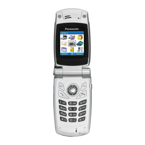
Page 7: Operating Instructions
3. OPERATING INSTRUCTIONS 3.1. General This section provides a brief guide to the operation and facilities available on the telephone handset. Refer to the Operating Instructions supplied with the telephone for full operational information. 3.2. Controls and Indicators Earpiece Main Display One Push Auto Open button Navigation Key Press to open the handset... -
Page 8: Liquid Crystal Display
3.3. Liquid Crystal Display The telephone handset has a graphical chip on glass display. The following icons are available: Main menu screen Figure 3.2: Liquid Crystal Display 3.4. Text Entry (Edit) Alphanumeric characters to enter details into the Phonebook, to create text, email, message, etc. Text Mode ®... -
Page 9: Menu Structure
(SIM Tool Kit) Download Sounds Alarm Settings Shortcuts Sound recorder Text templates Calculator Memory status Infrared Browser Messages Camera PANASONIC BOX Create new Inbox Archive Voicemail (Chat) Cell Broadcast Settings Memory status Settings Profiles Sound Contacts Vibration Alert Contacts list... -
Page 10: Technical Specifications
4. TECHNICAL SPECIFICATIONS 4.1. Tx Characteristics All data is applicable to E-GSM 900 and GSM 1800 except where stated. 4.1.1. Frequency Error 0.1 ppm max., relative to base station frequency. 4.1.2 Modulation Phase Error RMS: Equal to or less than 5 Peak: Equal to or less than 20 4.1.3. -
Page 11: Spurious Emissions At Antenna Connector
4.1.5. Spurious Emissions at Antenna Connector Limits (dBm) Frequency Filter Approx Frequency Range offset Bandwidth Video B/W E-GSM 900 GSM1800 100 kHz to 50 MHz – 10 kHz 30 kHz –36 –36 50 MHz to 500 MHz – 100 kHz 300 kHz –36 –36... - Page 12 E-GSM 900 Half Rate Speech The reference sensitivity performance in terms of frame erasure, bit error, or residual bit error rates (whichever is appropriate) is specified in the following table, according to the propagation conditions. Channels Propagation conditions Propagation conditions Propagation conditions TU high Test Limit...
- Page 13 Blocking: Small MS level in dB Vemf( ) Frequency E-GSM 900 GSM 1800 FR 600 kHz to FR 800 kHz FR 800 kHz to FR 1,6 MHz FR 1,6 MHz to FR 3 MHz 915 MHz to FR - 3 MHz –...
-
Page 14: Technical Description
5. TECHNICAL DESCRIPTION 5.1. RF Overview 5.1.1. RF Block Diagram U101 Transceiver IC FL201 Rx SAW Filter DCS I/IB B7821 DC offset Compensation DCS1800 1805 - 1880 MHz Q/QB FL202 PLLON Rx SAW Filter EGSM B7820 AM_TRIG EGSM900 925 - 960 MHz 3420 - 3980 MHz U301 TCXO module... - Page 15 (RF2V8, VCC_VCXO) are provided for the rest of the RF circuitry from the U2006. Antenna Fixed helical typed antenna is utilised for EB-X400. Its length is 16 mm and located at the top of the lower unit. It covers 900 MHz and 1800 MHz.
-
Page 16: Block Diagrams
5.2.1. Baseband Block Diagram The EB-X400 Baseband is based around a GSM chipset developed by Infineon chip set. The Infineon chipset consists of 2 chips, one is a signal processing chip with DSP and CPU included the analogue baseband (e.g. RF, Audio, SIM), and the other is U2006 (E-Power) which manages power supply and charge control. - Page 17 8 0.4 W speaker amplifier integrated IrDA The IrDA transceiver function is added to EB-X400 to enable wireless data exchange with PCs and other handsets. Real Time Clock (RTC) Time and calendar informations provided within U2001, obviating the need for an external RTC.
- Page 18 The memory interface of the U2001 E-Gold + V3 supports 1.8 V or 2.6 V operation, allowing flexibility on the choice of memory components. EB-X400 adopted 2.6 V operation because the operation voltage of memory is 3.0 V operation.
- Page 19 Clock Interface The U2001 (E-Gold + V3) clock generation unit is used to generate all major system clocks. There are two clock signals connected to the clock generation unit. 8 32 kHz clock F32K 8 26 MHz clock F13/26M The 32 kHz oscillator is used for the Real Time Clock block. As a power-saving feature the 32 kHz clock can be also used for the MCU domain.
- Page 20 Interrupt and Exception Handler An Interrupt and Exception Handler is responsible for managing all system and core exceptions. There are four different kinds of exceptions that are executed in a similar way: 8 Interrupts generated by the Interrupt Controller (ITC) 8 DMA transfers issued by the Peripheral Event Controller (PEC).
- Page 21 The maximum key resistance is 2 k , leakage between any two key matrix lines must be kept below 5 A. The End Key is also used to power on the phone it is allocated a complete ROW of the keyboard scan. EB-X400 supports the VSCL games and keypad assignments for VSCL games refers to the below table. Keypad assignments...
- Page 22 Mbaud and IrDA DS3001 support up to 115.2 kBaud. ASC1 running up to 3.25 Mbaud and with IrDA support up to 115.2 kBaud. EB-X400 uses ASC0 port for serial interface in factory and software download. ASC1 port is used for DS3001 data transmission.
- Page 23 1 - 2 A, hence backup can be provided simply by adding a large capacitance on the RTC supply. In backup mode (E-Gold + powered off) with only the RTC running, the RTC will operate down to app. 1 V. EB-X400 has very large backup capacitors.
- Page 24 Uplink / Downlink I & Q U2001 (E-Gold + V3) performs GMSK modulation on data samples received form DSP at 270 Kbits per second. The I & Q signals are multiplexed to interface with the SMARTi RF IC. Earpiece GSM 900/1800 Automatic Speech Ringer...
- Page 25 The functions of the four external A/D inputs are as follows. E-Gold+ V3 A/D inputs E-Gold + input Pin No. Function Values VBAT Battery voltage TBAT Battery Temperature TENV Environment Temperature TVCO Quartz Temperature No connection in EB-X400 BTEC Battery technology identification No connection in EB-X400 – 5-12 –...
-
Page 26: Cpu Memory
36 Mbits RAM organised as 128k x 32 (Internal SRAM) + 2M x 16 (mobile RAM) EB-X400 uses Dual operation Flash memory + mobile RAM 3-chip stacked type MCP (Multi-Chip Package) to reduce chip mount spaces. 36-Mbit RAM consists of 4-Mbit internal SRAM of E-Gold + V3 and 32-Mbit external mobile RAM on the MCP device. -
Page 27: Main Lcd
These registers are write access only. 5.2.6. IrDA The IrDA module is mounted on the upper unit PCB. EB-X400 supports IrDA file transfer and object exchange, but does not support IrDA dial-up. In a special asynchronous mode of U2001 (E-Gold+ V3), the ASC supports IrDA data transmissions up to 115.2 KBaud with fixed or programmable IrDA pulse width. - Page 28 EB-X400 use the ASC1 port for IrDA interface because serial baud rate of ASC1 is up to 115.2 kbps. This value is satisfies the IrDA requirement. Otherwise, serial baud rate of ASC0 is up to 921.6 kbps. Thus, EB-X400 will use this interface for serial communication in factory and re-programming software.
-
Page 29: Audio
The U2011 features a speaker amplifier for playback synthesized tones though an internal amplifier before application to 8 speaker, and a stereo headset amplifier output. For desktop handsfree applications, the voiceband downlink signal from the U2001 (E-Gold + V3). Series resistors/capacitors adapts the 8 speaker to output drive capability of the U2001, and protects the speaker outputs of the U2001 against the large voltage swing of the U2011 output amplifier. -
Page 30: Power Management
Figure 5.12. GSM Transmit Audio frequency response mask DTHF Speaker To achieve desktop handsfree feature EB-X400 has DTHF speaker mounted on the lower case back. EB-X400 rings some melody tones using DTHF speaker via Melody IC (U2011). This LSI IC can control ringing volume. - Page 31 The headset can be powered externally by Switching-type AC adaptor or DC adaptor. The Switching-type AC adaptor complies with the worldwide voltage regulations. Input Output Voltage Voltage Current AC Adaptor Switching type 100 - 240 V 5.8 V 650 mA Figure 5.13.
- Page 32 60 mV E-Power may be powered up either by a high level on pin ON or by an external supply voltage being applied on pin VDDCH. If the EB-X400 is powered up for the first time after a battery has been inserted the high level on pin ON may only be caused by a power-on push button having been pressed.
-
Page 33: Polytone Ic
9 Power Off Control EB-X400 may be powered down either by a command from E-Gold + V3 or if the battery voltage drops below 2.84 V 60 mV. Usually the RTC regulator will continue operation. The RTC regulator is turned off when the battery voltage has dropped below 2.05 V... -
Page 34: Ui Related Control
When the battery is fitted, EB-X400 charging algorithm is determined by constant voltage and constant current control with time, temperature and voltage safe-guards. A current limit no greater than the maximum charge current for any battery option must be provided by the external power source. - Page 35 The vibrator motor uses discrete components and is controlled by the MCU data bus via the Melody IC (U2011 (EXT2 pin)). The EB-X400 vibrator uses a coin type vibrator to save space on the PCB. 9 UI related Sleep control restrictions When E-Power is set to Sleep mode, the step down converter of E-Power changes the operation mode from PWM to PFM to save battery power.
-
Page 36: Power Consumption
Figure 5.15. UI condition state transition verses System sleep control restrictions 5.2.11. Power Consumption The estimated talk time and standby times for EB-X400 are as follows. This estimated standby time is calculated by using DRX n=9, no neighbour cell, no GPRS condition. -
Page 37: Interface
5.2.12. INTERFACES RF Interface Signals No. Signal Name LOG Function Connection Status Multiplexed I signal QRX of E-Gold + V3 DC center 1.35 V for demodulator (SMARTi) Multiplexed nI signal QR of E-Gold + V3 DC center 1.35 V for demodulator (SMARTi) Multiplexed Q signa IR of E-Gold + V3 DC center 1.35 V for demodulator (SMARTi) - Page 38 Camera Module Interface Signals No. Signal Name LOG Function Connection Status/Description SDATA Pixel clock from camera Companion IC CMCLKIN 6MHz Digital GND Companion IC CMDAT0 Hi-Z at power down. Data Bus (3) Companion IC CMDAT1 Hi-Z at power down. Data Bus (4) Companion IC CMDAT2 Hi-Z at power down.
-
Page 39: External Interface
5.2.13. EXTERNAL INTERFACE No. Signal Name LOG Function H/H Circuit Audio ground 2.2 K 0.1 F HS-TX Sending audio from personal headset 0.1 F HS-RX Received audio to personal headset CC02IO HS_DET Personal headset detection signal E-Gold + V3 CC19IO HOOK_KEY Incoming call/end call signal at personal headset E-Gold + V3... -
Page 40: Disassemby / Reassemby Instructions
6. DISASSEMBLY / REASSEMBLY INSTRUCTIONS 6.1. General This section provides disassembly and reassembly procedures for the main components of the telephone. These assemblies MUST be performed by qualified service personnel at an authorized service center. The following Warnings and Cautions MUST be observed during all disassembly / reassembly operations: WARNING The equipment described in this manual contains polarized capacitors utilizing liquid electrolyte. -
Page 41: Disassemby
6.2. Disassembly 6.2.1. Lower Case Assembly and Main PCB Removal Place thumbs at outer edges of battery cover, press down, then slide the battery cover towards the bottom of the phone. Lift and remove battery. Using tweezers, remove the two grey screw caps. Discard these items. -
Page 42: Upper Case Assembly And Display Module Removal
Disconnect the SIM connector board A from the Main PCB. Disconnect the board to board connector B from the Main board. 6.2.2. Upper Case Assemby and Display Module Removal Open the phone. Using tweezers or a pin, remove the two grey screws cap and discard. Remove the logo panel and discard. - Page 43 Insert the plastic strip (of gutar pick thickness) into the top of the upper case to unhook the hook. Caution: Do not insert the separation tool at side plate area. Open the upper case with finger and then insert the separation tool (of gutar pick thichness) into deeply the gap of the upper case and then slide direction of the arrow.
-
Page 44: Removal Of Hinge Unit And Spigot
Disconnect the main LCD flexi-strip A and camera flexi-strips B. Unhook C and D then remove the LCD board. 6.2.3. Removal of Hinge Unit and Spigot Set the phone into the "open " position. Remove the hinge stopper from the lower front cover. Using a small screwdriver blade or blunt instrument, apply pressure to the one push hinge direction while pulling the hinge away from the case. -
Page 45: Antenna Removal
Take care not to damage the board-to-board flexi-strip. 6.2.4. Antenna Removal It is only necessary to remove the antenna if the antenna contact is damaged. Using a small screwdriver blade or blunt instrument. Apply pressure to the antenna lug in direction shown while pulling the anntenna away from the case. -
Page 46: Hinge Reassembly
6.3. Reassembly 6.3.1. Hinge reassembly Insert the board-to-board flexi-strip into the slot of the hinge guide. Fit the slot of the upper front cover to the board-to-board flexi-strip. Twist the lower case unit until both sides of the hinge locate inside the case. –... - Page 47 Set the phone into the" Open" position. Insert the one push hinge A into the upper case assembly. Locate the LCD assembly onto the upper front cover Connect the board-to-board connector and reciever/speaker flexi-strip on the upper PCB. – 6-8 –...
-
Page 48: Repair Procedures
7. REPAIR PROCEDURES 7.1. Introduction This section provides information on testing the telephone. The layout is as follows: Section 7.2. : Lead Free (PbF) solder: Identification and repair of PCBs using PbF solder. Section 7.3. : External testing: describes equipment requirements and general set up procedure. Section 7.4. - Page 49 PCB Repair Jig (Part No. 3WZ001139AAA) The PCB Repair Jig provides the necessary connections between the PCB Assembly and external test equipment. It is required for RF calibration. Figure 7.1. : PCB Repair Jig A cable with SMA female connector is provided to make the RF connection. An SMA to N-Type male adaptor will be required to connect the Repair Jig to the service equipment.
- Page 50 Power Cable (Part No. 3WZ001130AAA) The power cable provides the necessary connections between the PCBA repair jig / dummy battery and external power supply. Figure 7.3. : Power Cable Data Cable (Part No. 3WZ001107AAA) The data cable for used to software download and calibration. Figure 7.4.
-
Page 51: Software Download & Adjustment Procedures
8. SOFTWARE DOWNLOAD & ADJUSTMENT PROCEDURES 8.1. FlashTool update and operation guide 8.1.1. Introduction The system has been tested on the following platforms: Win98, Win2000, WinXP System overview PC(with "Dongle") Phone serial port Headset Jack Stabilized Power Supply voltage : 3.8 V NOTE : If using a battery pack to power the phone, ensure that it is fully charged. -
Page 52: Software Upgrade Procedure - Flashtool Operation By Using Spk File
8.3. Software upgrade procedure - FlashTool operation by using SPK file Select [Start]-[Program]-[FlashTool]-[FlashTool_4_4] in PC menu. Then the following screen appears. Click the tab of "Use SPK file". Click the tab of "Use SPK file". 8.3.1. Select SPK file The following screen is displayed. Click "None"... - Page 53 The following screen is displayed. Move to the folder where .dffs is located Select .spk file and press "Open" button. Then the path and name of .spk file are displayed. Then Click "OK". Check that all required files are in the same folder. –...
-
Page 54: Com Port Set-Up
8.3.2. COM port set-up The following screen is displayed. Each item can be changed by clicking the blue part. First COM port: Specify port number to connect the data cable. Number of COM ports: Number of actual machines to write. Normally one machine at a time, so 1 will be OK. Baud rate: When COM port is used on PC, enter 115200. -
Page 55: Start Download
The download procedure is as follows: 1. Ensure that a fully charged battery is connected to the phone. 2. Connect the EB-X400 to the PC via the data cable. This is the download screen. Click around "Click to start". - Page 56 When download starts, progress bar is displayed. Please do not disconnect the data cable while downloading. When download is successful, the following screen is displayed. – 8-6 –...
- Page 57 In case of an error, the following screen is displayed. If a download fails, check all connections between the phone, data cable and PC. Before restarting the download procedure, remove and then re-attach the phone battery. – 8-7 –...
-
Page 58: Rf Calibration
8.4. Baseband and RF Calibration 8.4.1. System Overview Power Meter Signal Generator PC (with "Dongle") Phone Headset Jack Stabilised Power Supply Voltage : 3.7 V Cable 8.4.2. P-test Mode Press the power key to turn on the mobile phone. Start the PhoneTool program. The following screen is then displayed: 1. -
Page 59: Battery Voltage Ad Calibration
NOTE : If the message "ERROR! No Connection" is displayed, check the cable connections, the power supply and that the phone is switched on. Repeat steps 1 and 2. 3. Select "ptest_mode", and check the log window. >>> "Sending to mobile...OK". The mobile is now in ptest_mode. - Page 60 1. Click the "Non signaling mode" button. 2. Click Connection button. 3. Check the ADC Meas(urement). 4. Change the power supply PS-1 voltage from 3.7 V to 4.0 V 5. Check the vbat = 4.0 V value. If vbat = 4.0 V is outside the range -7000 to +6000, then the unit has failed. 6.
-
Page 61: Battery Temperature Ad Calibration
8.4.5. Battery Temperature AD Calibration 1. Supply the TBAT = 2.0v by PS-2. 2. Check the tbat = 2.0 V value If the value is outside the range -20000 to -900, then the unit has failed. 3. Enter the calibrated tvat = 2.0 V value to the Excel sheet. 4. - Page 62 8.4.6. Transmit Power Calibration Note: To calibrate the mobile, set it to ptest_mode. Click modes button and select "Non signaling test". 1. Click the "Non signaling mode" button. 2. Click the Check Connection button. 3. Select TSC = 5. 4. Check "Enable/Disable Editor". 5.
- Page 63 Power Level Calibration Before starting Power Level Calibration, the Power Ramp Editor should be enabled. The mobile should be connected to GSM Tester or Power Meter. 1. Select the required Band and PA Level, and click the "Get" button. The default ramping value for the selected band and PA Level will be displayed. 2.
- Page 64 4. Input an appropriate value for "Up Ramp 16", and click "set". Check that the power meter registers a change in power level. 5. Repeat step 4 (Input and set) until the target power level is displayed on the power meter. (Refer to the Calibration Specification table below.) Calibrating Specification Table Note that each frequency band is divided into segments and that each segment has a Calibration Channel allocated to it.
- Page 65 E-GSM900 Output (dBm) Power Level Terget (PL) Nominal 31.75 31.5 32.0 30.4 30.0 30.9 28.5 28.5 29.5 26.5 26.5 27.5 24.5 24.5 25.5 22.5 22.5 23.5 20.5 20.5 21.5 18.5 18.5 19.5 16.5 16.5 17.5 14.5 14.5 15.5 12.5 12.5 13.5 10.5 10.5...
- Page 66 6. Enter the calibrated Ramping value into the following TX Excel sheet. The Ramping value will be automatically calculated to the pa_offset value and then stored to the eep file of the Excel sheet. 7. To calibrate other PA Levels or Bands, repeat steps 1 to 6. After finished all calibrate the Ramping value and then it input to following Excel sheet.
-
Page 67: Rxlev Calibration
Rename the Text file from the original filename and then save to PC. 8.4.7. Rxlev Calibration NOTE: To calibrate Rxlev, the mobile should in under ptest_mode. Rxlev gain calibration The mobile should be connected to the Signal Generator. RF input level is –90 dBm. Select "Non signaling mode"... - Page 68 1. Select the Gain "Rx(1) = 70 dB". 2. Check the "Burst Rx" of the RF Mode. 3. Input the Rx ARFCN (EGSM = 37 ch, DCS = 670 ch) and press the Enter key. 4. Click the "Get" button of Rx IQRMS. The value displayed at "Slot1"...
-
Page 69: Data Overwrite Procedure
7. Rename the txt file from the original filename and then save to PC. 8.4.8. Data Overwrite Procedure Press the power key to turn on the mobile phone. Start the Phone Tool program. Click the "V24 At# On". Click the Check Connection button. When the log window displays the message "Connection OK", select "EEPROM". - Page 70 1. Click "Edit à Setting" , and check "Read static EEPROM value only from phone". 2. Click "Read EEPROM value from phone". The "eep-static" folder is opened. 3. Click "Load Eeprom Text File". 4. Select "Any File" of the Files of type 5.
-
Page 71: Normal Mode
7. Click "Download current Eeprom values to phone". 8. Click "OVERWRITE" button. The TX, RX and Battery calibration values in the phone will be overwritten by the new values from the PC. 8.4.9. Normal Mode NOTE: When calibration has been completed, the mobile should be set to normal_mode. Press the power key to turn on the mobile phone. -
Page 72: Replacement Parts List
9. REPLACEMENT PARTS LIST 9.1. Case and Cover Parts List M103 M110 M211 M231 M201 M129 M102 M204 M214 M114 M208 M216 M105 M232 M236 M112 M206 M210 M213 M218 M205 M223 M202 M224 M233 M108 M128 M220 M111 M219 M221 M217 M207... - Page 73 REF. NO. PART NO. DESCRIPTION REF. NO. PART NO. DESCRIPTION M206 3DB001085AAA HSJ CAP (BLACK) EBX400-E5 MOUNTED UPPER PCB 3DB001085AAB HSJ CAP (WHITE) B3RBC0000023 IRDA 3DB001085AAC HSJ CAP (RED) K1MN21B00052 LCD CONNECTOR M207 3CH001272AAA SIM PCB HOLDER K1KB24A00043 B TO B CONNECTOR L0ZZ00000017 SPEAKER-RECEIVER ASSY M208...
-
Page 74: Main Pcb Assembly
9.2. Main PCB Assembly Ref. No. Part No. Part Name & Description Grid Ref. No. Part No. Part Name & Description Grid BT2001 N4EZA14A0001 BATTERY G C2009 F1G1A104A012 CERAMIC CAPACITOR 0.1UF 10V C101 F1G1H270A409 CERAMIC CAPACITOR 27PF 50V C2015 F1G1A104A012 CERAMIC CAPACITOR 0.1UF 10V C103... - Page 75 Ref. No. Part No. Part Name & Description Grid Ref. No. Part No. Part Name & Description Grid C2142 F1G1H330A409 CERAMIC CAPACITOR 33PF 50V L102 ELJRF33NJF2 SURFACE MOUNT FIXED COIL 33NH C2143 ECJ0EB0J105K CERAMIC CAPACITOR 1UF 6.3V L103 ELJRF3N3DF2 RF COIL 3.3NH 5.5GHz C2146 F1G1A104A012...
- Page 76 Ref. No. Part No. Part Name & Description Grid Ref. No. Part No. Part Name & Description Grid R2027 ERJ2GEJ473X FIXED RESISTOR 47K 1/16W U101 C1CB00001525 RF TRANSCEIVER IC PMB6256V R2028 ERJ2RKF1543X SPECIAL FIXED RESISTOR 154K 1/16W U102 C1CB00001476 RAMPING CONTROL IC PMB2256V R2029 ERJ2GEJ223X FIXED RESISTOR...
-
Page 77: Upper Face Pcb Assembly
9.3. Upper Face PCB Assembly Ref. No. Part No. Part Name & Description Grid Ref. No. Part No. Part Name & Description Grid C3001 F1G1A104A012 CERAMIC CAPACITOR 0.1UF 10V L3006 G1C4R7MA0104 SURFACE MOUNT FIXED COIL 4.7UH C3002 F1G1A104A012 CERAMIC CAPACITOR 0.1UF 10V Q3001 UNR321N00L... -
Page 78: Hinge Pcb Assembly
9.4. Hinge PCB Assembly 9.5. SIM PCB Assembly Ref. No. Part No. Part Name & Description Grid Ref. No. Part No. Part Name & Description Grid C4002 ECJ0EB1A104K CERAMIC CAPACITOR 0.1UF 10V CN4001 200403110015 SQUARE CONNECTOR CN4002 K1KB02B00014 CONNECTOR CN4003 200402100011 SQUARE CONNECTOR(J) D4001... -
Page 79: Block Diagram
10. BLOCK DIAGRAM 10.1. Baseband VSSPW VANA VINT V3V VRTC VRF1 VRF2 VRF3 U2006 (E-Power) I2C bus SDBB LINT LANA LRF1 Control Charge Control Interface (Step-down) LSIM LRF2 Reference LRTC LRF3 uCapacitor VSIM I2C Bus U2001 (E-GOLD+ V3) Viterbi RF Block GMSK DSP Serial Comm.Interface/... -
Page 80: Rf Band
10.2. RF Band U101 Transceiver IC PMB6256V V1.1 FL201 Rx SAW Filter DCS I/IB B7821 DC offset Compensation DCS1800 1805 - 1880 MHz Q/QB FL202 Rx SAW Filter EGSM PLLON B7820 AM_TRIG EGSM900 925 - 960 MHz 3420 - 3980 MHz U301 TCXO module RF Synth... -
Page 81: Circuit Diagrams
11. CIRCUIT DIAGRAMS 11.1. Main PCB (Baseband) CN2006 FL2001 Memory 51338-0604 MEA2010LC220T002 DATA[0 - 15] OUT4 GND-5 DATA[3] U2008 OUT3 MC-26426312F9-E80X-CR2 DATA[2] ADR[0 - 22], MODE OUT2 ROM/RAM DATA[1] OUT1 TP2038 128MF (16M X 2)/32MS DATA[0] VINT GND-10 FL2002 RY[/BY] /WP[ACC] MEA2010LC220T002 DATA[7]... - Page 82 11.2. Main PCB (RF Band) RF2V8 RF2V8 VCC VCXO RT101 TEMP C301 RF2V8 NCP15WD683J03RC RF2V8 C302 2.2u 26MHz (Baseband) RF IC C351 100p U101 BM BB PMB6256V V1.1 R102 Charge 3-wire-bus Pump Sequencer Voltage RX3CTR Logic Reg. 3.6 GHz ANT Switch DCS SAW Filter VCCVCO RX3X...
- Page 83 Interface 11.3. Upper Face PCB CN3002 FF0221SA1-R3000 LCD IF Companion IC Main Upper Interface R3006 LD[0] LD[7] U3001 LD[2] CN3003 S1D13713B00B10L R3007 COMPANION IC DF30EB-60DS-0.4V(59) LD[3] LD[4] CAM32K R3008 CAM 32K CLKI LD[1] CAM A1 CAM A1 RESET R3043 LD[6] R3009 RESET RESET#...
- Page 84 11.4. Hinge PCB CN5002 CN5001 DF30FB-60DP-0.4V(59) 55909-0604 DATA[0] DATA[1] DATA[2] DATA[3] DATA[4] DATA[5] DATA[6] DATA[7] HCS APPX CAM A[1] HCS LCDX CAM INT RESET AM32K SDIR RXIR TXIR TRI R TRI G TRI B DISP RST TOPLED1 VCHG CUR EN RECN RECP SPOUT1...
- Page 85 11.5. SIM PCB SIM CN VSIM CN4003 BM05106-L2 CCVCC CCRST CCCLK CCIO SIM CN CN4001 DF12B(3.0)-14DP-0.5V(80) VSIM VLOG SIM RST Vibrator SIM CLK Interface VLOG CN4002 SM02B-SURS-TF (LF) SIM IO TP4002 TP4001 R4001 2.7K VIB ON Q4001 2SD2114KT146 VIB CN –...
-
Page 86: Layout Diagrams
12 LAYOUT DIAGRAMS 12.1 Main Board U2001 12 – 1... - Page 87 12 – 2...
- Page 88 12.2. Upper Face PCB Black Green Black White – 12-3 –...
- Page 89 12.3. Hinge PCB – 12-4 –...
- Page 90 12.4. SIM PCB – 12-5 –...
Need help?
Do you have a question about the EB-X400 and is the answer not in the manual?
Questions and answers