
Related Manuals for Protech Systems PPC-7400


Summary of Contents for Protech Systems PPC-7400
- Page 1 USER’S MANUAL PPC-7400 PPC-7402 PPC-7405 PPC-7407 Socket 478 (P4/P4-M) 17”/15”/12.1” Panel PC System PPC-740X M2...
- Page 2 Copyright Notice PPC-740X Panel PC System With LCD / Touch screen (optional) OPERATION MANUAL COPYRIGHT NOTICE This operation manual is meant to assist users in installing and setting up the system. The information contained in this document is subject to change without prior any notice.
-
Page 3: Fcc Notice
Copyright Notice FCC NOTICE This equipment has been tested and found to comply with the limits for a Class A digital device, pursuant to part 15 of the FCC Rules. These limits are designed to provide reasonable protection against harmful interference when the equipment is operated in a commercial environment. -
Page 4: Table Of Contents
Contents TABLE OF CONTENTS CHAPTER 1 INTRODUCTION About This Manual ............Case Illustration ............. System Specification ............. Safety Precautions ............1-12 CHAPTER 2 SYSTEM CONFIGURATION Jumper & Connector Quick Reference Table ....Component Locations ........... How to Set the Jumpers ..........COM Port Connector …………………………………... - Page 5 Contents 2-31 System FAN Connector ……………………………….. 2-31 2-32 North Chip FAN Connector …………………………… 2-31 2-33 Power LED Connector ………………………………… 2-32 2-34 Memory Installation ....………......2-32 2-35 P4/ P4-M CPU Selection ……………………………… 2-33 2-36 Digital Input/Output Connector ……………………….. 2-34 2-37 ATX +12V Power Connector …………………………. 2-34 2-38 LVDS Panel Resolution Selection ……………………..
- Page 6 Contents APPENDIX A SYSTEM ASSEMBLY Exploded Diagram for Removing Arm Holder ……………… Exploded Diagram for Removing Hook Holder ……………… Exploded Diagram for Removing EXT-Case ………………… Exploded Diagram for Removing Back Cover ……………….. Exploded Diagram for Removing LCD Assembly …………. Exploded Diagram for Front Panel …………………………… Exploded Diagram for Removing CD-ROM Assembly ………...
-
Page 7: Chapter 1 Introduction
CHAPTER INTRODUCTION This chapter gives you the information for PPC-740X. It also outlines the System specifications. Section includes: About This Manual Case Illustration System Specifications Safety precautions Experienced users can skip to chapter 2 on page 2-1 for a Quick Start. Page:1-1... -
Page 8: About This Manual
1-1. ABOUT THIS MANUAL Thank you for purchasing our Panel PC. It is an updated system designed to be comparable with the highest performance of IBM AT personal computers. It provides faster processing speed, greater expandability, and can handle more tasks. -
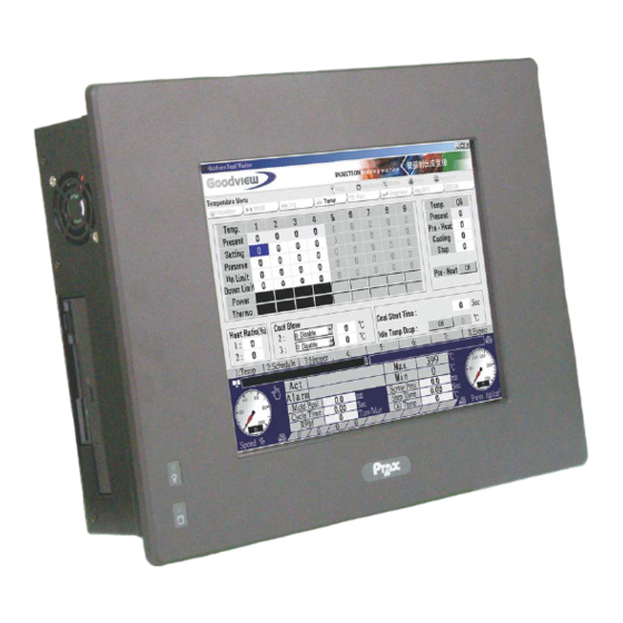
Page 9: Case Illustration
Chapter 1 Introduction 1-2. CASE ILLUSTRATION Page: 1-3 PPC-740X USER S MANUAL... - Page 10 Chapter 1 Introduction Page: 1-4 PPC-740X USER S MANUAL...
- Page 11 Chapter 1 Introduction Page: 1-5 PPC-740X USER S MANUAL...
-
Page 12: System Specification
Chapter 1 Introduction 1-3. SYSTEM SPECIFICATIONS MAINBOARD (PROX-7400) CPU TYPE: Intel® Pentium® 4/Pentium® 4-M/Intel® Celeron/ Mobile processors CPU Frequency 2.0~2.8GHz Auto detect voltage regulator. CHIPSET: Intel® 845GV MEMORY : Up to 1GB DDR SDRAM One 184-pin DIMM sockets on board. CACHE : Built-in CPU(128/256KB Cache). - Page 13 Chapter 1 Introduction SSD SOCKET (OPTIONAL) : One 32-pin socket. Supports Disk-on-chip up to 576MB. BUS SUPPORT : External PCI Bus (Riser card support 1P1I/3P3I). VGA : Integrated in 845GV, supports CRT & TFT-LCD panel. LCD panel connector on board for LVDS panel (7305), 15-Pin VGA D-sub connector on rear panel.
- Page 14 Chapter 1 Introduction COM1/2/3/4 contain 5V or 12V power capability with 9-pin D-sub connector on rear panel. COM4 with 9-pin box-header available for touch panel installed. PARALLEL PORT : One 25-pin D-Sub connector on rear panel. Support for SPP, ECP, EPP Function. Bi-directional parallel port.
- Page 15 Chapter 1 Introduction INTERRUPT LEVELS : LCD PANEL TFT color LCD is manufactured by using very high brightness technology. Some sequential pixels may not light or may light always, but this is not a failure. LCD TYPE : LCD Panel 12.1”: Priority source - Mitsubishi (1 LVDS) or similar model. LCD Panel 15”...
-
Page 16: General Information
Chapter 1 Introduction According to the supplier’s LCD specification. DIMENSION : According to the supplier’s LCD specification. TOUCH SCREEN : (OPTIONAL) Liyi Fuji Vendor Type Resistive Static Load 500g (30 , 30 Sec) Hardness Transparency Write Life 10,000,000 Times 1,000,000 Words Knock Life 35,000,000 Times 10,000,000 Times... - Page 17 Chapter 1 Introduction Output Requirements: (1) +3.3V & +5V total output shall not exceed 70W, and the total output for this subject power supply is 200W. (2) All outputs shall be safety-isolated from the AC mains and share a common return. This common return must be connected to supply chassis.
-
Page 18: Safety Precautions
Chapter 1 Introduction 1-4. SAFETY PRECAUTIONS Following messages are safety reminders on how to protect your systems from damages. And thus, helps you lengthen the life cycle of the system. 1. Check the Line Voltage a. The operating voltage for the power supply should cover the range of 100VAC-240VAC, otherwise the system may be damaged. -
Page 19: Chapter 2 System Configuration
CHAPTER SYSTEM CONFIGURATION Helpful information that describes the jumper & connector settings, and component locations. Section includes: Jumper & Connector Quick Reference Table Component Locations Configuration and Jumper settings Connector Pin Assignments Page 2-1... -
Page 20: Jumper & Connector Quick Reference Table
Chapter 2 Hardware Configuration 2-1. JUMPER & CONNECTOR QUICK REFERENCE TABLE COM Port Connector ……………………………………..COM1, COM2 ……………………………………… COM3, COM4 COM Port RI & Voltage Selection ……………………… RS232/422/485 (COM2) Selection .....…………. VGA Connector …………………………………………… VGA1 LVDS Connector ..........………….. LVDS1, LVDS2 Brightness Voltage Selection ……………………..…….. -
Page 21: Component Locations
Chapter 2 Hardware Configuration 2-2. COMPONENT LOCATIONS PPC-740X Connector, Jumper and Component locations ’ Page: 2-3 PPC-740X USER S MANUAL... -
Page 22: How To Set The Jumpers
Chapter 2 Hardware Configuration 2-3. HOW TO SET THE JUMPERS You can configure your board by setting the jumpers. Jumper is consists of two or three metal pins with a plastic base mounted on the card, and by using a small plastic "cap", Also known as the jumper cap (with a metal contact inside), you are able to connect the pins. - Page 23 Chapter 2 Hardware Configuration JUMPER DIAGRAMS JUMPER SETTINGS ’ Page: 2-5 PPC-740X USER S MANUAL...
-
Page 24: Com Port Connector
Chapter 2 Hardware Configuration 2-4. COM PORT CONNECTOR There are four COM ports enhanced in this board namely: COM1, COM2, COM3 and COM4. COM1, COM3 and COM4 are fixed for RS-232, while COM2 is selectable for RS-232/422/485. COM1 : COM1 Connector The COM1 Connector assignments are as follows : ASSIGNMENT NDCDA... - Page 25 Chapter 2 Hardware Configuration COM3 : COM3 Connector The pin assignments are as follows : ASSIGNMENT NDCDC NSINC NSOUTC NDTRC NDSRC NRTSC NCTSC RIN3 COM4 : COM4 Connector The pin assignments are as follows : ASSIGNMENT NDCDD NSIND NSOUTD NDTRD NDSRD NRTSD NCTSD...
-
Page 26: Com Port Ri & Voltage Selection
Chapter 2 Hardware Configuration 2-5. COM PORT RI & VOLTAGE SELECTION JP8 : COM1, COM2, COM3, and COM4 RI & Voltage Selection The selections are as follows: JUMPER SETTING JUMPER SELECTION (Pin Closed) ILLUSTRATION 13-14 COM1 (Max. 1A) Page: 2-8 ’... - Page 27 Chapter 2 Hardware Configuration 15-16 COM2 (Max. 1A) ’ Page: 2-9 PPC-740X USER S MANUAL...
- Page 28 Chapter 2 Hardware Configuration 17-18 COM3 (Max. 1A) 9-11 Page: 2-10 ’ PPC-740X USER S MANUAL...
- Page 29 Chapter 2 Hardware Configuration 19-20 COM4 8-10 (Max. 1A) 10-12 ’ Page: 2-11 PPC-740X USER S MANUAL...
-
Page 30: Rs232/422/485 (Com2) Selection
Chapter 2 Hardware Configuration 2-6. RS232/422/485 (COM2) SELECTION JP9 : RS-232/422/485 (COM2) Selection COM2 is selectable for RS-232, 422, 485 function. The jumper settings are as follows : COM 2 JUMPER SETTING JUMPER ILLUSTRATION FUNCTION (pin closed) RS-232 Open 1-2, 5-6, 7-8, 9-10 11-12, 13-14, 15-16 RS-422 17-18, 19-20... -
Page 31: Vga Connector
Chapter 2 Hardware Configuration 2-7. VGA CONNECTOR VGA : VGA Connector The pin assignments are as follows: ASSIGNMENT VGA_RED VGA_GREEN VGA_BLUE VCC (Max. 1A) VGA_VDDA VGA_HSYNC_5V VGA_VSYNC_5V VGA_VDDCLK ’ Page: 2-13 PPC-740X USER S MANUAL... -
Page 32: Lvds Connector
Chapter 2 Hardware Configuration 2-8. LVDS CONNECTOR LVDS1 : LVDS Connector The pin assignments are as follows : ASSIGNMEN ASSIGNMENT JCKL1M JA2P JA3P JA0P JA2M JA3M JA0M LPVDD JA1P LPVDD JCLK1P JA1M LVDS2 : LVDS Connector The pin assignments are as follows : ASSIGNMEN ASSIGNMENT JCLK2M... -
Page 33: Brightness Voltage Selection
Chapter 2 Hardware Configuration 2-9. BRIGHTNESS VOLTAGE SELECTION JP11 : Brightness Voltage Selection The selections are as follows : JUMPER SETTING JUMPER SELECTION (Pin Closed) ILLUSTRATION 2.5V ***Manufacturing Default is set as 5V. ’ Page: 2-15 PPC-740X USER S MANUAL... -
Page 34: Lcd Panel Voltage Selection
Chapter 2 Hardware Configuration 2-10. LCD PANEL VOLTAGE SELECTION JP3: LCD Panel Voltage Selection The selections are as follows : JUMPER SETTING JUMPER SELECTION (Pin Closed) ILLUSTRATION 3.3V Page: 2-16 ’ PPC-740X USER S MANUAL... -
Page 35: Power Connector
Chapter 2 Hardware Configuration 2-11. POWER CONNECTOR ATX1: Power Connector The pin assignments are as follows : ASSIGNMENT VCC3_3 VCC3_3 5VSB VCC12 VCC3_3 VCC12J PS_ON VCC5J ’ Page: 2-17 PPC-740X USER S MANUAL... -
Page 36: Floppy Disk Drive Connector
Chapter 2 Hardware Configuration 2-12. FLOPPY DISK DRIVE CONNECTOR FDD1 : Floppy Disk Drive Connector The pin assignments are as follows: ASSIGNMENT ASSIGNMENT INDEXJ DSAJ DSKCHGJ MOAJ DIRJ RWCJ STEPJ TRAK0J RDATAJ HEADJ Page: 2-18 ’ PPC-740X USER S MANUAL... -
Page 37: Hard Disk Drive Connector
Chapter 2 Hardware Configuration 2-13. HARD DISK DRIVE CONNECTOR IDE1 : Hard Disk Drive Connector The pin assignments are as follows: ASSIGNMENT ASSIGNMENT IDERSTJ PDD7 PDD8 PDD6 PDD9 PDD5 PDD10 PDD4 PDD11 PDD3 PDD12 PDD2 PDD13 PDD1 PDD14 PDD0 PDD15 SDREQ SDIOWJ SDIORJ... - Page 38 Chapter 2 Hardware Configuration IDE2 : Hard Disk Drive Connector The pin assignments are as follows: ASSIGNMENT ASSIGNMENT IDERSTJ SDD7 SDD8 SDD6 SDD5 SDD10 SDD4 SDD11 SDD3 SDD12 SDD2 SDD13 SDD1 SDD14 SDD0 SDD15 SDREQJ SIOWJ SIORJ SDIORJ PULL LOW SDDACKJ IRQ15S SDA1...
-
Page 39: Printer Connector
Chapter 2 Hardware Configuration 2-14. PRINTER CONNECTOR LPT1 : Printer Connector As to link the Printer to the card, you need a cable to connect both DB25 connector and parallel port. The pin assignments are as follows : LPT1 ASSIGNMENT ASSIGNMENT STBJR AFDJ... -
Page 40: Lan Connector
Chapter 2 Hardware Configuration 2-15. LAN CONNECTOR LAN1: LAN Connector. The pin assignment is as follows : ASSIGNMENT TXD0P TXD0N TXD1P TXD2P TXD2N TXD1N TXD3P TXD3N 2-16. LAN LED CONNECTOR LANLED1 : LAN LED Connector The pin assignment is as follows : ASSIGNMENT SPEED100J SPEED1000J... -
Page 41: Keyboard Connector
Chapter 2 Hardware Configuration 2-17. KEYBOARD CONNECTOR KB1 : PC/AT Keyboard Connector The pin assignments are as follows : ASSIGNMENT KB DATA KB CLK 2-18. PS/2 MOUSE CONNECTOR MS1 : PS/2 Mouse Connector The pin assignments are as follows : ASSIGNMENT MS DATA MS CLK... -
Page 42: Sound Connector
Chapter 2 Hardware Configuration 2-19. SOUND CONNECTOR The sound connector is composed of the Microphone (MIC1), Line-Out (LINE_OUT), Line-In (LINE_IN) and CDIN connector. LINE IN : Line-In Connector The pin assignment is as follows : ASSIGNMENT LINE_L LINE_R MIC1 : Microphone Connector The pin assignment is as follows : ASSIGNMENT MIC-IN... -
Page 43: Reset Connector
Chapter 2 Hardware Configuration CDIN1 : CDIN Connector The pin assignment is as follows : ASSIGNMENT CD-L CDGND CDGND CD-R 2-20. RESET CONNECTOR JP10 (9-10) : Reset Connector. The pin assignment is as follows : ASSIGNMENT RSTSW 2-21. HDD LED CONNECTOR HDLED1 : HDD LED Connector The pin assignment is as follows : ASSIGNMENT... -
Page 44: Power Button
Chapter 2 Hardware Configuration 2-22. POWER BUTTON PWBN : Power Button The pin assignments are as follows: ASSIGNMENT PW_BN1 PANSWIN 2-23. EXTERNAL SMI CONNECTOR JP10 (5,7) : External SMI Connector. The pin assignments are as follows : ASSIGNMENT P_ESMI 2-24. EXTERNAL SPEAKER CONNECTOR JP10 (2, 4, 6, 8) : External Speaker Connector. -
Page 45: Keylock Connector
Chapter 2 Hardware Configuration 2-25. KEYLOCK CONNECTOR JP10 (1, 3) : Keylock Connector. The pin assignments are as follows : ASSIGNMENT KEYLOCKJ 2-26. CMOS FUNCTION SELECTION JP4: CMOS Function Selection The selections are as follows: JUMPER SETTING JUMPER FUNCTION ILLUSTRATION (pin closed) NORMAL CLEAR CMOS... -
Page 46: Universal Serial Bus Connector
Chapter 2 Hardware Configuration 2-27. UNIVERSAL SERIAL BUS CONNECTOR USB1: Universal Serial Bus Connector. The pin assignments are as follows : ASSIGNMENT USBV0 (Max. 500mA) USBP0N USBP0P USB2: Universal Serial Bus Connector. The pin assignments are as follows : ASSIGNMENT USBV1 (Max. -
Page 47: Usb Connector
Chapter 2 Hardware Configuration USB4 : Universal Serial Bus Connector. The USB connector is reserved for touch panel. The pin assignments are as follows : ASSIGNMENT USBV3 USBP3N USBP3P 2-28. INVERTER CONNECTOR CN2 : Inverter Connector The pin assignments are as follows: ASSIGNMENT V12SAFE BRCRT... -
Page 48: Reset/Nmi/Clear Watchdog Selection
Chapter 2 Hardware Configuration 2-29. RESET / NMI /CLEAR WATCHDOG SELECTION JP6 : Reset/NMI/Clear Watchdog Selection The selections are as follows: JUMPER FUNCTION JUMPER SETTING ILLUSTRATION Reset Watchdog *** Manufacturing Default --- is set as Reset. User may select to use the Reset or NMI watchdog. NMI, also known as Non-Maskable Interrupt, is used for serious conditions that demand the processor’s immediate attention, it cannot be ignored by the system unless it is shut off specifically. -
Page 49: Cpu Fan Connector
Chapter 2 Hardware Configuration 2-30. CPU FAN CONNECTOR CPUFAN : CPU Fan Connector The pin assignments are as follows : ASSIGNMENT VCC12 (Max. 1A) FANIO1 2-31. SYSTEM FAN CONNECTOR SYSFAN : System Fan Connector The pin assignments are as follows : ASSIGNMENT VCC12 (Max. -
Page 50: Power Led Connector
Chapter 2 Hardware Configuration 2-33. POWER LED CONNECTOR PWLED1: Power LED Connector. The pin assignments are as follows : ASSIGNMENT PW_LED+ PW_LED- 2-34. MEMORY INSTALLATION This system is enhanced with 1 DDR DRAM banks, which support up to DRAM BANK CONFIGURATION DIMM 1 TOTAL MEMORY 128M... -
Page 51: P4/ P4-M Cpu Selection
Chapter 2 Hardware Configuration 2-35. P4/P4-M CPU SELECTION JP1 : P4/P4-M CPU Selection. The selections are as follows: JUMPER JUMPER SETTING FUNCTION ILLUSTRATION P4-M Open (Default) Please be aware that when using Pentium 4-M CPU, JP1 jumper must set as closed, otherwise the P4-M CPU will be damaged, vice versa. ’... -
Page 52: Digital Input/Output Connector
Chapter 2 Hardware Configuration 2-36. DIGITAL INPUT/OUTPUT CONNECTOR DIO1 : Digital I/O Connector The pin assignments are as follows : ASSIGNMENT ASSIGNMENT DIN0 DOUT5 DIN1 DOUT6 DIN2 DOUT7 DIN3 DIN4 DIN5 DIN6 DIN7 DOUT0 DOUT1 DOUT2 DOUT3 DOUT4 2-37. ATX +12V POWER CONNECTOR CN1 : ATX +12V Power Connector The pin assignments are as follows: ASSIGNMENT... -
Page 53: Lvds Panel Resolution Selection
Chapter 2 Hardware Configuration 2-38. LVDS PANEL RESOLUTION SELECTION JP2 : LVDS Panel Resolution Selection. The selections are as follows: JUMPER JUMPER SETTING FUNCTION (pin closed) ILLUSTRATION Hardware 800 x 600 Setting Hardware 1024 x 768 Setting Hardware 1280 x 1024 Setting Software Setting... - Page 54 CHAPTER SOFTWARE UTILITIES This chapter comprises the detailed information of VGA driver, LAN driver, and sound driver, VIA Chipset Software Installation Utility, touch screen driver, USB 2.0 driver and Flash BIOS update. It also describes how to install the watchdog timer configuration. Section includes: Introduction VGA Driver Utility...
-
Page 55: Introduction
Chapter 3 Software Configuration 3-1. INTRODUCTION Enclosed with our PPC-740X package is our driver utility, which may comes in a form of a CD ROM disc or floppy diskettes. For CD ROM disc user, you will only need some of the files contained in the CD ROM disc, please kindly refer to the following chart: Filename Purpose... -
Page 56: Vga Driver Utility
Chapter 3 Software Configuration 3-2. VGA DRIVER UTILITY The VGA interface embedded with our PPC-740X can support a wide range of display. You can display CRT, LVDS and PanelLink™ simultaneously with the same mode. 1. Win 9X program 2. Win NT4.0 program 3. -
Page 57: Flash Bios Update
Chapter 3 Software Configuration 3-3. FLASH BIOS UPDATE 3-3-1. System BIOS Update: Users of PPC-740X can use the program “Awdflash.exe” contained in the Utility Disk for system BIOS and VGA BIOS update. 3-3-2. To update VGA BIOS for LCD Flat Panel Display: As PPC-740X user, you have to update the VGA BIOS for your specific LCD flat panel you are going to use. - Page 58 Chapter 3 Software Configuration FLASH MEMORY WRITER v8.XX (C) Award Software 2001 All Rights Reserved Flash Type – SST 49LF004A /3.3V File Name to Program: H20bxxxx.bin Checksum: XXXXX Error Message : Are You Sure To Program (Y/N) Select "Y", and the BIOS will be renewed. When you are refreshing the BIOS, do not turn off or reset the system, or you will damage the BIOS.
-
Page 59: Lan Driver Utility
Chapter 3 Software Configuration 3-4. LAN DRIVER UTILITY 3-4-1. Introduction PPC-740X is enhanced with LAN function that can support various network adapters. Installation programs for LAN drivers are listed as follows: 1. Win 98SE/ME program 2. Win 2000/XP program 3. Win NT4.0 program 4. -
Page 60: Sound Driver Utility
Chapter 3 Software Configuration 3-5. SOUND DRIVER UTILITY 3-5-1. Introduction The Realtek ALC202A sound function enhanced in this system is fully compatible with Windows 98, Windows 98SE, Windows NT 4.0, Windows 2000, Windows ME and Windows XP. Below, you will find the content of the Sound driver : 1. -
Page 61: Intel® Chipset Software Installation Utility
Chapter 3 Software Configuration 3-6. INTEL® C HIPSET SOFTWARE INSTALLATION UTILITY 3-6-1. Introduction The Intel® Chipset Software Installation Utility installs to the target system the Windows* INF files that outline to the operating system how the chipset components will be configured. This is needed for the proper functioning of the following features: Core PCI and ISAPNP Services AGP Support... -
Page 62: Touch Screen Driver Utility (Optional)
Chapter 3 Software Configuration 3-7. USB2.0 SOFTWARE INSTALLATION UTILITY 3-7-1. Installation of Utility for Windows 98SE/ 2000/XP Intel USB 2.0 Enhanced Host Controller driver can only be used on Windows 98SE, Windows 2000 and Windows XP on Intel Desktop boards. It should be installed right after the OS installation, kindly follow the following steps: 1. -
Page 63: Watchdog Timer Configuration
Chapter 3 Software Configuration 3-9. WATCHDOG TIMER CONFIGURATION This board has watchdog timer function for monitoring whether the system is still work or not after a period of time. The user can select watchdog timer to system reset or NMI (Non Maskable interrupt) depending on the jumper set in chapter 2. -
Page 64: Bios Setup
CHAPTER AWARD BIOS SETUP This chapter shows how to set up the Award BIOS. Section includes: Introduction Entering Setup The Standard CMOS Features The Advanced BIOS Features The Advanced Chipset Features Integrated Peripherals Power Management Setup PNP/PCI Configurations PC Health Status Frequency/Voltage Control Load Fail-Safe Defaults Load Optimized Defaults... -
Page 65: Introduction
Chapter 4 Award BIOS Setup 4-1. INTRODUCTION This chapter will show you the function of the BIOS in managing the features of your system. The PPC-740X Panel PC is equipped with the BIOS for system chipset from Award Software Inc. This page briefly explains the function of the BIOS in managing the special features of your system. -
Page 66: Entering Setup
Chapter 4 Award BIOS Setup 4-2. ENTERING SETUP When the system is powered on, the BIOS will enter the Power-On Self Test (POST) routines and the following message will appear on the lower screen: PRESS <DEL> TO ENTER SETUP, ESC TO SKIP MEMORY TEST As long as this message is present on the screen you may press the <Del>... -
Page 67: The Standard Cmos Features
Chapter 4 Award BIOS Setup 4-3. THE STANDARD CMOS FEATURES Highlight the STANDARD CMOS FEATURES and press the <ENTER> key and the screen will display the following table: Phoenix - AwardBIOS CMOS Setup Utility Standard CMOS Features Date (mm:dd:yy) Thu, Oct 28 2004 Item Help Time (hh:mm:ss) 10 : 21 : 13... - Page 68 Chapter 4 Award BIOS Setup IDE Primary Master / Slave: IDE Secondary Master / Slave: The BIOS can automatically detect the specifications and optimal operating mode of almost all IDE hard drives. When you select type AUTO for a hard drive, the BIOS detect its specifications during POST, every time system boots.
- Page 69 Chapter 4 Award BIOS Setup LBA (Logical Block Addressing): During drive accesses, the IDE controller transforms the data address described by sector, head and cylinder number into a physical block address, significantly improving data transfer rates. For drives greater than 1024 cylinders.
- Page 70 Chapter 4 Award BIOS Setup HARD DISK ATTRIBUTES: Type Cylinders Heads V-P comp LZone Sect Capacity 65535 65535 65535 65535 65535 65535 65535 0000 0000 65535 1024 1023 0000 65535 1024 65535 1023 1224 65535 1223 1224 65535 1223 1224 65535 1223 1024...
-
Page 71: The Advanced Bios Features
Chapter 4 Award BIOS Setup 4-4. THE ADVANCED BIOS FEATURES Choose the ADVANCED BIOS FEATURES in the main menu, the screen shown as below. Phoenix - AwardBIOS CMOS Setup Utility Advanced BIOS Features Virus Warning [Disabled] Item Help CPU L1 & L2 Cache [Enabled] Quick Power On Self Test [Enabled]... - Page 72 Chapter 4 Award BIOS Setup VIRUS WARNING : This item allows you to choose the Virus Warning feature for IDE Hard Disk boot sector protection. If this function is enabled and someone attempt to write data into this area, BIOS will show a warning message on screen and alarm beep.
- Page 73 Chapter 4 Award BIOS Setup TYPEMATIC RATE SETTING: Enable this item if you wish to be able to configure the characteristics of your keyboard. Typematic refers to the way in which characters are entered repeatedly if a key is held down. For example, if you press and hold down the "A"...
-
Page 74: The Advanced Chipset Features
Chapter 4 Award BIOS Setup 4-5. ADVANCED CHIPSET FEATURES Choose the ADVANCED CHIPSET FEATURES from the main menu, the screen shown as below. Phoenix - AwardBIOS CMOS Setup Utility Advanced Chipset Features DRAM Timing Selectable [By SPD] Item Help X CAS Latency Time X Active to Precharge Delay X DRAM RAS# to CAS# Delay Menu Level ►... - Page 75 Chapter 4 Award BIOS Setup any changes would be if you discovered that data was being lost while using your system. Please be aware that if select the wrong panel type, it may cause the abnormal display of the LCD. DRAM TIMING BY SELECTABLE: This allows you to select the DRAM timing.
- Page 76 Chapter 4 Award BIOS Setup MEMORY HOLE AT 15M-16M: You can reserve this area of system memory for ISA adapter ROM. When this area is reserved, it cannot be cached. The user information of peripherals that need to use this area of system memory usually discusses their memory requirements.
-
Page 77: Integrated Peripherals
Chapter 4 Award BIOS Setup 4-6. INTEGRATED PERIPHERALS Choose INTEGRATED PERIPHERALS from the main setup menu, a display will be shown on screen as below: Phoenix – Award CMOS Setup Utility Integrated Peripherals On-Chip Primary PCI IDE [Enabled] Item Help IDE Primary Master PIO [Auto] IDE Primary Slave PIO... - Page 78 Chapter 4 Award BIOS Setup Integrated Peripherals Setup Screen By moving the cursor to the desired selection and by pressing the <F1> key, the all options for the desired selection will be displayed for choice. ON-CHIP PRIMARY PCI IDE: ON-CHIP SECONDARY PCI IDE: The chipset contains a PCI IDE interface with support for two IDE channels.
- Page 79 Chapter 4 Award BIOS Setup INIT DISPLAY FIRST: This item allows you to decide to active whether PCI Slot or on-chip VGA first. BIOS FLASH FUNCTION: This item allows you to enable the BIOS Flash function. IDE HDD BLOCK MODE: Block mode is also called block transfer, multiple commands, or multiple sector read/write.
- Page 80 Chapter 4 Award BIOS Setup RxD, TxD ACTIVE: This item allows you to determine the active of RxD, TxD. IR TRANSMISSION DELAY: This item allows you to enable/disable IR transmission delay. UR2 DUPLEX MODE: This item allows you to select the IR half/full duplex function. USE IR PINS: This item allows you to select IR transmission routes, one is RxD2m, TxD2 (COM Port) and the other is IR-Rx2Tx2.
-
Page 81: Power Management Setup
Chapter 4 Award BIOS Setup 4-7. POWER MANAGEMENT SETUP Choose POWER MANAGEMENT SETUP option on the main menu, a display will be shown on screen as below : Phoenix - AwardBIOS CMOS Setup Utility Power Management Setup Item Help ACPI Function [Enabled] Power Management [User Define]... - Page 82 Chapter 4 Award BIOS Setup MODEM USE IRQ: This item enable you to name the interrupt request (IRQ) line assigned to the modem (if any) on your system. Activity of the selected IRQ always awakens the system. SUSPEND MODE: When enabled and after the set time of system inactivity, all devices except the CPU will be shut off.
-
Page 83: Pnp/Pci Configuration
Chapter 4 Award BIOS Setup 4-8. PNP/PCI CONFIGURATION Choose PNP/PCI CONFIGURATION from the main menu, a display will be shown on screen as below: Phoenix - AwardBIOS CMOS Setup Utility PnP/PCI Configurations PNP OS Installed [No] Item Help Reset Configuration Data [Disabled] Menu Level ►... - Page 84 Chapter 4 Award BIOS Setup RESOURCE CONTROLLED BY: The Award Plug and Play Bios can automatically configure all of the booth and Plug and Play-compatible devices. However, this capability means absolutely nothing unless you are using a Plug and Play operating system such as Windows 95.
-
Page 85: Pc Health Status
Chapter 4 Award BIOS Setup 4-9. PC HEALTH STATUS Choose PC HEALTH STATUS from the main menu, a display will be shown on screen as below: Phoenix - AwardBIOS CMOS Setup Utility PC Health Status CPU Warning Temperature [Disabled] Item Help Current CPU Temperature 41°C/105°F Menu Level ►... - Page 86 Chapter 4 Award BIOS Setup CPU FAN SPEED: This item shows you the current CPUFAN speed. SYSTEM FAN SPEED: This item shows you the current SYSTEMFAN speed. VCORE: This item shows you the current system voltage. +3.3V/+5V/+12V/-12V/-5V: This item shows you the voltage of +3.3V/+5V/+12V/-12V/-5V. SHUTDOWN TEMPERATURE: This item allows you to set the CPU shutdown Temperature.
-
Page 87: Frequency / Voltage Control
Chapter 4 Award BIOS Setup 4-10. FREQUENCY/VOLTAGE CONTROL Choose FREQUENCY/VOLTAGE CONTROL from the main menu, a display will be shown on screen as below: Phoenix - AwardBIOS CMOS Setup Utility Frequency/Voltage Control Auto Detect PCI Clk [Enabled] Item Help Spread Spectrum [Disabled] Menu Level ►... -
Page 88: Load Fail-Safe Defaults
Chapter 4 Award BIOS Setup 4-11. LOAD FAIL-SAFE DEFAULTS By pressing the <ENTER> key on this item, you get a confirmation dialog box with a message similar to the following: Load Fail-Safe Defaults ( Y/N ) ? N To use the BIOS default values, change the prompt to "Y" and press the <Enter >... -
Page 89: Password Setting
Chapter 4 Award BIOS Setup 4-13. PASSWORD SETTING User is allowed to set either supervisor or user password, or both of them. The difference is that the supervisor password can enter and change the options of the setup menus while the user password can enter only but do not have the authority to change the options of the setup menus. -
Page 90: Save & Exit Setup
Chapter 4 Award BIOS Setup 4-14. SAVE & EXIT SETUP After you have completed adjusting all the settings as required, you must remember to save these setting into the CMOS RAM. To save the settings, select “SAVE & EXIT SETUP” and press <Enter>, a display will be shown as follows: Phoenix - AwardBIOS CMOS Setup Utility ►Standard CMOS Features... -
Page 91: Exit Without Saving
Chapter 4 Award BIOS Setup 4-15. EXIT WITHOUT SAVING If you wish to cancel any changes you have made, you may select the “EXIT WITHOUT SAVING” and the original setting stored in the CMOS will be retained. The screen will be shown as below: Phoenix - AwardBIOS CMOS Setup Utility ►Standard CMOS Features ►Frequency/Voltage Control... -
Page 92: Appendix A System Assembly
APPENDIX SYSTEM ASSEMBLY This appendix contain exploded diagram of the system. Section includes: Exploded Diagram for Removing Arm Holder Exploded Diagram for Removing Hook Holder Exploded Diagram for Removing EXT-Case Exploded Diagram for Removing Back Cover Exploded Diagram for Removing LCD Assembly Exploded Diagram for Front Panel Exploded Diagram for Removing CD-ROM Assembly Exploded Diagram for Removing HDD Assembly... -
Page 93: Exploded Diagram For Removing Arm Holder
Appendix A System Assembly EXPLODED DIAGRAM FOR REMOVING ARM HOLDER The Arm Holder does not support 3P3I Riser card module and PPC-7407 system. Page: A-2 PPC-740X USER S MANUAL... -
Page 94: Exploded Diagram For Removing Hook Holder
Appendix A System Assembly EXPLODED DIAGRAM FOR REMOVING HOOK HOLDER Page: A-3 PPC-740X USER S MANUAL... -
Page 95: Exploded Diagram For Removing Ext-Case
Appendix A System Assembly EXPLODED DIAGRAM FOR REMOVING EXT-CASE Page: A-4 PPC-740X USER S MANUAL... -
Page 96: Exploded Diagram For Removing Back Cover
Appendix A System Assembly EXPLODED DIAGRAM FOR REMOVING BACK COVER Page: A-5 PPC-740X USER S MANUAL... -
Page 97: Exploded Diagram For Removing Lcd Assembly
Appendix A System Assembly EXPLODED DIAGRAM FOR REMOVING LCD ASSEMBLY Diagram 1: Page: A-6 PPC-740X USER S MANUAL... - Page 98 Appendix A System Assembly Diagram 2: Page: A-7 PPC-740X USER S MANUAL...
-
Page 99: Exploded Diagram For Front Panel
Appendix A System Assembly EXPLODED DIAGRAM FOR FRONT PANEL Diagram 1: Page: A-8 PPC-740X USER S MANUAL... - Page 100 Appendix A System Assembly Diagram 2: Page: A-9 PPC-740X USER S MANUAL...
-
Page 101: Exploded Diagram For Removing Cd-Rom Assembly
Appendix A System Assembly EXPLODED DIAGRAM FOR REMOVING CD-ROM ASSEMBLY Page: A-10 PPC-740X USER S MANUAL... -
Page 102: Exploded Diagram For Removing Hdd Assembly
Appendix A System Assembly EXPLODED DIAGRAM FOR REMOVING HDD ASSEMBLY Page: A-11 PPC-740X USER S MANUAL... -
Page 103: Exploded Diagram For Removing Output Panel
Appendix A System Assembly EXPLODED DIAGRAM FOR REMOVING OUTPUT PANEL Page: A-12 PPC-740X USER S MANUAL... -
Page 104: Exploded Diagram For Removing Motherboard & Power
Appendix A System Assembly EXPLODED DIAGRAM FOR REMOVING MOTHERBOARD AND POWER Page: A-13 PPC-740X USER S MANUAL... -
Page 105: Exploded Diagram For Removing Fdd & Cd-Rom
Appendix A System Assembly EXPLODED DIAGRAM FOR REMOVING FDD & CD-ROM Diagram 1: Remove FDD Page: A-14 PPC-740X USER S MANUAL... - Page 106 Appendix A System Assembly Diagram 2: Remove CD-ROM Page: A-15 PPC-740X USER S MANUAL...
-
Page 107: Exploded Diagram For Removing Mask
Appendix A System Assembly EXPLODED DIAGRAM FOR REMOVING MASK Page: A-16 PPC-740X USER S MANUAL... -
Page 108: Exploded Diagram For Wall Mounting
Appendix A System Assembly EXPLODED DIAGRAM FOR WALL MOUNTING Diagram 1: Page: A-17 PPC-740X USER S MANUAL... - Page 109 Appendix A System Assembly Diagram 2: PS-8170A: PS-8150A: Page: A-18 PPC-740X USER S MANUAL...
- Page 110 Appendix A System Assembly Diagram 3: Diagram 4: Page: A-19 PPC-740X USER S MANUAL...
- Page 111 APPENDIX TECHNICAL SUMMARY This section introduce you the maps concisely. Sections include: Block Diagram Interrupt Map RTC (Standard) RAM Bank Timer & DMA Channels Map I / O & Memory Map Page: B-1...
-
Page 112: Appendix B Technical Summary Block Diagram
Appendix B Technical Summary BLOCK DIAGRAM Page: B-2 PPC-740X USER S MANUAL... -
Page 113: Interrupt Map
Appendix B Technical Summary INTERRUPT MAP ASSIGNMENT System TIMER interrupt from TIMER-0 Keyboard output buffer full Cascade for IRQ 8-15 Serial port 2 Serial port 1 Available Floppy Disk adapter Parallel port 1 RTC clock ACPI-Compliant System Serial port 3 Serial port 4 PS/2 Mouse Math coprocessor... - Page 114 Appendix B Technical Summary RTC (STANDARD) RAM BANK CODE ASSIGNMENT Seconds Second alarm Minutes Minutes alarm Hours Hours alarm Day of week Day of month Month Year Status register A Status register B Status register C Status register D 0Eh-7Fh 114 Bytes of User RAM Page: B-4 PPC-740X USER S MANUAL...
-
Page 115: Timer & Dma Channels Map
Appendix B Technical Summary TIMER & DMA CHANNELS MAP Timer Channel Map : Timer Channel Assignment System timer interrupt DRAM Refresh request Speaker tone generator DMA Channel Map : DMA Channel Assignment Available Available Floppy Disk adapter Available Cascade Available Available Available Page: B-5... -
Page 116: I/O & Memory Map
Appendix B Technical Summary I/O & MEMORY MAP Fixed I/O Ranges Decoded by ICH2 : I/O Address Read Target Write Target Internal Unit 00h-08h DMA Controller DMA Controller 09h-0Eh Reserved DMA Controller DMA Controller DMA Controller 10h-18h DMA Controller DMA Controller 19h-1Eh Reserved DMA Controller... - Page 117 Appendix B Technical Summary I/O Address Read Target Write Target Internal Unit DMA Controller DMA controller & LPC/PCI 81h-83h DMA Controller DMA Controller 84h-86h DMA Controller DMA Controller & LPC or PCI DMA Controller DMA Controller DMA Controller DMA Controller & LPC or PCI 89h-8Bh DMA Controller...
- Page 118 Appendix B Technical Summary Memory Decode Ranges From Processor Perspective : Memory Range Target Dependency/Comments 0000 0000h-000D FFFFh Main Memory TOM registers in Host Controller 0010 0000-TOM (Top of Memory) 000E 0000h-000F FFFFh Bit 7 in FWH Decode Enable Register is set FEC0 0000h-FEC0 0100h I/O APIC inside ICH2 FFC0 0000h-FFC7 FFFFh...
Need help?
Do you have a question about the PPC-7400 and is the answer not in the manual?
Questions and answers