Table of Contents
Advertisement
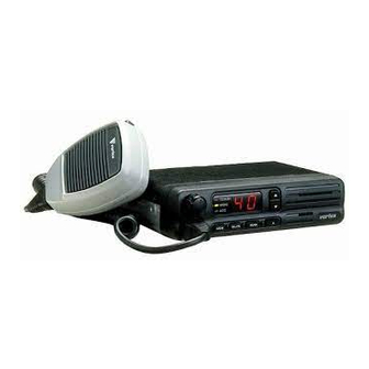
VHF Land Mobile Transceiver
VX-2000V
Service Manual
©2003 VERTEX STANDARD CO., LTD.
40 channel version
Introduction
This manual provides technical information necessary for servicing the VX-2000V VHF Land Mobile transceiver.
The VX-2000V is carefully designed to allow the knowledgeable operator to make nearly all adjustments required for
various station conditions, modes and operator preferences simply from the controls on the panels, without opening the
case of the transceiver. The VX-2000V Operating Manual describes these adjustments, plus certain internal settings.
Servicing this equipment requires expertise in handling surface mount chip components. Attempts by non-qualified
persons to service this equipment may result in permanent damage not covered by warranty.
For the major circuit boards, each side of the board is identified by the type of the majority of components installed on
that side.
In most cases one side has only chip components, and the other has either a mixture of both chip and lead components
(trimmers, coils, electrolytic capacitors, packaged ICs, etc.), or lead components only.
While we believe the technical information in this manual is correct, Vertex Standard assumes no liability for damage
that may occur as a result of typographical or other errors that may be present. Your cooperation in pointing out any
inconsistencies in the technical information would be appreciated. Vertex Standard reserves the right to make changes in
this transceiver and the alignment procedures, in the interest of technological improvement, without notification of the
owners.
Operating Manual Reprint ............................ 2
Specifications ................................................... 7
Exploded View & Miscellaneous Parts....... 8
Block Diagram ................................................. 9
Interconnection Diagram............................. 13
Circuit Description ...................................... 15
Alignment....................................................... 19
E095390A
4 channel version
Contents
Board Unit
Main Unit ............................................................... 23
Display-1 Unit ...................................................... 49
Display-2 Unit ...................................................... 53
Vr Unit ..................................................................... 57
Mic Unit .................................................................. 58
VERTEX STANDARD CO., LTD.
4-8-8 Nakameguro, Meguro-Ku, Tokyo 153-8644, Japan
VERTEX STANDARD
US Headquarters
10900 Walker Street, Cypress, CA 90630, U.S.A.
International Division
8350 N.W. 52nd Terrace, Suite 201, Miami, FL 33166, U.S.A.
YAESU EUROPE B.V.
P.O. Box 75525, 1118 ZN Schiphol, The Netherlands
YAESU UK LTD.
Unit 12, Sun Valley Business Park, Winnall Close
Winchester, Hampshire, SO23 0LB, U.K.
VERTEX STANDARD HK LTD.
Unit 5, 20/F., Seaview Centre, 139-141 Hoi Bun Road,
Kwun Tong, Kowloon, Hong Kong
(Schematics, Layouts & Parts)
1
Advertisement
Table of Contents

Related Manuals for Vertex Standard VX-2000V


Summary of Contents for Vertex Standard VX-2000V
-
Page 1: Operating Manual Reprint
This manual provides technical information necessary for servicing the VX-2000V VHF Land Mobile transceiver. The VX-2000V is carefully designed to allow the knowledgeable operator to make nearly all adjustments required for various station conditions, modes and operator preferences simply from the controls on the panels, without opening the case of the transceiver. -
Page 2: Operating Manual Reprint
Operating Manual Reprint & C ONTROLS ONNECTORS 4 channel version 40 channel version À The following items are unique to the 40-channel Microphone Jack Connect the microphone plug to this jack. radio versions: Æ CHANNEL Selector Buttons (p) and (q) Á... - Page 3 Operating Manual Reprint REAR (Heatsink) À 13.6V DC Cable Pigtail w/Connector The supplied DC power cable must be affixed to this 2-pin connector. Á Antenna Socket The 50-ohm coaxial feedline to the antenna must be con- nected here, using a “UHF” type (PL-259) plug. Â...
-
Page 4: Setting The Volume
Operating Manual Reprint PERATION Power O Scanning Turn the VOLUME/POWER knob clockwise to turn on the ra- To activate scanning on your radio, first place the microphone in dio. The active display and channel indicators will become illu- its hanger. Now press the SCAN button momentarily. The radio minated, indicating the status of the radio. -
Page 5: Ptional A Ccessories
Operating Manual Reprint ROGRAMMABLE HANNEL ELECTIONS nel, and hold in the SEL/PRI button for 2 seconds, until a beep You can program a list of channels to be scanned, and up to two channels to be monitored on a “priority” basis. Your selections sounds and the “P”... - Page 6 Operating Manual Reprint J1003 DSUB 9-Pin Data Connector Pin Assignment Ä Ã Â Á À È Ç Æ Å À SQ: Squelch Signal Output à Not Used Carrier In: Active High (5 V / 47 k ) Ä GND: Ground Á...
-
Page 7: Specifications
Specifications General Frequency Range (version): 134 ~160 or 148 ~ 174 MHz (VHF vers. A/C, respectively) No. of Channels & Spacing: 4 or 40 channels 25-kHz, 12.5-kHz spacing Modes of Emission: 16K0F3E ,11K0F3E Frequency Stability: ±0.00025% Antenna Requirements: 50 ohms, unbalanced (SO-239 socket) Voltage Requirements: 11.8 V to 15.6 V DC, negative ground Current Consumption (approx.): 250 mA Stby, 200 mA Rx, 6.5 A Tx... -
Page 8: Exploded View & Miscellaneous Parts
Exploded View & Miscellaneous Parts REF. VXSTD P/N Description Qty. U24208001 TAPTITE SCREW M2.6X8 (Lot. 1~5) À U20208001 BINDING HEAD SCREW M2.6X8 (Lot. 6~) Qty. VXSTD P/N Description Á U20306002 BINDING HEAD SCREW M3X6NI Q0000062 FUSE 10A Â U23205001 TAPTITE SCREW M2.6X5 T9021810 DC CABLE Ã... -
Page 9: Block Diagram
Block Diagram VX-2000V 4ch Front Panel Block Diagram VX-2000V 40ch Front Panel Block Diagram... - Page 10 Block Diagram Note:...
- Page 11 Block Diagram VX-2000V Main Unit Block Diagram...
- Page 12 Block Diagram Note:...
-
Page 13: Interconnection Diagram
Interconnection Diagram VX-2000V 4ch Front Interconnection Diagram... - Page 14 Interconnection Diagram VX-2000V 40ch Front Interconnection Diagram...
-
Page 15: Circuit Description
Circuit Description Receive Signal Path (CFWM450G) or CF1002 (CFWM450E) to strip away unwanted mixer products, and then is ap- Incoming RF energy from the antenna jack is plied to the limiter amplifier in Q1029, which re- delivered to the M Unit, and passes through moves any amplitude variations in the 450 kHz IF. -
Page 16: Transmit Inhibit
Circuit Description When a carrier appears at the discriminator, Automatic Transmitter Power Control noise is removed from the output, causing pin 33 RF output from the final amplifier is sampled of Q1039 to go "high," in turn causing the "B "... - Page 17 Circuit Description (2SB1201STP-FA), Q1040 (2SC4116GR), and quency of the VCO according to the phase dif- D1029 (02CZ5.6Y), with temperature compen- ference between the signals derived from the sation provided by thermistors TH1003/TH1004 VCO and the crystal reference oscillator. The and capacitors associated with the 17.25 MHz VCO is thus phase-locked to the crystal reference reference crystal, X1002.
- Page 18 Circuit Description Channel Selection & Display Channel Selection & Display (4-channel version) (40-channel version) The C button on the front panel causes The U and D buttons on the front panel HANNEL microprocessor Q1039 to select the operating fre- cause microprocessor Q1039 to select the oper- quency and CTCSS frequency data from serial ating frequency and CTCSS frequency data from EEPROM Q1049 (BR93LC66RF).
-
Page 19: Alignment
Alignment The VX-2000 is carefully aligned at the facto- of the malfunction has been clearly pinpointed and ry for the specified performance across the de- any/all faulty components replaced, and realign- signed frequency range. Realignment should, ment determined to be absolutely necessary. therefore, not be necessary except in the event of Required Test Equipment a component failure, or when altering the fre-... - Page 20 Alignment 50 W RF Signal Dummy Load Generator Alignment Preparation & Precautions Before beginning alignment, connect the trans- In-Line Wattmeter ceiver to the PC using the VPL-1 Connection Ca- ble, and upload the current frequency data from Deviation RF Sampling Transceiver meter Coupler...
- Page 21 Alignment Now select channel 1, and confirm that the nels 1 and 3, and confirm that 30 Watts of RF reading changes to about 1.0V for Version A, power is present on the band edge channels. or 0.8V for Version C. Using the computer, re-program channel 1 for Again select channel 3.
- Page 22 Alignment Restore Original Channel Data able DCS code 627 (encode), and download this data to the transceiver. When all alignment steps have been complet- With the AF generator still set to zero, key the ed, re-load the original channel data from your transmitter, and adjust VR1005 (MAIN Unit) computer’s disk, and download it to the trans- for ±900 Hz deviation on the DCS signal (with-...
-
Page 23: Main Unit
MAIN Unit (Lot. 1~) Circuit Diagram 13.5 (12.8) 13.8 (13.5) 0 (7.0) 3.4 (4.0) 0 (2.1) 7.1 (7.0) 7.5 (7.4) 13.5 (7.5) 0 (4.3) 2.8 2.9 (2.1) 0 (8.4) 0 (1.9) (4.0) 0 (5.1) 5.6 (5.5) 0 (6.7) (1.2) (5.0) 2.9 (4.3) 6.1 (0) 3.4 (0) - Page 24 MAIN Unit (Lot. 1~) Note:...
- Page 25 MAIN Unit (Lot. 1~) Parts Layout MB89P677ARFM (Lot. 1~) MX165BDW MB89677ARPFM (Lot. 2~) (Q1009) (Q1039) SC370651FR2 BA4116FV (Q1050) (Q1029) NJM2902V NJM2904V (Q1007, 1016) (Q1017) TDA2003H 2SB1143S (Q1003) (Q1014) Side A HA17805P 2SB1201STP (Q1010) (Q1002) 2SC4116GR (LG) (Q1015, 1042) (Q1048: Lot. 2~) 2SC4215Y (QY) (Q1026) MA143 (MC)
- Page 26 MAIN Unit (Lot. 1~) Side B 02CZ5.6Y (5.6) M67741H-01 BR93LC66RF IMH6 (H6) DTB123EK (F12) DTC124EU (25) 2SC4116GR (LG) HZM7C (24) (Lot. 2~) MA143 (MC) (D1018, 1029) (Q1011) (Q1049) (Q1004, 1025, 1052) (Q1006) (Q1020, 1033, 1051) (Q1040, 1045, 1047) (D1024) (D1040) (D1024: Lot.
- Page 27 MAIN Unit (Lot. 5~) Circuit Diagram...
- Page 28 MAIN Unit (Lot. 5~) Note:...
- Page 29 MAIN Unit (Lot. 5~) Parts Layout MB89P677ARFM (Lot. 1~) MX165BDW (Lot. 1~) MB89677ARPFM (Lot. 2~) MX165CDW (Lot. 6~) (Q1039) (Q1009) SC370651FR2 BA4116FV (Lot. 1~) (Q1050) TA31136FN (Lot. 7~) (Q1029) NJM2902V NJM2904V (Q1007, 1016) (Q1017) TDA2003H 2SB1143S (Q1003) (Q1014) Side A HA17805P 2SB1201STP (Q1010)
- Page 30 MAIN Unit (Lot. 5~) Side B 02CZ5.6Y (5.6) M67741H-01 BR93LC66RF IMH6 (H6) DTB123EK (F12) DTC124EU (25) 2SC4116GR (LG) HZM7C (24) (Lot. 2~) MA143 (MC) (D1018, 1029) M67741L-01 (Ver A: Lot. 6~) (Q1049) (Q1004, 1025, 1052) (Q1006) (Q1020, 1033, 1051) (Q1040, 1045, 1047) (D1024) (D1040) (D1024: Lot.
- Page 31 MAIN Unit (Lot. 19~) Circuit Diagram...
- Page 32 MAIN Unit (Lot. 19~) Note:...
- Page 33 MAIN Unit (Lot. 19~) Parts Layout MB89P677ARFM (Lot. 1~) MB89677ARPFM (Lot. 2~) MB89P677APFM (NTL: Lot. 53~) MB89677ARPFM (EXP, STANDARD, VTX: Lot. 53~) (Q1039) SC370651FR2 MX165BDW MX165CDW (Lot. 6~) MC145192FR2 (Lot. 26~) MC145193FR2 (Lot. 41~) (Q1009) (Q1050) BA4116FV TA31136FN (Lot. 7~) (Q1029) NJM2902V NJM2904V...
- Page 34 MAIN Unit (Lot. 19~) Side B 02CZ5.6Y (5.6) M67741H-01 BR93LC66RF IMH6 (H6) DTB123EK (F12) DTC124EU (25) 2SC4116GR (LG) HZM7C (24) (Lot. 2~62) HZM7.5NB (Lot. 63~) (D1018, 1029) (Q1011) BR93L66RF (Lot. 85~) (Q1004, 1025, 1052) (Q1006) (Q1020, 1033, 1051) (Q1040, 1045, 1047) (D1024) (D1024) (D1024: Lot.
-
Page 35: Main Unit
MAIN Unit Parts List REF. DESCRIPTION VALUE TOL. MFR’S DESIG VXSTD P/N VERS. LOT. SIDE. LAY ADR. *** MAIN UNIT *** PCB with Components CB0370001 TYPE C PCB with Components CB0370002 TYPE A Printed Circuit Board FR001570B Printed Circuit Board FR001570C Printed Circuit Board FR001570D... - Page 36 MAIN Unit REF. DESCRIPTION VALUE TOL. MFR’S DESIG VXSTD P/N VERS. LOT. SIDE. LAY ADR. C 1041 CHIP CAP. GRM39CH040C50PT K22174205 VERSION C 6- C 1042 CHIP CAP. 0.001uF GRM39B102M50PT K22174809 C 1044 CHIP CAP. 0.1uF GRM39B104K16PT K22124805 C 1045 CHIP CAP. 27pF GRM39CH270J50PT K22174221...
- Page 37 MAIN Unit REF. DESCRIPTION VALUE TOL. MFR’S DESIG VXSTD P/N VERS. LOT. SIDE. LAY ADR. C 1082 CHIP CAP. GRM42-6B105K16NPT K22121803 C 1083 AL.ELECTRO.CAP. 10uF ECEV1CS100SR K48120001 C 1084 CHIP CAP. 470pF GRM39CH471J50PT K22174249 C 1085 CHIP CAP. 0.001uF GRM39B102K50PT K22174821 C 1086 CHIP CAP.
- Page 38 MAIN Unit REF. DESCRIPTION VALUE TOL. MFR’S DESIG VXSTD P/N VERS. LOT. SIDE. LAY ADR. C 1123 CHIP CAP. 0.01uF GRM39B103M25PT K22144802 C 1124 CHIP CAP. 27pF GRM39CH270J50PT K22174221 C 1125 CHIP CAP. 0.047uF GRM39B473K16PT K22124804 C 1126 CHIP CAP. 560pF GRM39B561M50PT K22174806...
- Page 39 MAIN Unit REF. DESCRIPTION VALUE TOL. MFR’S DESIG VXSTD P/N VERS. LOT. SIDE. LAY ADR. C 1181 CHIP CAP. 100pF GRM39CH101J50PT K22174235 C 1182 CHIP CAP. 0.1uF GRM39B104K16PT K22124805 C 1183 CHIP CAP. 100pF GRM39CH101J50PT K22174235 C 1184 CHIP CAP. 100pF GRM39CH101J50PT K22174235...
- Page 40 MAIN Unit REF. DESCRIPTION VALUE TOL. MFR’S DESIG VXSTD P/N VERS. LOT. SIDE. LAY ADR. C 1234 CHIP CAP. 0.1uF GRM39B104K16PT K22124805 C 1235 CHIP CAP. 0.033uF GRM39R333K16PT K22124801 C 1236 CHIP CAP. 0.1uF GRM39B104K16PT K22124805 C 1237 CHIP TA.CAP. 10uF TEMSVA1A106M-8R K78100028...
- Page 41 MAIN Unit REF. DESCRIPTION VALUE TOL. MFR’S DESIG VXSTD P/N VERS. LOT. SIDE. LAY ADR. D 1016 DIODE DAP202U T106 G2070160 D 1017 DIODE MA143-(TX) G2070536 D 1018 DIODE 02CZ5.6Y TE85R G2070300 D 1019 DIODE MA142WK-(TX) G2070534 D 1021 DIODE 1SS355 TE-17 G2070470 D 1022 DIODE...
- Page 42 MAIN Unit LOT. REF. DESCRIPTION VALUE TOL. MFR’S DESIG VXSTD P/N VERS. SIDE. LAY ADR. L 1013 COIL E2 0.28-1.0-4.5T-R L0022395 L 1014 COIL E2 0.28-1.0-4.5T-R L0022395 L 1015 M.RFC 0.33uH LK1608 R33K-T L1690412 L 1015 M.RFC 0.39uH LK1608 R39K-T L1690413 VERSION A 6- L 1015 M.RFC...
- Page 43 R 1023 CHIP RES. 1/16W 5% RMC1/16 470JATP J24185470 R 1024 CHIP RES. 1/16W 5% RMC1/16 000JATP J24185000 R 1025 CHIP RES. 1/16W 5% RMC1/16 333JATP J24185333 R 1026 CHIP RES. 100k 1/16W 5% RMC1/16 104JATP J24185104 * Please contact VERTEX STANDARD.
- Page 44 MAIN Unit REF. DESCRIPTION VALUE TOL. MFR’S DESIG VXSTD P/N VERS. LOT. SIDE. LAY ADR. R 1027 CHIP RES. 1/16W 5% RMC1/16 153JATP J24185153 R 1028 CHIP RES. 1/16W 5% RMC1/16 123JATP J24185123 R 1029 CHIP RES. 6.8k 1/16W 5% RMC1/16 682JATP J24185682 R 1030 CHIP RES.
- Page 45 MAIN Unit REF. DESCRIPTION VALUE TOL. MFR’S DESIG VXSTD P/N VERS. LOT. SIDE. LAY ADR. R 1078 CHIP RES. 2.2M 1/16W 5% RMC1/16 225JATP J24185225 R 1079 CHIP RES. 1/16W 5% RMC1/16 331JATP J24185331 R 1080 CHIP RES. 100k 1/16W 5% RMC1/16 104JATP J24185104 R 1081 CHIP RES.
- Page 46 MAIN Unit REF. DESCRIPTION VALUE TOL. MFR’S DESIG VXSTD P/N VERS. LOT. SIDE. LAY ADR. R 1134 CHIP RES. 1/16W 5% RMC1/16 123JATP J24185123 R 1135 CHIP RES. 1.8M 1/16W 5% RMC1/16 185JATP J24185185 R 1135 CHIP RES. 3.3M 1/16W 5% RMC1/16 335JATP J24185335 R 1136 CHIP RES.
- Page 47 MAIN Unit REF. DESCRIPTION VALUE TOL. MFR’S DESIG VXSTD P/N VERS. LOT. SIDE. LAY ADR. R 1187 CHIP RES. 1/16W 5% RMC1/16 103JATP J24185103 R 1188 CHIP RES. 220k 1/16W 5% RMC1/16 224JATP J24185224 R 1188 CHIP RES. 1/16W 5% RMC1/16 683JATP J24185683 R 1189 CHIP RES.
- Page 48 MAIN Unit REF. DESCRIPTION VALUE TOL. MFR’S DESIG VXSTD P/N VERS. LOT. SIDE. LAY ADR. R 1240 CHIP RES. 1/16W 5% RMC1/16 223JATP J24185223 R 1241 CHIP RES. 270k 1/16W 5% RMC1/16 274JATP J24185274 R 1242 CHIP RES. 220k 1/16W 5% RMC1/16 224JATP J24185224 R 1243 CHIP RES.
-
Page 49: Display-1 Unit
Display-1 Unit Circuit Diagram... - Page 50 Display-1 Unit Parts Layout Side A Side B BU4094BCFV XN1213 (9L) DTC124EK (25) (Q2002) (Q2001, 2003, 2004) (Q2005)
-
Page 51: Parts List
Display-1 Unit Parts List REF. DESCRIPTION VALUE TOL. MFR’S DESIG VXSTD P/N VERS. LOT. SIDE. LAY ADR. *** DISPLAY-1 UNIT *** PCB with Components CB0382001 Printed Circuit Board FR001580B D 2001 LED HLMP-1540 G2090696 D 2002 LED HLMP-1540 G2090696 D 2003 LED HLMP-1540 G2090696 D 2004 LED... - Page 52 Display-1 Unit Note:...
-
Page 53: Display-2 Unit
Display-2 Unit Circuit Diagram... - Page 54 Display-2 Unit Parts Layout Side A Side B DN8657S DTC124EK (25) (Q3001) (Q3003) Dig.1 Dig.2 D.P2 D.P1 A1 B1 C1 D1 E1 F1 G1 A2 B2 C2 D2 E2 F2 G2 16 15 1 18 17 11 10 XN1213 (9L) (Q3002) DS3001 7-Segment LCD Display...
- Page 55 Display-2 Unit Parts List REF. DESCRIPTION VALUE TOL. MFR’S DESIG VXSTD P/N VERS. LOT. SIDE. LAY ADR. *** DISPLAY-2 UNIT *** PCB with Components CB0383001 Printed Circuit Board FR001590B D 3002 DIODE 1SS355 TE-17 G2070470 D 3003 LED TLY211 G2090637 D 3004 DIODE 1SS355 TE-17 G2070470...
- Page 56 Display-2 Unit Note:...
- Page 57 VR Unit Circuit Diagram Parts Layout Side A Side B Parts List REF. DESCRIPTION VALUE TOL. MFR’S DESIG VXSTD P/N VERS. LOT. SIDE. LAY ADR. *** VR UNIT *** PCB with Components CB0384001 Printed Circuit Board FR001600B VR4001 POT. RK0971111 10KB/SW J60800228...
-
Page 58: Mic Unit
MIC Unit Circuit Diagram Parts Layout Side A Side B Parts List REF. DESCRIPTION VALUE TOL. MFR’S DESIG VXSTD P/N VERS. LOT. SIDE. LAY ADR. *** MIC UNIT *** PCB with Components CB0384001 Printed Circuit Board FR001600B J 5001 CONNECTOR R41-2509H P1090714 JP5001 WIRE ASSY... - Page 59 No portion of this manual © Copyright 2003 may be reproduced VERTEX STANDARD CO., LTD. without the ermission of All rights reserved VERTEX STANDARD CO., LTD.
Need help?
Do you have a question about the VX-2000V and is the answer not in the manual?
Questions and answers